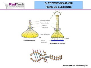
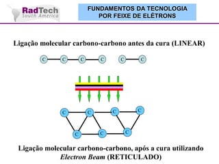
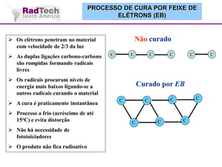
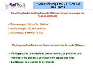
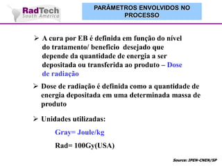
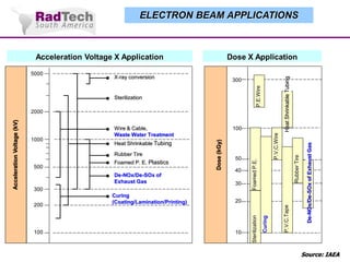
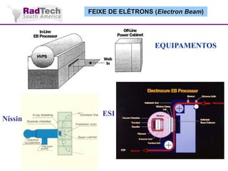
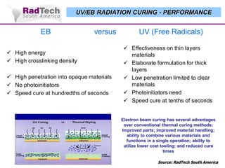
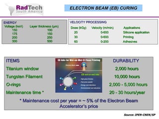
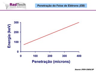
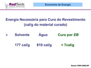
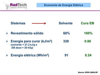
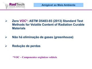
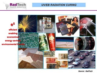
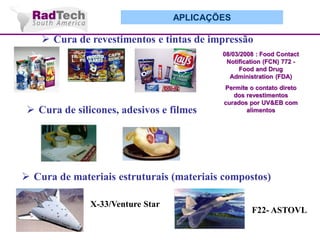
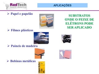
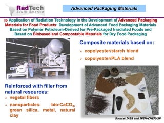
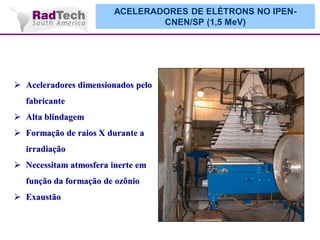
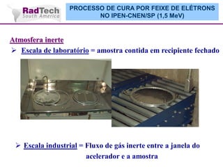
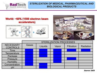
FEIXE DE ELÉTRONS NA
CURA POR RADIAÇÃO E
SUAS APLICAÇÕES
Wilson Aparecido Parejo Calvo
Centro de Tecnologia das Radiações
IPEN-CNEN/SP
wapcalvo@ipen.br

Paulo Roberto Rela

CBE
prela06@yahoo.com.br
APPLICATIONS OF RADIATION AND
RADIOISOTOPES TECHNIQUES IN INDUSTRY
Residence Time Distribution
Mass balance
Thin Layer Activation
Gamma scanning
Neutron backscattering
Computer Fluid Dynamics
Single Particle Tracking
Emission computer tomography
Radiography
Digital radioscopy
Computer tomography
Nuclear related techniques

RADIOTRACERS AND
SEALED SOURCES

NDT

INDUSTRY

Gamma irradiation
Electron beam irradiation
Accelerator irradiation
Ion beam irradiation

RADIATION
PROCESSING

NUCLEONICS
GAUGES

NUCLEAR
ANALYTICAL
TECHNIQUES

Transmission
Backscattering
Multibeam & multienergy
Computer tomography
Low activity
Prompt Gamma (PGNAA)
Delayed gamma (DGNAA)
Gamma loggers

X-ray fluorescence (XRF)
Neutron activation analysis (NAA)
Ion beam analysis
Radiometric measurements
Related techniques

Source: IAEA
Gamma Rays, Electron Beam and X-Rays

Gamma Rays (60Co)

X-Rays

(10 MeV, 50 kW)
50 cm (1,0 g/cm3)
10 kGy/h

Electron Beam

(5–7 MeV)

5 cm (1,0 g/cm3)
72 MGy/h

> 50 cm (1,0 g/cm3)
100 kGy/h

Source: IBA and IPEN-CNEN/SP
SISTEMAS DE CURA (Térmica, UV e EB)

DILUENTE REATIVO

ADITIVOS

ADITIVOS

RESINA

RESINA

PIGMENTOS

SISTEMA
CONVENCIONAL

PIGMENTOS

DILUENTE REATIVO
FOTOINICIADOR

SOLVENTE

SISTEMA UV

ADITIVOS
RESINA
PIGMENTOS

SISTEMA EB

Source: RadTech South America
ELECTRON BEAM (EB)
FEIXE DE ELÉTRONS

Source: IBA and IPEN-CNEN/SP
FUNDAMENTOS DA TECNOLOGIA
POR FEIXE DE ELÉTRONS

Ligação molecular carbono-carbono antes da cura (LINEAR)
C

C

C

C

C

C

C

C

C

C

C

C

C

Ligação molecular carbono-carbono, após a cura utilizando
Electron Beam (RETICULADO)
PROCESSO DE CURA POR FEIXE DE
ELÉTRONS (EB)

Não curado

 Os elétrons penetram no material
com velocidade de 2/3 da luz
 As duplas ligações carbono-carbono
são rompidas formando radicais
livres

C

C

 Os radicais procuram níveis de
energia mais baixos ligando-se a
outros radicais curando o material
 A cura é praticamente instantânea
 Processo a frio (acréscimo de até
15oC) e evita distorção

 Não há necessidade de
fotoiniciadores
 O produto não fica radioativo

C

C

C

C

Curado por EB
C

C

C

C

C

C

C
ACELERADORES INDUSTRIAIS DE
ELÉTRONS
Classificação dos Aceleradores de Elétrons (função da energia do
feixe de elétrons)

 Baixa energia: 150 keV to 300 keV
 Média energia: 300 keV to 5 MeV
 Alta energia: 5 MeV to 10 MeV

Vantagens e Limitações no Processamento por Feixe de Elétrons
 Vantagens: alta velocidade de processamento de produtos bem
definidos e de grandes superfícies com espessuras finas
 Limitações: baixo poder de penetração
PARÂMETROS ENVOLVIDOS NO
PROCESSO

 A cura por EB é definida em função do nível
do tratamento/ beneficio desejado que
depende da quantidade de energia a ser
depositada ou transferida ao produto – Dose
de radiação
 Dose de radiação é definida como a quantidade de
energia depositada em uma determinada massa de
produto
 Unidades utilizadas:

Gray= Joule/kg
Rad= 100Gy(USA)
Source: IPEN-CNEN/SP
ELECTRON BEAM APPLICATIONS

300

500

Foamed P. E. Plastics
De-NOx/De-SOx of
Exhaust Gas

40

30

300
200

100

Curing
(Coating/Lamination/Printing)

P.V.C.Wire

50

20

10

Curing

Rubber Tire

Foamed P.E.

Heat Shrinkable Tubing

100

Sterilization

1000

Wire & Cable,
Waste Water Treatment

Dose (kGy)

Acceleration Voltage (kV)

2000

Rubber Tire

Sterilization

De-NOx/De-SOx of Exhaust Gas

Heat Shrinkable Tubing

X-ray conversion

P.E.Wire

5000

Dose X Application

P.V.C.Tape

Acceleration Voltage X Application

Source: IAEA
Agência Internacional de Energia
Atômica (IAEA)
IAEA Specific Safety Guide
SSG-8
Radiation Safety of Gamma,
Electron and X Ray
Irradiation Facilities

Categoria I
Categoria II
FEIXE DE ELÉTRONS (Electron Beam)

EQUIPAMENTOS

Nissin

ESI
UV/EB RADIATION CURING - Equipments

Energy Scineces, Inc. (ESI)
(www.ebeam.com)
Web widths: 20 to 66” (508 to 1,676 mm)
Speed capability: 335 m/min
Thickness: 0.03 mm

Web widths: 30 to 120” (762 to 3,048
mm)
Speed capability: 305 m/min

Thickness: 0.35 mm
Source: ESI
UV/EB RADIATION CURING - Equipments

PCT Engineered Systems, LLC
(www.teampct.com)

Voltage: 70 to 125 keV

Voltage: 125 to 300 keV

Web widths: 36”(914mm) to 68”(1,727mm)

Web widths: 130” (3,300 mm)
Source: PCT
AEB two module pilot line
AEB two modules production line
Descontaminação superficial (EB)

AEB unit for surface decontamination
41 cm x 6.3 cm beam window
21 cm diameter module
EB Compacto
Unidade de Laboratório

Acelerador de
elétrons

Blindagem do
sistema de
transporte

Painel de
controle

Fonte de
alimentação

CLP/computador
UV/EB RADIATION CURING - PERFORMANCE

EB

versus

 High energy
 High crosslinking density

 High penetration into opaque materials
 No photoinitiators
 Speed cure at hundredths of seconds

UV (Free Radicals)
 Effectiveness on thin layers
materials
 Elaborate formulation for thick
layers
 Low penetration limited to clear
materials
 Photoinitiators need
 Speed cure at tenths of seconds

Electron beam curing has several advantages
over conventional thermal curing methods:
Improved parts; improved material handling;
ability to combine various materials and
functions in a single operation; ability to
utilize lower cost tooling; and reduced cure
times
Source: RadTech South America
ELECTRON BEAM (EB) CURING
ENERGY
Voltage (keV)
150
175
200
300

VELOCITY PROCESSING
Layer thickness (µm)
100
150
250
500

ITEMS

Dose (kGy)
20

Velocity (m/min)
0-600

Applications
Silicone application

30

0-600

Printing

60

0-200

Adhesives

DURABILITY

Titanium window

2,000 hours

Tungsten Filament

10,000 hours

O-rings

2,000 - 5,000 hours

Maintenance time *

20 - 30 hours/year

* Maintenance cost per year = ~ 5% of the Electron Beam
Accelerator’s price
Source: IPEN-CNEN/SP
Penetração do Feixe de Elétrons (EB)

Energia (keV)

300

200

100

0

0

100

200

300

400

Penetração (microns)
Source: IPEN-CNEN/SP
Economia de Energia

Energia Necessária para Cura do Revestimento
(cal/g do material curado)


Solvente
177 cal/g

Água
810 cal/g

Cura por EB
< 7cal/g

Source: IPEN-CNEN/SP
Economia de Energia Elétrica

Sistemas

Solvente

Cura EB

 Revestimento sólido

60%

100%

 Energia para curar (kJ/m2)

328

0.86

91

0.24

(solvente = 27,3 kJ/g e
EB dose = 30 kGy)

 Energia elétrica (Wh/m2)

Source: IPEN-CNEN/SP
Amigável ao Meio Ambiente



Zero VOC*: ASTM D5403-93 (2013) Standard Test
Methods for Volatile Content of Radiation Curable
Materials



Não há eliminação de gases (greenhouse)



Redução de perdas

*VOC – Componentes orgânicos voláteis
Amigável ao Meio Ambiente

Sistemas
 Sólidos no revestimento
 Revestimento seco (g/m2)
 VOC*/m2, g

Solvente
60%
20 g
12 g

Cura EB
100%
20 g
0g

(Solvente = 0,9 g/cm3)

 CO2 do solvente
(Incineração do solvente)
*VOC – Componentes orgânicos voláteis

7 g/m2

não há
Custo Anual de Processamento

Source: Radtech (USA) 2006
COMPARAÇÃO DOS CUSTOS NA IMPRESSÃO DE
EMBALAGEM PARA PRODUTO ALIMENTÍCIO
MERCADO PARA OS ACELERADORES DE
ELÉTRONS (150keV – 300keV)

América do Norte (RadTec 2006): mercado de 5 a 10% das
curas por radiação (UV/EB)
Mercado total de produtos UV/EB (2005) = 95.000 ton
Gary Cohen Executive Director RadTech 2006
Aplicações dos Aceleradores
Industriais de Elétrons
150 keV - 300 keV
UV/EB RADIATION CURING

e5
efficient

enabling
economical

energy savings
environmental friendly

Source: RadTech
APLICAÇÕES

 Cura de revestimentos e tintas de impressão
08/03/2008 : Food Contact
Notification (FCN) 772 Food and Drug
Administration (FDA)

 Cura de silicones, adesivos e filmes

Permite o contato direto
dos revestimentos
curados por UV&EB com
alimentos

 Cura de materiais estruturais (materiais compostos)
X-33/Venture Star

F22- ASTOVL
APLICAÇÕES

 Papel e papelão

 Filmes plásticos

 Paineis de madeira

 Bobinas metálicas

SUBSTRATOS
ONDE O FEIXE DE
ELÉTRONS PODE
SER APLICADO
Advanced Packaging Materials
 Application of Radiation Technology in the Development of Advanced Packaging
Materials for Food Products: Development of Advanced Food Packaging Materials
Based on Polymer Petroleum-Derived for Pre-Packaged Irradiated Foods and
Based on Biobased and Compostable Materials for Dry Food Packaging

Source: IAEA and IPEN-CNEN/SP
Aplicações dos Aceleradores
Industriais de Elétrons
300 keV - 10 MeV
ACELERADORES DE ELÉTRONS NO IPENCNEN/SP (1,5 MeV)

 Aceleradores dimensionados pelo
fabricante
 Alta blindagem

 Formação de raios X durante a
irradiação
 Necessitam atmosfera inerte em

função da formação de ozônio
 Exaustão
PROCESSO DE CURA POR FEIXE DE ELÉTRONS
NO IPEN-CNEN/SP (1,5 MeV)

Atmosfera inerte
 Escala de laboratório = amostra contida em recipiente fechado

 Escala industrial = Fluxo de gás inerte entre a janela do
acelerador e a amostra
IRRADIATION OF WIRE/ELECTRIC CABLES AND
POLYETHILINE FOAM

ACOME (Brazil) = 15,000 km/month
Source: IPEN-CNEN/SP
HEAT SHRINKABLE TUBES IRRADIATION

SEMICONDUCTORS IRRADIATION and POLYMER DEGRADATION

Powered
Diodes

PTFE (TeflonTM)
Source: IAEA and IPEN-CNEN/SP
IRRADIATION OF TIRES COMPONENTES

Japan: Automobiles

tires = 95%

BRAZIL: Bridgestone-Firestone
Source: IPEN-CNEN/SP
Materiais Compósitos

 Indústrias Automobilísticas e
Aeroespaciais
Materiais Compósitos
ACELETRON INDUSTRIAL IRRADIATION

18 kW (10 MeV)

Source: ACELETRON
FOOD IRRADIATION
• Military Food (10-50kGy)
• Potatoes and Onions (0.05-0.15kGy)

• Bread (2-10kGy)
• Strawberries (0.2-1.0kGy)

Brazilian Agrobusiness:
43% of the total exportation

Source: IPEN-CNEN/SP
RHODOTRON
TT200 (100 kW)
 Radiation Curing of
Composites for Enhancing
their Features and Utility in
Health Care and Industry:
Development of Radiation
Processing to Functionalize
Carbon Nanofiber to Use in
Nanocomposite for
Industrial Application

Sterilized
Medical
Devices:
135.000
m³/year

Source: IAEA, IPEN-CNEN/SP and CBE
STERILIZATION OF MEDICAL, PHARMACEUTICAL AND
BIOLOGICAL PRODUCTS

World: ~60% (1500 electron beam
accelerators)

STERILIZATION PROCESSES
NECESSARY
CONTROLS
Time
Temperature
Package
Pressure
Humidity
Concentration
pH

Gases
xxxxxx
xxxxxx
xxxxxx
xxxxxx
xxxxxx
xxxxxx

Liquids

Vapor

Filtration

Radiation

xxxxxx
xxxxxx
xxxxxx

xxxxxx
xxxxxx
xxxxxx
xxxxxx
xxxxxx

xxxxxxx

xxxxxxx

xxxxxxx

xxxxxx
xxxxxx
Source: IAEA
MOBILE ELECTRON ACCELERATOR

Beam Energy: 0.4 ~ 0.7
MeV
Beam Power: 20 kW
Total weight: 40 tons

Source: EB-Tech
Mobile e-beam in flue gas purification from oilrefinery in Saudi Arabia

Source: EB-Tech
MUITO
OBRIGADO !

CURSO BÁSICO RADTECH - FEIXE DE ELÉTRONS

  • 1.
    FEIXE DE ELÉTRONSNA CURA POR RADIAÇÃO E SUAS APLICAÇÕES Wilson Aparecido Parejo Calvo Centro de Tecnologia das Radiações IPEN-CNEN/SP wapcalvo@ipen.br Paulo Roberto Rela CBE prela06@yahoo.com.br
  • 2.
    APPLICATIONS OF RADIATIONAND RADIOISOTOPES TECHNIQUES IN INDUSTRY Residence Time Distribution Mass balance Thin Layer Activation Gamma scanning Neutron backscattering Computer Fluid Dynamics Single Particle Tracking Emission computer tomography Radiography Digital radioscopy Computer tomography Nuclear related techniques RADIOTRACERS AND SEALED SOURCES NDT INDUSTRY Gamma irradiation Electron beam irradiation Accelerator irradiation Ion beam irradiation RADIATION PROCESSING NUCLEONICS GAUGES NUCLEAR ANALYTICAL TECHNIQUES Transmission Backscattering Multibeam & multienergy Computer tomography Low activity Prompt Gamma (PGNAA) Delayed gamma (DGNAA) Gamma loggers X-ray fluorescence (XRF) Neutron activation analysis (NAA) Ion beam analysis Radiometric measurements Related techniques Source: IAEA
  • 3.
    Gamma Rays, ElectronBeam and X-Rays Gamma Rays (60Co) X-Rays (10 MeV, 50 kW) 50 cm (1,0 g/cm3) 10 kGy/h Electron Beam (5–7 MeV) 5 cm (1,0 g/cm3) 72 MGy/h > 50 cm (1,0 g/cm3) 100 kGy/h Source: IBA and IPEN-CNEN/SP
  • 4.
    SISTEMAS DE CURA(Térmica, UV e EB) DILUENTE REATIVO ADITIVOS ADITIVOS RESINA RESINA PIGMENTOS SISTEMA CONVENCIONAL PIGMENTOS DILUENTE REATIVO FOTOINICIADOR SOLVENTE SISTEMA UV ADITIVOS RESINA PIGMENTOS SISTEMA EB Source: RadTech South America
  • 5.
    ELECTRON BEAM (EB) FEIXEDE ELÉTRONS Source: IBA and IPEN-CNEN/SP
  • 6.
    FUNDAMENTOS DA TECNOLOGIA PORFEIXE DE ELÉTRONS Ligação molecular carbono-carbono antes da cura (LINEAR) C C C C C C C C C C C C C Ligação molecular carbono-carbono, após a cura utilizando Electron Beam (RETICULADO)
  • 7.
    PROCESSO DE CURAPOR FEIXE DE ELÉTRONS (EB) Não curado  Os elétrons penetram no material com velocidade de 2/3 da luz  As duplas ligações carbono-carbono são rompidas formando radicais livres C C  Os radicais procuram níveis de energia mais baixos ligando-se a outros radicais curando o material  A cura é praticamente instantânea  Processo a frio (acréscimo de até 15oC) e evita distorção  Não há necessidade de fotoiniciadores  O produto não fica radioativo C C C C Curado por EB C C C C C C C
  • 8.
    ACELERADORES INDUSTRIAIS DE ELÉTRONS Classificaçãodos Aceleradores de Elétrons (função da energia do feixe de elétrons)  Baixa energia: 150 keV to 300 keV  Média energia: 300 keV to 5 MeV  Alta energia: 5 MeV to 10 MeV Vantagens e Limitações no Processamento por Feixe de Elétrons  Vantagens: alta velocidade de processamento de produtos bem definidos e de grandes superfícies com espessuras finas  Limitações: baixo poder de penetração
  • 9.
    PARÂMETROS ENVOLVIDOS NO PROCESSO A cura por EB é definida em função do nível do tratamento/ beneficio desejado que depende da quantidade de energia a ser depositada ou transferida ao produto – Dose de radiação  Dose de radiação é definida como a quantidade de energia depositada em uma determinada massa de produto  Unidades utilizadas: Gray= Joule/kg Rad= 100Gy(USA) Source: IPEN-CNEN/SP
  • 10.
    ELECTRON BEAM APPLICATIONS 300 500 FoamedP. E. Plastics De-NOx/De-SOx of Exhaust Gas 40 30 300 200 100 Curing (Coating/Lamination/Printing) P.V.C.Wire 50 20 10 Curing Rubber Tire Foamed P.E. Heat Shrinkable Tubing 100 Sterilization 1000 Wire & Cable, Waste Water Treatment Dose (kGy) Acceleration Voltage (kV) 2000 Rubber Tire Sterilization De-NOx/De-SOx of Exhaust Gas Heat Shrinkable Tubing X-ray conversion P.E.Wire 5000 Dose X Application P.V.C.Tape Acceleration Voltage X Application Source: IAEA
  • 11.
    Agência Internacional deEnergia Atômica (IAEA) IAEA Specific Safety Guide SSG-8 Radiation Safety of Gamma, Electron and X Ray Irradiation Facilities Categoria I Categoria II
  • 12.
    FEIXE DE ELÉTRONS(Electron Beam) EQUIPAMENTOS Nissin ESI
  • 13.
    UV/EB RADIATION CURING- Equipments Energy Scineces, Inc. (ESI) (www.ebeam.com) Web widths: 20 to 66” (508 to 1,676 mm) Speed capability: 335 m/min Thickness: 0.03 mm Web widths: 30 to 120” (762 to 3,048 mm) Speed capability: 305 m/min Thickness: 0.35 mm Source: ESI
  • 14.
    UV/EB RADIATION CURING- Equipments PCT Engineered Systems, LLC (www.teampct.com) Voltage: 70 to 125 keV Voltage: 125 to 300 keV Web widths: 36”(914mm) to 68”(1,727mm) Web widths: 130” (3,300 mm) Source: PCT
  • 15.
    AEB two modulepilot line
  • 16.
    AEB two modulesproduction line
  • 17.
    Descontaminação superficial (EB) AEBunit for surface decontamination 41 cm x 6.3 cm beam window 21 cm diameter module
  • 18.
    EB Compacto Unidade deLaboratório Acelerador de elétrons Blindagem do sistema de transporte Painel de controle Fonte de alimentação CLP/computador
  • 19.
    UV/EB RADIATION CURING- PERFORMANCE EB versus  High energy  High crosslinking density  High penetration into opaque materials  No photoinitiators  Speed cure at hundredths of seconds UV (Free Radicals)  Effectiveness on thin layers materials  Elaborate formulation for thick layers  Low penetration limited to clear materials  Photoinitiators need  Speed cure at tenths of seconds Electron beam curing has several advantages over conventional thermal curing methods: Improved parts; improved material handling; ability to combine various materials and functions in a single operation; ability to utilize lower cost tooling; and reduced cure times Source: RadTech South America
  • 20.
    ELECTRON BEAM (EB)CURING ENERGY Voltage (keV) 150 175 200 300 VELOCITY PROCESSING Layer thickness (µm) 100 150 250 500 ITEMS Dose (kGy) 20 Velocity (m/min) 0-600 Applications Silicone application 30 0-600 Printing 60 0-200 Adhesives DURABILITY Titanium window 2,000 hours Tungsten Filament 10,000 hours O-rings 2,000 - 5,000 hours Maintenance time * 20 - 30 hours/year * Maintenance cost per year = ~ 5% of the Electron Beam Accelerator’s price Source: IPEN-CNEN/SP
  • 21.
    Penetração do Feixede Elétrons (EB) Energia (keV) 300 200 100 0 0 100 200 300 400 Penetração (microns) Source: IPEN-CNEN/SP
  • 22.
    Economia de Energia EnergiaNecessária para Cura do Revestimento (cal/g do material curado)  Solvente 177 cal/g Água 810 cal/g Cura por EB < 7cal/g Source: IPEN-CNEN/SP
  • 23.
    Economia de EnergiaElétrica Sistemas Solvente Cura EB  Revestimento sólido 60% 100%  Energia para curar (kJ/m2) 328 0.86 91 0.24 (solvente = 27,3 kJ/g e EB dose = 30 kGy)  Energia elétrica (Wh/m2) Source: IPEN-CNEN/SP
  • 24.
    Amigável ao MeioAmbiente  Zero VOC*: ASTM D5403-93 (2013) Standard Test Methods for Volatile Content of Radiation Curable Materials  Não há eliminação de gases (greenhouse)  Redução de perdas *VOC – Componentes orgânicos voláteis
  • 25.
    Amigável ao MeioAmbiente Sistemas  Sólidos no revestimento  Revestimento seco (g/m2)  VOC*/m2, g Solvente 60% 20 g 12 g Cura EB 100% 20 g 0g (Solvente = 0,9 g/cm3)  CO2 do solvente (Incineração do solvente) *VOC – Componentes orgânicos voláteis 7 g/m2 não há
  • 26.
    Custo Anual deProcessamento Source: Radtech (USA) 2006
  • 27.
    COMPARAÇÃO DOS CUSTOSNA IMPRESSÃO DE EMBALAGEM PARA PRODUTO ALIMENTÍCIO
  • 28.
    MERCADO PARA OSACELERADORES DE ELÉTRONS (150keV – 300keV) América do Norte (RadTec 2006): mercado de 5 a 10% das curas por radiação (UV/EB) Mercado total de produtos UV/EB (2005) = 95.000 ton Gary Cohen Executive Director RadTech 2006
  • 29.
    Aplicações dos Aceleradores Industriaisde Elétrons 150 keV - 300 keV
  • 30.
    UV/EB RADIATION CURING e5 efficient enabling economical energysavings environmental friendly Source: RadTech
  • 31.
    APLICAÇÕES  Cura derevestimentos e tintas de impressão 08/03/2008 : Food Contact Notification (FCN) 772 Food and Drug Administration (FDA)  Cura de silicones, adesivos e filmes Permite o contato direto dos revestimentos curados por UV&EB com alimentos  Cura de materiais estruturais (materiais compostos) X-33/Venture Star F22- ASTOVL
  • 32.
    APLICAÇÕES  Papel epapelão  Filmes plásticos  Paineis de madeira  Bobinas metálicas SUBSTRATOS ONDE O FEIXE DE ELÉTRONS PODE SER APLICADO
  • 33.
    Advanced Packaging Materials Application of Radiation Technology in the Development of Advanced Packaging Materials for Food Products: Development of Advanced Food Packaging Materials Based on Polymer Petroleum-Derived for Pre-Packaged Irradiated Foods and Based on Biobased and Compostable Materials for Dry Food Packaging Source: IAEA and IPEN-CNEN/SP
  • 34.
    Aplicações dos Aceleradores Industriaisde Elétrons 300 keV - 10 MeV
  • 35.
    ACELERADORES DE ELÉTRONSNO IPENCNEN/SP (1,5 MeV)  Aceleradores dimensionados pelo fabricante  Alta blindagem  Formação de raios X durante a irradiação  Necessitam atmosfera inerte em função da formação de ozônio  Exaustão
  • 36.
    PROCESSO DE CURAPOR FEIXE DE ELÉTRONS NO IPEN-CNEN/SP (1,5 MeV) Atmosfera inerte  Escala de laboratório = amostra contida em recipiente fechado  Escala industrial = Fluxo de gás inerte entre a janela do acelerador e a amostra
  • 37.
    IRRADIATION OF WIRE/ELECTRICCABLES AND POLYETHILINE FOAM ACOME (Brazil) = 15,000 km/month Source: IPEN-CNEN/SP
  • 38.
    HEAT SHRINKABLE TUBESIRRADIATION SEMICONDUCTORS IRRADIATION and POLYMER DEGRADATION Powered Diodes PTFE (TeflonTM) Source: IAEA and IPEN-CNEN/SP
  • 39.
    IRRADIATION OF TIRESCOMPONENTES Japan: Automobiles tires = 95% BRAZIL: Bridgestone-Firestone Source: IPEN-CNEN/SP
  • 40.
    Materiais Compósitos  IndústriasAutomobilísticas e Aeroespaciais
  • 41.
  • 42.
    ACELETRON INDUSTRIAL IRRADIATION 18kW (10 MeV) Source: ACELETRON
  • 43.
    FOOD IRRADIATION • MilitaryFood (10-50kGy) • Potatoes and Onions (0.05-0.15kGy) • Bread (2-10kGy) • Strawberries (0.2-1.0kGy) Brazilian Agrobusiness: 43% of the total exportation Source: IPEN-CNEN/SP
  • 44.
    RHODOTRON TT200 (100 kW) Radiation Curing of Composites for Enhancing their Features and Utility in Health Care and Industry: Development of Radiation Processing to Functionalize Carbon Nanofiber to Use in Nanocomposite for Industrial Application Sterilized Medical Devices: 135.000 m³/year Source: IAEA, IPEN-CNEN/SP and CBE
  • 45.
    STERILIZATION OF MEDICAL,PHARMACEUTICAL AND BIOLOGICAL PRODUCTS World: ~60% (1500 electron beam accelerators) STERILIZATION PROCESSES NECESSARY CONTROLS Time Temperature Package Pressure Humidity Concentration pH Gases xxxxxx xxxxxx xxxxxx xxxxxx xxxxxx xxxxxx Liquids Vapor Filtration Radiation xxxxxx xxxxxx xxxxxx xxxxxx xxxxxx xxxxxx xxxxxx xxxxxx xxxxxxx xxxxxxx xxxxxxx xxxxxx xxxxxx Source: IAEA
  • 46.
    MOBILE ELECTRON ACCELERATOR BeamEnergy: 0.4 ~ 0.7 MeV Beam Power: 20 kW Total weight: 40 tons Source: EB-Tech
  • 47.
    Mobile e-beam influe gas purification from oilrefinery in Saudi Arabia Source: EB-Tech
  • 48.