
Recomendados
Recomendados
Mais conteúdo relacionado
Mais procurados
Mais procurados (20)
Semelhante a Original IGBT 6MBP20XSF060-50 20XSF060 060 20A 600V New Fuji
Semelhante a Original IGBT 6MBP20XSF060-50 20XSF060 060 20A 600V New Fuji (20)
Mais de AUTHELECTRONIC
Mais de AUTHELECTRONIC (20)
Último
Último (20)
Original IGBT 6MBP20XSF060-50 20XSF060 060 20A 600V New Fuji
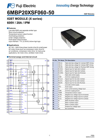
- 1. 1 6MBP20XSF060-50 IGBT Modules IGBT MODULE (X series) 600V / 20A / IPM Features Low-side IGBTs are separate emitter type Short circuit protection Temperature sensor output function Overheating protection Under voltage protection Fault signal output function Input interface : TTL (3.3V/5V) Active high logic Applications AC 100 ~ 240V three phase inverter drive for small power AC motor drives (such as compressor motor drive for air conditioner, compressor motor drive for heat pump applications, fan motor drive, ventilator motor drive) Terminal assign and Internal circuit Pin No. Pin Name Pin Description 3 VB (U) High-side bias voltage for U-phase IGBT driving 5 VB (V) High-side bias voltage for V-phase IGBT driving 7 VB (W) High-side bias voltage for W-phase IGBT driving 9 IN (HU) Signal input for high side U-phase 10 IN (HV) Signal input for high side V-phase 11 IN (HW) Signal input for high side W-phase 12 VCCH High-side control supply 13 COM Common supply ground 14 IN (LU) Signal input for low side U-phase 15 IN (LV) Signal input for low side V-phase 16 IN(LW) Signal input for low side W-phase 17 VCCL Low-side control supply 18 VFO Fault output 19 IS Over current sensing voltage input 20 COM Common supply ground 21 TEMP Temperature sensor output 22 N (W) Negative bus voltage input for W-phase 23 N (V) Negative bus voltage input for V-phase 24 N (U) Negative bus voltage input for U-phase 26 W Motor W-phase output 28 V Motor V-phase output 30 U Motor U-phase output 32 P Positive bus voltage input 36 NC No Connection 1696b MARCH 2016 VB(U) 11 10 9 5 3 21 20 19 18 17 16 15 14 13 12 22 23 24 26 28 30 36 32 U P V W N(V) N(U) N(W) Vcc IN GND OUT Vs Vcc UIN VIN WIN UOUT VOUT WOUT Fo IS GND VFO IS COM COM IN(LU) IN(LV) IN(LW) VCCL VCCH IN(HU) IN(HV) IN(HW) VB(V) VB(W) TEMP NC VB 7 TEMP Vcc IN GND OUT Vs VB Vcc IN GND OUT Vs VB
- 2. 2 6MBP20XSF060-50 IGBT Modules 1696b MARCH 2016 Absolute Maximum Ratings at Tj=25°C, VCC=15V (unless otherwise specified) Items Symbol Characteristics Unit Remarks Inverterblock DC Bus Voltage VDC 450 V Note *1 Bus Voltage (Surge) VDC(Surge) 500 V Note *1 Collector-Emitter Voltage VCES 600 V Collector Current IC@25 20 A Note *2 Peak Collector Current ICP@25 40 A VCC≧15V, VB(*)≧15V Note *2, *3, *4 30 A VCC≧13V, VB(*)≧13V Note *2, *3, *4 Diode Forward current IF@25 20 A Note *2 Peak Diode Forward current IFP@25 40 A Note *2 Collector Power Dissipation PD_IGBT 41.0 W per single IGBT TC=25°C FWD Power Dissipation PD_FWD 27.8 W per single FWD TC=25°C Junction Temperature Tj 150 °C Operating Junction Temperature TjOP -40 ~ +150 °C Controlcircuitblock High-side Supply Voltage VCCH -0.5 ~ 20 V Applied between VCCH-COM Low-side Supply Voltage VCCL -0.5 ~ 20 V Applied between VCCL-COM High-side Bias Absolute Voltage VVB(U)-COM VVB(V)-COM VVB(W)-COM -0.5 ~ 620 V Applied between VB(U)-COM, VB(V)-COM, VB(W)-COM High-side Bias Voltage for IGBT gate driving VB(U) VB(V) VB(W) -0.5 ~ 20 V Note *4 High-side Bias offset Voltage VU VV VW -5 ~ 600 V Applied between U-COM, V-COM, W-COM Note *5 Input Signal Voltage VIN -0.5 ~ VCCH+0.5 -0.5 ~ VCCL+0.5 V Note *6 Input Signal Current IIN 3 mA sink current Fault Signal Voltage VFO -0.5 ~ VCCL+0.5 V Applied between VFO-COM Fault Signal Current IFO 1 mA sink current Over Current sensing Input Voltage VIS -0.5 ~ VCCL+0.5 V Applied between IS-COM Operating Junction Temperature Tj 150 °C Operating Case Temperature TC -40 ~ +125 °C See Fig.1-1 Storage Temperature Tstg -40 ~ +125 °C Isolation Voltage Viso AC 1500 Vrms Sine wave, 60Hz t=1min, Note *7 Note *1 : Applied between P-N(U), P-N(V), P-N(W) Note *2 : Pulse width and duty were limited by T jmax. Note *3 : VCC is applied between VCCH-COM,VCCL-COM. Note *4 : VB(*) is applied between VB(U)-U, VB(V)-V, VB(W)-W. Note *5 : Over 13.0V applied between VB(U)-U, VB(V)-V, VB(W)-W. This IPM module might make incorrect response if the high-side bias offset voltage is less than -5V. Note *6 : Applied between IN(HU)-COM, IN(HV)-COM, IN(HW)-COM, IN(LU)-COM, IN(LV)-COM, IN(LW)-COM. Note *7 : Applied between shorted all terminal and IMS (Insulated Metal Substrate).
- 3. 3 IGBT Modules6MBP20XSF060-50 1696b MARCH 2016 Electrical Characteristics Inverter block (Tj=25°C unless otherwise specified) Description Symbol Conditions min. typ. max. Unit Zero gate Voltage Collector current ICES VCE=600V VIN=0V Tj=25°C - - 1 mA Tj=125°C - - 10 mA Collector-Emitter saturation Voltage VCE(sat) VCC=+15V VB(*)=+15V VIN=5V Note *4 IC=2A Tj=25°C - 0.90 1.10 V IC=20A Tj=125°C - 1.60 1.90 IC=20A Tj=125°C - 1.75 2.10 FWD Forward voltage drop VF IF=20A VIN=0V Tj=25°C - 1.70 2.05 V Tj=125°C 0.60 1.50 - Turn-on time ton VDC=300V IC=20A VCC=15V VB(*)=15V Tj=125°C VIN=0V - 5V See Fig.2-1 Note *4 - 1.00 1.35 µs Turn-on delay td(on) - 0.80 - Turn-on rise time tr - 0.20 - VCE-IC Cross time of turn-on tc(on) - 0.40 0.65 Turn-off time toff - 1.00 1.40 Turn-off delay td(off) - 0.90 - Turn-off fall time tf - 0.10 - VCE-IC Cross time of turn-on tc(off) - 0.15 0.30 FWD Reverse Recovery time trr - 0.20 -
- 4. 4 6MBP20XSF060-50 IGBT Modules 1696b MARCH 2016 Control circuit block (Tj=25°C unless otherwise specified) Description Symbol Conditions min. typ. max. Unit Circuit current of Low-side ICCL VCCL=15V VIN=5V - 0.6 0.9 mA VCCL=15V VIN=0V - 0.6 0.9 Circuit current of High-side ICCH VCCH=15V VIN=5V - 1.25 1.9 mA VCCH=15V VIN=0V - 1.25 1.9 Circuit current of Bootstrap circuit (per one uint) ICCHB VB(U)=15V, VB(V)=15V, VB(W)=15V VIN=5V - - 0.20 mA VIN=0V - - 0.20 Input Signal threshold voltage Vth(on) Note *8 Pw≥0.9µs - 2.1 2.6 V Vth(off) 0.8 1.3 - V Input Signal threshold hysteresis voltage Vth(hys) 0.35 0.80 - V Operational input pulse width of turn-on tIN(ON) VIN=0V to 5V rise up Note *6, Note *8 0.5 - - µs Operational input pulse width of turn-off tIN(OFF) VIN=5V to 0V fall down Note *6, Note *8 0.7 - - µs Input current IIN VIN=5V, Note *6 0.7 1.0 1.5 mA Input pull-down resistance RIN Note *6 3.3 5.0 7.2 kΩ Fault Output Voltage VFO(H) VIS=0V, VFO terminal pull up to 5V by 10kΩ 4.9 - - V VFO(L) VIS=1V, IFO=1mA - - 0.95 V Fault Output pulse width tFO Note *9, See Fig.2-2, 2-3 20 - - µs Over Current Protection Voltage Level VIS(ref) VCC=15V Note *3, *10 See Fig.2-2 0.455 0.48 0.505 V Over Current Protection Delay time td(IS) 0.3 0.8 1.3 µs Output Voltage of temperature sensor V(temp) Note *11 TC=90°C 2.63 2.77 2.91 V TC=25°C 0.88 1.13 1.39 V LVIC Overheating protection TOH See Fig.2-6 136 143 150 °C TOH Hysteresis TOH(hys) 4 10 20 °C Vcc Under Voltage Trip Level of Low-side VCCL(OFF) Tj150°C See Fig.2-3 10.3 - 12.5 V Vcc Under Voltage Reset Level of Low-side VCCL(ON) 10.8 - 13.0 V Vcc Under Voltage hysteresis VCCL(hys) - 0.5 - V Vcc Under Voltage Trip Level of High-side VCCH(OFF) Tj150°C See Fig.2-4 8.3 - 10.3 V Vcc Under Voltage Reset Level of High-side VCCH(ON) 8.8 - 10.8 V Vcc Under Voltage hysteresis VCCH(hys) - 0.5 - V VB Under Voltage Trip Level VB(OFF) Tj150°C See Fig.2-5 10.0 - 12.0 V VB Under Voltage Reset Level VB(ON) 10.5 - 12.5 V VB Under Voltage hysteresis VB(hys) - 0.5 - V Forward voltage of Bootstrap diode VF(BSD) Tj=25°C IF(BSD)=10mA 0.90 1.4 1.90 V VF(BSD) Tj=25°C IF(BSD)=100mA 2.3 4.3 6.3 Note *8 : This IPM module might make incorrect response if the input signal pulse width is less than tIN(on) and tIN(off) . Note *9 : Fault signal is asserted corresponding to an “Over-current protection” and an “Under-voltage protection” at low-side, and an “Over-heat protection”. Under the condition of “Over-current protection” or “Under-voltage protection”, or “Over-heat protection”, the fault signal is asserted continuously while these conditions are continuing. However, the minimum fault output pulse width is minimum 20µsec even if very short failure condition (which is less than 20µs) is triggered. Note *10 : Over current protection is functioning only for the low-side arms. Note *11 : Fig.1-1 shows the measurement position of temperature sensor.
- 5. 5 IGBT Modules6MBP20XSF060-50 1696b MARCH 2016 Thermal Characteristics Description Symbol min. typ. max. Unit Junction to Case Thermal Resistance (per single IGBT) Note *12 Rth(j-c)_IGBT - - 3.05 °C/W Junction to Case Thermal Resistance (per single FWD) Note *12 Rth(j-c)_FWD - - 4.50 °C/W Mechanical Characteristics Description Symbol Conditions min. typ. max. Unit Tighten torque - Mounting screw: M3 0.59 0.69 0.98 Nm Heat-sink side flatness - Note. *13 0 - 100 µm Weight - - - 9.3 - g Recommended Operation Conditions All voltages are absolute voltages referenced to Vcc –potential unless otherwise specified. Description Conditions min. typ. max. Unit DC Bus Voltage VDC 0 300 400 V High-side Bias Voltage for IGBT gate driving VB(*) 13.0 15.0 18.5 V High-side Supply Voltage VCCH 13.5 15.0 16.5 V Low-side Supply Voltage VCCL 13.5 15.0 16.5 V Control Supply variation ΔVB -1 - 1 V/µs ΔVCC -1 - 1 Input signal voltage VIN 0 - 5 V Voltage for current sensing VISC 0 - 5 V Potential difference of between Vcc to N (including surge) VCC_N -5 - 5 V Dead time for preventing arm-short (Tc≤125°C) tDEAD 1.0 - - µs Allowable output current (Note *14) IO - - 20.0 A rms Allowable minimum input pulse width (Note *15, Note *16) PWIN(on) 0.5 - - µs PWIN(off) 0.7 - - µs PWM Input frequency fPWM - - 20 kHz Operating Junction Temperature Tj(ope) -30 - 150 °C Note *12: Thermal compound with good thermal conductivity should be applied evenly with about +100µm~+200µm on the contacting surface of this device and heat- sink. Note *13: Fig.1-2 shows the measurement position of heat sink flatness Note *14 : VDC=300V, VCCH=VCCL=VB(*)=15V, PF=0.8, Sinusoidal PWM, 3phase modulation, Tj≤150°C ,Tc≤100°C , fPWM=5kHz, fo=200Hz, Ks=0.9 Note *15 : In the pulse width of 0.5us, the loss of IGBT increases for the saturation operation. To reduce the loss of IGBT, please enlarge the pulse width more than the switching time of IGBT. Note *16 : This IPM module might response according to input signal pulse even when the input signal pulse width is less than PWIN(on) and PWIN(off) .
- 6. 6 6MBP20XSF060-50 IGBT Modules 1696b MARCH 2016 Package outline dimensions Pin No. Pin Name 3 VB(U) 5 VB(V) 7 VB(W) 9 IN(HU) 10 IN(HV) 11 IN(HW) 12 VCCH 13 COM Pin No. Pin Name 14 IN(LU) 15 IN(LV) 16 IN(LW) 17 VCCL 18 VFO 19 IS 20 COM 21 TEMP Pin No. Pin Name 22 N(W) 23 N(V) 24 N(U) 26 W 28 V 30 U 32 P 36 NC Note ※1: The IMS(Insulated Metal Substrate) deliberately protruded from back surface of case. It is improved of thermal conductivity between IMS and heat-sink. 14.13 13.0 26.0±0.5 3.2±0.1 14.0 14.7 29.4±0.5 ±0.5 ±0.5 0.40 10.6±0.1 (0.6) 8.964.76±0.3 ※Note.1 5.63 ±0.25 13.0±0.3 ±0.3 ±0.10.40±0.1 ±0.5 ±0.5 3.83 2.6±0.1 0.13±0.13
- 7. 7 IGBT Modules6MBP20XSF060-50 1696b MARCH 2016 Marking 6MBP20XSF Note : Product code A1 means current ratings , and “M” is marked. Product code A2 means variations , and “F” is marked.
- 8. 8 6MBP20XSF060-50 IGBT Modules 1696b MARCH 2016 An example of application circuit. Fig. shows an example of an application circuit. Note *1: Input signal for drive is High-Active. There is a pull-down resistor built in the IC input circuit. To prevent malfunction, the wiring of each input should be as short as possible. When using R-C coupling circuit, make sure the input signal level meet the turn-on and turn-off threshold voltage. Note *2: By the function of the HVIC, it is possible of the direct coupling to microprocessor (MPU) without any photo-coupler or pulse-transformer isolation. Note *3: VFO output is open drain type. It should be pulled up to the positive side of a 5V power supply by a resistor of about 10kW. Note *4: To prevent erroneous protection, the wiring of (A), (B), (C) should be as short as possible. Note *5: The time constant R2-C2 of the protection circuit should be selected approximately 1.5µs. Over current (OC) shutdown time might vary due to the wiring pattern. Tight tolerance, temp-compensated type is recommended for R2, C2. Note *6: Please set the threshold voltage of the comparator reference input to be same as the IPM OC trip reference voltage VIS(ref). Note *7: Please use high speed type comparator and logic IC to detect OC condition quickly. Note *8: If negative voltage of R1 at the switching timing is applied, the schottky barrier diode D1 is recommended to be inserted parallel to R1. Note *9: All capacitors should be mounted as close to the terminals of the IPM as possible. (C1, C4 : narrow temperature drift, higher frequency and DC bias characteristic ceramic type are recommended, and C3, C5: narrow temperature drift, higher frequency and electrolytic type.) Note *10: To prevent surge destruction, the wiring between the snubber capacitor and the P terminal ,Ns node should be as short as possible. Generally a 0.1µ to 0.22µF snubber capacitor (C6) between the P terminal and Ns node is recommended. Note *11: Two COM terminals (13 20 pin) are connected inside the IPM, it must be connected either one to the signal GND outside and leave another one open. Note *12: It is recommended to insert a zener-diode (22V) between each pair of control supply terminals to prevent surge destruction. Note *13: If signal GND is connected to power GND by broad pattern, it may cause malfunction by power GND fluctuation. It is recommended to connect signal GND and power GND at only a point. Vref=VIS(ref) R2 R2 R2 C2 C2 C2 COMP COMP COMP OR R1 R1 R1 C3C3C3 ZD1ZD1ZD1 C5 10kΩ +5VVcc GND MPU ZD2 15V M C6 D1 D1 D1 C1 C1 C4 C4 C4 Ns VB(U) 11 10 9 5 3 21 20 19 18 17 16 15 14 13 12 22 23 24 26 28 30 36 32 U P V W N(V) N(U) N(W) Vcc IN GND OUT Vs Vcc UIN VIN WIN UOUT VOUT WOUT Fo IS GND VFO IS COM COM IN(LU) IN(LV) IN(LW) VCCL VCCH IN(HU) IN(HV) IN(HW) VB(V) VB(W) TEMP NC VB 7 TEMP Vcc IN GND OUT Vs VB Vcc IN GND OUT Vs VB 3×HVIC LVIC 3×BSD 6×IGBT 6×FWD A C C C B B B Long GND wiring here might generate noise to input and cause IGBT malfunction. Long wiring here might cause OC level fluctuation and malfunction. Long wiring here might cause short circuit failure *Wiring Inductance should be less than 10nH. Bootstrap negative electrodes should be connected to U,V,W terminals directly and separated from the main output wires Bus voltage (positive) Bulk capacitor Bus voltage (negative)
- 9. 9 IGBT Modules6MBP20XSF060-50 1696b MARCH 2016 Fig.1-1: The measurement position of temperature sensor. Fig.2-1: Switching waveforms Fig.1-2: The measurement position of heat sink flatness Approx.4.5 Approx.0.7 Approx. 7.0 TOP VIEWSIDE VIEW Heat sink side Tc measurement position Temperature sensor position Approx. 6.3 Measurement position +- + -
- 10. 10 6MBP20XSF060-50 IGBT Modules 1696b MARCH 2016 Fig.2-2: Operation sequence of Over current protection Fig.2-3: Operation sequence of VCCL Under voltage trip (lower side arm) t1: IS input voltage does not exceed VIS(ref), while the collector current of the lower side IGBT is under the normal operation. t2: When IS input voltage exceeds VIS(ref), the OC is detected. t3: The fault output VFO is activated and all lower side IGBT shut down simultaneously after the over current protection delay time td(IS). Inherently there is dead time of LVIC in td(IS). t4: After the fault output pulse width tFO, the OC is reset. Then next input signal is activated. When VCCL is under 4V, UV and fault output are not activated. 1 When VCCL is under VCCL(ON), all lower side IGBTs are OFF state. After VCCL rises VCCL(ON), the fault output V FO is released (high level). And the LVI C starts to operate, then next input is activated. 2 The fault output V FO is activated when VCCL falls below VCCL(OFF), and all lower side IGBT remains OFF state. When the voltage drop time is less than 20µs, the fault output pulse width is generated minimum 20µs and all lower side IGBTs are OFF state in spite of input signal condition during that time. 3 UV is reset after tFO when VCCL exceeds VCCL(ON) and the fault output V FO is reset simultaneously. And the LVI C starts to operate, then next input is activated. 4 When the voltage drop time is more than tFO, the fault output pulse width is generated and all lower side IGBTs are OFF state in spite of input signal condition during the same time. Operation sequence of Over Current protection OC detected Input signal VCCL(ON) VCCL(OFF) 1 2 3 VCCL(ON) tFO 20µs(min.) VCCL(ON) VCCL(OFF) VCCL supply voltage Lower side IGBT Collector Current VFO output voltage tFO 4 3 UV detected UV detected Operation sequence of VCCL Under Voltage protection (lower side arm) UV detected
- 11. 11 IGBT Modules6MBP20XSF060-50 1696b MARCH 2016 Fig.2-4: Operation sequence of VCCH Under voltage trip (upper side arm) Fig.2-5: Operation sequence of VB Under voltage trip (upper side arm) 1 When VCCH is under VCCH(ON), the upper side IGBT is OFF state. After VCCH exceeds VCCH(ON), the HVI C starts to operate. Then next input is activated. The fault output V FO is constant (high level) not to depend on VCCH. 2 After VCCH falls below VCCH(OFF), the upper side IGBT remains OFF state. But the fault output V FO keeps high level. 3 The HVI C starts to operate after UV is reset, then next input is activated. 1 When VB(*) is under VB(ON), the upper side IGBT is OFF state. After VB(*) exceeds VB(ON), the HVIC starts to operate. Then next input is activated. The fault output VFO is constant (high level) not to depend on VB(*). (Note*14) 2 After VB(*) falls below VB(OFF), the upper side IGBT remains OFF state. But the fault output VFO keeps high level. 3 The HVIC starts to operate after UV is reset, then next input is activated. Note *14: The fault output is not given HVIC bias conditions. Input signal VCCH(ON) 1 VCCH(ON) VCCH(OFF) VCCH supply voltage Upper side IGBT Collector Current VFO output voltage 2 3 UV detected High-level (no fault output) UV detected Operation sequence of VCCH Under Voltage protection (upper side arm) Operation sequence of VB(*)(Note.*4) Under voltage protection (upper side arm) Input signal VB(ON) 1 VB(ON) VB(OFF) VB(*) supply voltage VFO output voltage 2 3 UV detected UV detected UV detected High-level (no fault output) Upper side IGBT Collector Current
- 12. 12 6MBP20XSF060-50 IGBT Modules 1. This Catalog contains the product specifications, characteristics, data, materials, and structures as of March 2016. The contents are subject to change without notice for specification changes or other reasons. When using a product listed in this Catalog, be sure to obtain the latest specifications. 2. All applications described in this Catalog exemplify the use of Fuji's products for your reference only. No right or license, either express or implied, under any patent, copyright, trade secret or other intellectual property right owned by Fuji Electric Co., Ltd. is (or shall be deemed) granted. Fuji Electric Co., Ltd. makes no representation or warranty, whether express or implied, relating to the infringement or alleged infringement of other's intellectual property rights which may arise from the use of the applications described herein. 3. Although Fuji Electric Co., Ltd. is enhancing product quality and reliability, a small percentage of semiconductor products may become faulty. When using Fuji Electric semiconductor products in your equipment, you are requested to take adequate safety measures to prevent the equipment from causing a physical injury, fire, or other problem if any of the products become faulty. It is recommended to make your design fail-safe, flame retardant, and free of malfunction. 4. The products introduced in this Catalog are intended for use in the following electronic and electrical equipment which has normal reliability requirements. • Computers • OA equipment • Communications equipment (terminal devices) • Measurement equipment • Machine tools • Audiovisual equipment • Electrical home appliances • Personal equipment • Industrial robots etc. 5. If you need to use a product in this Catalog for equipment requiring higher reliability than normal, such as for the equipment listed below, it is imperative to contact Fuji Electric Co., Ltd. to obtain prior approval. When using these products for such equipment, take adequate measures such as a backup system to prevent the equipment from malfunctioning even if a Fuji's product incorporated in the equipment becomes faulty. • Transportation equipment (mounted on cars and ships) • Trunk communications equipment • Traffic-signal control equipment • Gas leakage detectors with an auto-shut-off feature • Emergency equipment for responding to disasters and anti-burglary devices • Safety devices • Medical equipment 6. Do not use products in this Catalog for the equipment requiring strict reliability such as the following and equivalents to strategic equipment (without limitation). • Space equipment • Aeronautic equipment • Nuclear control equipment • Submarine repeater equipment 7. Copyright ©1996-2016 by Fuji Electric Co., Ltd. All rights reserved. No part of this Catalog may be reproduced in any form or by any means without the express permission of Fuji Electric Co., Ltd. 8. If you have any question about any portion in this Catalog, ask Fuji Electric Co., Ltd. or its sales agents before using the product. Neither Fuji Electric Co., Ltd. nor its agents shall be liable for any injury caused by any use of the products not in accordance with instructions set forth herein. WARNING Fig.2-6: Overheat protection This function is applied to “6MBP**XSF060-50”. The IPM has the over-heating protection (OH) function by monitoring the LVIC temperature. The TOH sensor position is shown in Fig.1-1. 1 The collector current of the lower side IGBT is under the normal operation while the LVIC temperature does not exceed TOH. 2 The IPM shutdown all lower side IGBTs while the LVIC temperature exceeds TOH. 3 The TEMP terminal continue to output the voltage which correspond to temperature of LVIC even if IPM is in OH condition. 4 The fault status is reset when the LVIC temperature drops below (TOH-TOH (hys)). The all lower side IGBTs restarted to normal operation. Lower side arm Input signal Lower side IGBT collector current LVIC temperature TOH TOH(hys) tFO(min.) 2 4 VFO output voltage TOH -TOH(hys) 1 Voltage of TEMP terminal 3 Operation sequence of the Overheat operation
- 13. Global 中国 Europe North America 日本 Technical Information IGBT Modules 2015-10 Please refer to URLs below for futher information about products, application manuals and technical documents. 关于本规格书中没有记载的产品信息,应用手册,技术资料等,请参考以下链接。 本データシートに記載されていない製品情報 , アプリケーションマニュアル , 技術資料は以下の URLをご参照下さい。 FUJI ELECTRIC Power Semiconductor WEB site Information www.fujielectric.com/products/semiconductor/ www.fujielectric.com.cn/products/semiconductor/ www.fujielectric-europe.com/components/semiconductors/ www.americas.fujielectric.com/components/semiconductors/ www.fujielectric.co.jp/products/semiconductor/ 日本 1 半導体総合カタログ www.fujielectric.co.jp/products/semiconductor/catalog/ 2 製品情報 www.fujielectric.co.jp/products/semiconductor/model/ 3 アプリケーションマニュアル www.fujielectric.co.jp/products/semiconductor/model/igbt/application/ 4 技術資料 www.fujielectric.co.jp/products/semiconductor/model/igbt/technical/ 5 マウンティングインストラクション www.fujielectric.co.jp/products/semiconductor/model/igbt/mounting/ 6 IGBT 損失シミュレーションソフト www.fujielectric.co.jp/products/semiconductor/model/igbt/simulation/ 7 AT-NPC 3-Level 損失シュミレーションソフト www.fujielectric.co.jp/products/semiconductor/model/igbt/simulation_3level/ 8 富士電機技報 www.fujielectric.co.jp/products/semiconductor/journal/ 9 製品のお問い合わせ www.fujielectric.co.jp/products/semiconductor/contact/ 10 改廃のお知らせ www.fujielectric.co.jp/products/semiconductor/discontinued/ 中国 1 半导体综合目录 www.fujielectric.com.cn/products/semiconductor/catalog/ 2 产品信息 www.fujielectric.com.cn/products/semiconductor/model/ 3 应用手册 www.fujielectric.com.cn/products/semiconductor/model/igbt/application/ 4 技术资料 www.fujielectric.com.cn/products/semiconductor/model/igbt/technical/ 5 安装说明书 www.fujielectric.com.cn/products/semiconductor/model/igbt/mounting/ 6 IGBT 损耗模拟软件 www.fujielectric.com.cn/products/semiconductor/model/igbt/simulation/ 7 AT-NPC 3-Level 损耗模拟软件 www.fujielectric.com.cn/products/semiconductor/model/igbt/simulation_3level/ 8 富士电机技报 www.fujielectric.com.cn/products/semiconductor/journal/ 9 产品咨询 www.fujielectric.com.cn/products/semiconductor/contact/ 10 产品更改和停产信息 www.fujielectric.com.cn/products/semiconductor/discontinued/ Global 1 Semiconductors General Catalog www.fujielectric.com/products/semiconductor/catalog/ 2 Product Information www.fujielectric.com/products/semiconductor/model/ 3 Application Manuals www.fujielectric.com/products/semiconductor/model/igbt/application/ 4 Technical Documents www.fujielectric.com/products/semiconductor/model/igbt/technical/ 5 Mounting Instructions www.fujielectric.com/products/semiconductor/model/igbt/mounting/ 6 IGBT Loss Simulation Software www.fujielectric.com/products/semiconductor/model/igbt/simulation/ 7 AT-NPC 3-Level Loss Simulation Software www.fujielectric.com/products/semiconductor/model/igbt/simulation_3level/ 8 Fuji Electric Journal www.fujielectric.com/products/semiconductor/journal/ 9 Contact www.fujielectric.com/products/semiconductor/contact/ 10 Revised and discontinued product information www.fujielectric.com/products/semiconductor/discontinued/