1) The stability and electronic structure of a sodium-doped silicon dimer row on the hydrogen-passivated Si(001) 2x1 surface is studied using first-principles calculations.
2) It is predicted that sodium atoms evaporated onto the surface will stick preferentially to the depassivated dimer row.
3) This leads to a partially filled empty one-dimensional state of the dimer row, making it metallic in character and behaving as a thin metallic nanowire of atomic dimensions.
2. RAPID COMMUNICATIONS
56 SODIUM-DOPED DIMER ROWS ON Si 001 R1709
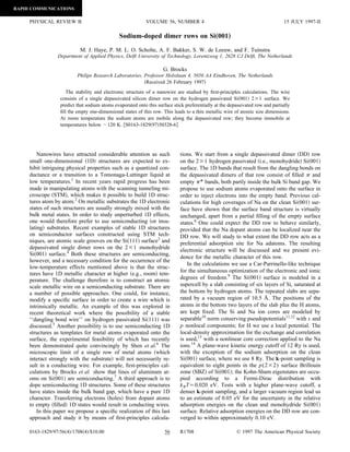
FIG. 1. Adsorption sites on the Si 001 surface. The black FIG. 2. Band structures of the a clean and b the Na covered
circles represent the Si atoms in the top layer of the surface, which 1/4 monolayer Si 001 -p(2 2) surface along with the respective
are arranged in dimer rows along the y direction ; the smaller surface unit cells and Brillouin zones. The Fermi levels E F are
larger circles represent downwards upwards buckled atoms.16 indicated by dashed lines, the shaded areas represent projections of
The c(4 4) unit cell is indicated by the dashed line. The energies the bulk bands. Energies are given with respect to the top of the
for adsorption of one Na atom are given relative to the HH site in bulk valence band.
eV.
within the error bar of the calculation. For diffusion along
Before considering Na adsorption on a DD row, we
the HH-T3 path the activation energy is 0.25 eV. Similar
present results for Na adsorbed on the clean Si 001 surface
high mobilities were also found for other metal atoms ad-
and compare these to recent first-principles calculations of
sorbed on Si 001 , such as aluminum.7
the Na covered Si 001 surface by Kobayashi et al.8 and Ko
The calculated band structure of the clean Si 001 surface
et al.15 In the present work a larger surface unit cell
is shown in Fig. 2 a in a p(2 2) surface cell; it is similar
c(4 4) is used to study adsorption in the low coverage
to that found in previous studies.16 The bonding combina-
regime. We expect that the relative adsorption energies of
tions of the dangling bond surface states are labeled , the
one Na atom in this unit cell are representative for single,
antibonding combinations * and * . The bands are
isolated adsorbed atoms.7 The adsorption energies on the 1 2
filled and in the J and J directions they are largely sur-
clean surface and the corresponding electronic structure
will later be compared to those on the DD row. The clean face resonances, as shown in Fig. 2 a . The * band is1
Si 001 surface is characterized by rows of alternating buck- empty and is a true surface band with a dispersion of 0.76 eV
led Si dimers in the top layer, shown schematically in Fig. 1. in the direction parallel to the dimer row ( J ). Perpendicu-
High-symmetry adsorption sites are labeled by their conven- lar to the rows ( J) its dispersion is 0.15 eV. The empty
tional names see Ref. 8 . The site labeled by HH is lowest * band again is for the most part a surface resonance. In
2
in energy; the T3 and T4 sites represent local minima which Fig. 2 b the band structure is shown for a Si 001 surface on
are approximately 0.1 eV higher in energy. The T3 site is which one Na atom per p(2 2) cell is adsorbed at a HH
located in the middle between the dimer rows and the T4 site site. It is very similar to the band structure of the clean sur-
is slightly displaced 0.23 Å towards the downwards buck- face. The major difference is that the * band is now half
1
led substrate atom. The HB site represents a saddle point on filled, which makes this Na covered surface metallic. The Na
a path over a substrate dimer row in the y direction . It was atoms have transferred their electrons to these * surface
1
located by constraining the adatom to a plane perpendicular states. Similar results were obtained by Kobayashi et al.8 for
to the dimer rows and it is displaced by 0.34 Å with respect the 2 1 Na covered Si 001 surface. In their case the Cou-
to the middle of the dimer row. For all the adsorption sites lomb potential of the Na ions in addition results in a down-
the substrate buckling remains unchanged upon sodium ad- ward shift of the surface bands. For the low coverages which
sorption. Ko et al.15 found for a higher sodium coverage are used here, we find no evidence for such a shift. In the low
that an upward buckling of the substrate dimers towards the coverage regime at least up to 1/4 of a monolayer the shape
trough between two rows leads to a lower energy for the and position of the surface bands with respect to the bulk
adsorption sites in this trough. We therefore recalculated the states remain unaltered. The concentration of Na atoms only
energies of the T3 and T4 configurations using this configu- determines the position of the Fermi level within the fixed
ration for the substrate dimers. The energies of the T3 and * band.
1
T4 relative to the HH site become 0.05 eV and 0.16 eV, Na adsorption at a DD row is modeled in a p(4 2) unit
respectively, and are thus very similar to the ones given in cell, which contains two dimer rows, cf. Fig. 3 a . One of
Fig. 1. The small energy differences between the various these rows is passivated by hydrogen atoms, which results in
adsorption sites indicate that adsorbed Na atoms are highly symmetric surface dimers. The other row represents the DD
mobile at room temperature. The activation energy for diffu- row and consists of p(2 2) buckled Si surface dimers as on
sion in the trough between the dimer rows is negligible, i.e., the clean surface. The adsorption energies at the HH and
3. RAPID COMMUNICATIONS
R1710 M. J. HAYE et al. 56
FIG. 3. a Relative energies for adsorption of a Na atom on a
path along the x direction from the DD row to the hydrogen passi-
vated dimer row, along with the unit cell used in the calculations.
Notation as in Fig. 1; the open circles represent the hydrogen atoms.
The dotted line denotes the corresponding energies for adsorption
on the clean surface. b The corresponding energies and the unit
cell used for adsorption on the monohydride Si 001 surface.
B2 sites on the DD row are equal within the error bar to the
corresponding values at the clean Si 001 surface. We con-
clude that adsorption at a DD row is similar to adsorption at FIG. 4. a Band structure and surface Brillouin zone of the
a dimer row on the clean Si 001 surface. Away from the DD p(4 2) structure shown in Fig. 3 a with one Na atom adsorbed at
row, towards the hydrogen passivated row, energies become the HH site. b and c Plots of the electron density of the * state
1
much higher. This is shown in Fig. 3 a , where we plot rela- at b in a vertical plane perpendicular to the dimer rows through
tive energies for various adsorption sites on a straight line one of the surface dimers, c in a vertical plane along the DD row
between the DD row and the hydrogen passivated row in the passing through the downwards buckled dimer atoms. Si, H, and Na
x direction . Adsorption at the DD row is clearly favorable; atoms are represented by filled, open, and hatched circles, respec-
the DD row traps adsorbing Na atoms. We have checked tively. The contour levels run from 1 to 8 in steps of 1
various other adsorption sites in between the DD and the ( 10 3 a 0 3 ).
passivated row. All of these have energies which are at least
0.3 eV higher than that of the HH site, so the latter is the runs either on top of the DD row, or in between the DD and
most stable adsorption site. Based upon the results of Fig. a neighboring passivated row. The activation energy of the
3 a , an estimate for the activation energy E a for diffusion first path is estimated to be 0.35 eV cf. the energy of the
from the DD row onto the fully passivated surface is 0.9 eV. saddle point HB, see Fig. 1 . A lower bound for the activa-
One can use this value to roughly estimate the jump rate tion energy of the second path is found by a minimization in
for this diffusion event, assuming a simple Arrhenius expres- which we constrain the sodium adatom to a plane perpen-
sion Aexp( Ea /kBT). Using a typical value for the pref- dicular to the dimer rows, through the T4 site. This lower
actor A 1013 Hz and T 300 K, one finds 0.007 Hz, bound is 0.30 eV, which is our final estimate for the energy
which would mean that diffusion from the DD row onto the barrier for diffusion parallel to the DD row. It follows that
passivated surface is a rare event and the Na atom is trapped the Na atoms are mobile along the DD row at room tempera-
at the DD row.17 In order that the DD row can actually ture; at temperatures below 120 K their motion will be
capture Na atoms evaporated onto the surface, these atoms frozen i.e., the jump rate will be much smaller than 1 Hz .
must of course be sufficiently mobile on the hydrogen pas- Having established the stability of a sodium-doped DD
sivated part of the surface. We have calculated energies row, we now consider its electronic structure. The band
along a path from the HH to the T3 site on the monohy- structure of the p(4 2) unit cell with one Na atom adsorbed
dride Si 001 surface, the results of which are shown in Fig. at the HH site, cf. Fig. 3 a , is shown in Fig. 4 a . The
3 b note that for this surface the T3 site is lower in energy surface bands resemble those of the clean surface, cf. Fig. 2;
than the HH site . The activation energy is 0.31 eV, which they result from the dangling bonds of the Si atoms in the
indicates that Na atoms are indeed quite mobile on the pas- DD row. The * state of the DD row is half filled after Na
1
sivated surface estimated jump rate 6 107 Hz . Having adsorption and again the result is similar to Na adsorption on
captured the Na atoms and confined them to the DD row, we the clean surface Fig. 2 b . Hydrogen passivation of the
estimate their mobility along this row. The diffusion path for adjacent row leads to strong covalent bonds between the Si
sodium atoms parallel to the DD row i.e., in the y direction atoms of that row and the H atoms; the energies of the cor-
4. RAPID COMMUNICATIONS
56 SODIUM-DOPED DIMER ROWS ON Si 001 R1711
responding bonding states are well inside the Si bulk valence effect to be much weaker, as the DD states are much more
band. In addition the hydrogen passivated row reduces the extended see Fig. 4 than the GaAs 110 surface states. The
dispersion of the DD surface bands in the direction perpen- electron-lattice interaction can also lead to the opening of a
dicular to the rows ( J, Fig. 4 . The dispersion along J is gap, which is especially likely in quasi-one-dimensional me-
0.02 eV in the p(4 2) cell , as compared to 0.15 eV on the tallic systems where nesting of Fermi surfaces can trigger a
clean surface. So even when separated by only one hydrogen Peierls distortion but does not always have to, according to
passivated row, as in the p(4 2) cell, the surface states of Littlewood and Heine19 . The importance of this effect can
the DD row have a clear 1D character. This is illustrated by be studied within the approximations used here. We have
Figs. 4 b and 4 c which show plots of the * state at .
1 performed a geometry optimization using a p(4 4) unit cell
This state has antibonding character between the Si atoms of with two Na atoms adsorbed at HH sites, i.e., the unit cell of
one depassivated dimer; it has p z character on the down- Fig. 3 a doubled in the direction of the dimer rows. We
wards buckled Si atom and an s p 3 -like lobe on the upwards found no evidence for a spontaneous breaking of the trans-
buckled atom which reflects the s p 2 - and s p 3 -like hybrid- lational symmetry and no corresponding opening of a gap at
izations of the down- and upwards buckled dimer atoms, the Fermi level.
respectively . Clearly, this state is one dimensional. In conclusion we have shown that a depassivated dimer
Within the approximations used our calculations predict DD row on the monohydride Si 001 surface acts as an
that the Na-doped DD row has metallic properties. We adsorption template for Na atoms. At room temperature the
briefly speculate on additional effects which could open a sodium atoms are sufficiently mobile to reach the DD row
gap and destroy the metallicity of this structure. If the on-site and subsequently become trapped at this row. The adatoms
coulomb correlation energy becomes large as compared to are still mobile along this row, but at a temperature below
the width of the surface band, the system could become a 120 K their motion is completely frozen. The Na atoms
Mott-Hubbard insulator. The on-site correlation has been transfer their electrons to the empty one-dimensional band of
used in describing the electronic structure of the Na covered the DD row. A partial filling of this band leads to a one-
GaAs 110 surface.18 For the present system we expect this dimensional metallic atomic wire.
1 13
See, e.g., G.D. Mahan, Many-particle Physics Plenum, New J. P. Perdew and A. Zunger, Phys. Rev. B 23, 5048 1981 .
14
York, 1990 . S. G. Louie, S. Froyen, and M. L. Cohen, Phys. Rev. B 26, 1738
2
M. F. Crommie, C. P. Lutz, and D. M. Eigler, Science 262, 218 1982 .
1993 . 15
Y.-J. Ko, K. J. Chang, and J.-Y. Yi, Phys. Rev. B 51, 4329
3
Q. J. Gu et al., Appl. Phys. Lett. 66, 1747 1995 . 1995 .
4
T.-C. Shen et al., Science 268, 1590 1995 . 16
A. Ramstad, G. Brocks, and P. J. Kelly, Phys. Rev. B 51, 14 504
5
S. Watanabe et al., Phys. Rev. B 52, 10 768 1995 . 1995 , and references therein.
6
T.-C. Shen, C. Wang, and J. R. Tucker, Phys. Rev. Lett. 78, 1271 17
Jump rates can only be given as order-of-magnitude estimates.
1997 . Allowing for uncertainties in the activation energy or prefactor
7
G. Brocks, P. J. Kelly, and R. Car, Phys. Rev. Lett. 70, 2786 could, for instance, make the jump rate two orders of magnitude
1993 ; J. Vac. Sci. Technol. B 12, 2705 1994 .
8 higher. Experimentally one has a finer control over the jump
K. Kobayashi et al., Phys. Rev. B 45, 3469 1992 .
9 rate; instead of performing the experiment at room temperature,
R. Car and M. Parrinello, Phys. Rev. Lett. 55, 2471 1985 .
10 cooling down by 40 K decreases the jump rate by two orders
L. Kleinman and D. M. Bylander, Phys. Rev. Lett. 48, 1425
of magnitude.
1982 . 18
11 ¨ J. Hebenstreit and M. Scheffler, Phys. Rev. B 46, 10 134 1992 ;
G. B. Bachelet, D. R. Hamann, and M. Schluter, Phys. Rev. B 26,
4199 1982 . O. Pankratov and M. Scheffler, Phys. Rev. Lett. 70, 351 1993 .
19
12
N. Troullier and J. L. Martins, Phys. Rev. B 43, 1993 1991 . P. B. Littlewood and V. Heine, J. Phys. C 14, 2943 1981 .