SlideShare uma empresa Scribd logo
1 de 24
Baixar para ler offline
a                                                                           RF PLL Frequency Synthesizers
                                                                     ADF4110/ADF4111/ADF4112/ADF4113
   FEATURES                                                                          GENERAL DESCRIPTION
   ADF4110: 550 MHz                                                                  The ADF4110 family of frequency synthesizers can be used
   ADF4111: 1.2 GHz                                                                  to implement local oscillators in the upconversion and down-
   ADF4112: 3.0 GHz                                                                  conversion sections of wireless receivers and transmitters. They
   ADF4113: 4.0 GHz                                                                  consist of a low-noise digital PFD (Phase Frequency Detector),
   2.7 V to 5.5 V Power Supply                                                       a precision charge pump, a programmable reference divider,
   Separate Charge Pump Supply (VP) Allows Extended                                  programmable A and B counters and a dual-modulus prescaler
     Tuning Voltage in 3 V Systems                                                   (P/P + 1). The A (6-bit) and B (13-bit) counters, in conjunction
   Programmable Dual Modulus Prescaler 8/9, 16/17,                                   with the dual modulus prescaler (P/P + 1), implement an N
     32/33, 64/65                                                                    divider (N = BP + A). In addition, the 14-bit reference counter
   Programmable Charge Pump Currents                                                 (R Counter), allows selectable REFIN frequencies at the PFD
   Programmable Antibacklash Pulsewidth                                              input. A complete PLL (Phase-Locked Loop) can be imple-
   3-Wire Serial Interface                                                           mented if the synthesizer is used with an external loop filter and
   Analog and Digital Lock Detect                                                    VCO (Voltage Controlled Oscillator).
   Hardware and Software Power-Down Mode                                             Control of all the on-chip registers is via a simple 3-wire interface.
   APPLICATIONS                                                                      The devices operate with a power supply ranging from 2.7 V to
   Base Stations for Wireless Radio (GSM, PCS, DCS,                                  5.5 V and can be powered down when not in use.
     CDMA, WCDMA)
   Wireless Handsets (GSM, PCS, DCS, CDMA, WCDMA)
   Wireless LANS
   Communications Test Equipment
   CATV Equipment
                                                               FUNCTIONAL BLOCK DIAGRAM
                                        AVDD           DVDD                              VP      CPGND                               RSET


                                                                                                                   REFERENCE


                                                                    14-BIT
              REFIN                                              R COUNTER                      PHASE
                                                                                              FREQUENCY                CHARGE
                                                                                               DETECTOR                 PUMP                CP
                                                                          14

                                                                 R COUNTER
                                                                   LATCH

               CLK
                                      24-BIT                      FUNCTION
              DATA                INPUT REGISTER                   LATCH                        LOCK         CURRENT          CURRENT
                                                       22
                LE                                                                             DETECT        SETTING 1        SETTING 2

                                                                A, B COUNTER
                                               SDOUT                LATCH                                  CPI3 CPI2 CPI1 CPI6 CPI5 CPI4
                                                                               19


                                        FROM                                                                                     HIGH Z
                                      FUNCTION
                                       LATCH
                                                                                                    AVDD
                                                                     13
                                                                                                                 MUX                        MUXOUT
                                               N = BP + A
                                                                  13-BIT
                                                               B COUNTER
                                                                                                   SDOUT
              RFINA                                           LOAD
                                     PRESCALER
                                       P/P +1                 LOAD
              RFINB
                                                                  6-BIT
                                                               A COUNTER                                    M3   M2      M1

                                                                                    ADF4110/ADF4111
                                                                     6
                                                                                    ADF4112/ADF4113


                           CE         AGND              DGND

REV. A
Information furnished by Analog Devices is believed to be accurate and
reliable. However, no responsibility is assumed by Analog Devices for its
use, nor for any infringements of patents or other rights of third parties           One Technology Way, P.O. Box 9106, Norwood, MA 02062-9106, U.S.A.
which may result from its use. No license is granted by implication or               Tel: 781/329-4700   World Wide Web Site: http://www.analog.com
otherwise under any patent or patent rights of Analog Devices.                       Fax: 781/326-8703                     © Analog Devices, Inc., 2001
ADF4110/ADF4111/ADF4112/ADF4113–SPECIFICATIONS1T = T
(AV = DV = 3 V 10%, 5 V 10%; AV ≤ V ≤ 6.0 V; AGND = DGND = CPGND = 0 V; R = 4.7 k ; dBm referred to 50 ;
  DD     DD                         DD    P                                   SET                            A   MIN to TMAX   unless
otherwise noted.)
Parameter                                B Version    B Chips2       Unit           Test Conditions/Comments
RF CHARACTERISTICS (3 V)                                                            See Figure 3 for Input Circuit.
 RF Input Frequency                                                                 Use a square wave for lower frequencies,
   ADF4110                               80/550       80/550         MHz min/max    below the minimum level stated.
   ADF4110                               50/550       50/550         MHz min/max    Input Level = –10 dBm
   ADF4111                               0.08/1.2     0.08/1.2       GHz min/max
   ADF4112                               0.2/3.0      0.2/3.0        GHz min/max
   ADF4112                               0.1/3.0      0.1/3.0        GHz min/max    Input Level = –10 dBm
   ADF4113                               0.2/3.7      0.2/3.7        GHz min/max    Input Level = –10 dBm
 RF Input Sensitivity                    –15/0        –15/0          dBm min/max
 Maximum Allowable Prescaler
 Output Frequency3                       165          165            MHz max
RF CHARACTERISTICS (5 V)
 RF Input Frequency                                                                 Use a square wave for lower frequencies,
   ADF4110                               80/550       80/550         MHz min/max    below the minimum level stated.
   ADF4111                               0.08/1.4     0.08/1.4       GHz min/max
   ADF4112                               0.1/3.0      0.1/3.0        GHz min/max
   ADF4113                               0.2/3.7      0.2/3.7        GHz min/max
   ADF4113                               0.2/4.0      0.2/4.0        GHz min/max    Input Level = –5 dBm
 RF Input Sensitivity                    –10/0        –10/0          dBm min/max
 Maximum Allowable Prescaler
 Output Frequency3                       200          200            MHz max
REFIN CHARACTERISTICS
 REFIN Input Frequency                   5/100        5/100          MHz min/max    For f < 5 MHz, use dc-coupled square
                                                                                    wave, (0 to VDD).
  Reference Input Sensitivity4           –5           –5             dBm min        AC-Coupled. When DC-Coupled:
                                                                                    0 to VDD max (CMOS-Compatible)
  REFIN Input Capacitance                10           10             pF max
  REFIN Input Current                    ± 100        ± 100          µA max
PHASE DETECTOR
 Phase Detector Frequency5               55           55             MHz max
CHARGE PUMP
 ICP Sink/Source                                                                    Programmable: See Table V
   High Value                            5            5              mA typ         With RSET = 4.7 kΩ
   Low Value                             625          625            µA typ
   Absolute Accuracy                     2.5          2.5            % typ          With RSET = 4.7 kΩ
   RSET Range                            2.7/10       2.7/10         kΩ typ         See Table V
 ICP 3-State Leakage Current             1            1              nA typ
 Sink and Source Current Matching        2            2              % typ          0.5 V ≤ VCP ≤ VP – 0.5
 ICP vs. VCP                             1.5          1.5            % typ          0.5 V ≤ VCP ≤ VP – 0.5
 ICP vs. Temperature                     2            2              % typ          VCP = VP/2
LOGIC INPUTS
 VINH, Input High Voltage                0.8 × DVDD   0.8 × DVDD     V min
 VINL, Input Low Voltage                 0.2 × DVDD   0.2 × DVDD     V max
 IINH/IINL, Input Current                ±1           ±1             µA max
 CIN, Input Capacitance                  10           10             pF max
LOGIC OUTPUTS
 VOH, Output High Voltage                DVDD – 0.4   DVDD – 0.4     V min          IOH = 500 µA
 VOL, Output Low Voltage                 0.4          0.4            V max          IOL = 500 µA
POWER SUPPLIES
 AVDD                                    2.7/5.5      2.7/5.5        V min/V max
 DVDD                                    AVDD         AVDD
 VP                                      AVDD/6.0     AVDD/6.0       V min/V max    AVDD ≤ VP ≤ 6.0 V
 IDD6 (AIDD + DIDD )                                                                See TPCs 21a and 21b
   ADF4110                               5.5          4.5            mA max         4.5 mA Typical
   ADF4111                               5.5          4.5            mA max         4.5 mA Typical
   ADF4112                               7.5          6.5            mA max         6.5 mA Typical
   ADF4113                               11           8.5            mA max         8.5 mA Typical
   IP                                    0.5          0.5            mA max         TA = 25°C
 Low Power Sleep Mode                    1            1              µA typ
                                                               –2–                                                       REV. A
ADF4110/ADF4111/ADF4112/ADF4113
Parameter                                             B Version           B Chips2            Unit                   Test Conditions/Comments
NOISE CHARACTERISTICS
 ADF4113 Phase Noise Floor 7                          –171                –171                dBc/Hz typ             @ 25 kHz PFD Frequency
                                                      –164                –164                dBc/Hz typ             @ 200 kHz PFD Frequency
     Phase Noise Performance8                                                                                        @ VCO Output
       ADF4110: 540 MHz Output9                       –91                 –91                 dBc/Hz typ             @ 1 kHz Offset and 200 kHz PFD Frequency
       ADF4111: 900 MHz Output10                      –87                 –87                 dBc/Hz typ             @ 1 kHz Offset and 200 kHz PFD Frequency
       ADF4112: 900 MHz Output10                      –90                 –90                 dBc/Hz typ             @ 1 kHz Offset and 200 kHz PFD Frequency
       ADF4113: 900 MHz Output10                      –91                 –91                 dBc/Hz typ             @ 1 kHz Offset and 200 kHz PFD Frequency
       ADF4111: 836 MHz Output11                      –78                 –78                 dBc/Hz typ             @ 300 Hz Offset and 30 kHz PFD Frequency
       ADF4112: 1750 MHz Output 12                    –86                 –86                 dBc/Hz typ             @ 1 kHz Offset and 200 kHz PFD Frequency
       ADF4112: 1750 MHz Output 13                    –66                 –66                 dBc/Hz typ             @ 200 Hz Offset and 10 kHz PFD Frequency
       ADF4112: 1960 MHz Output 14                    –84                 –84                 dBc/Hz typ             @ 1 kHz Offset and 200 kHz PFD Frequency
       ADF4113: 1960 MHz Output 14                    –85                 –85                 dBc/Hz typ             @ 1 kHz Offset and 200 kHz PFD Frequency
       ADF4113: 3100 MHz Output 15                    –86                 –86                 dBc/Hz typ             @ 1 kHz Offset and 1 MHz PFD Frequency
     Spurious Signals
       ADF4110: 540 MHz Output9                       –97/–106            –97/–106            dBc typ                @ 200 kHz/400 kHz and 200 kHz PFD Frequency
       ADF4111: 900 MHz Output10                      –98/–110            –98/–110            dBc typ                @ 200 kHz/400 kHz and 200 kHz PFD Frequency
       ADF4112: 900 MHz Output10                      –91/–100            –91/–100            dBc typ                @ 200 kHz/400 kHz and 200 kHz PFD Frequency
       ADF4113: 900 MHz Output10                      –100/–110           –100/–110           dBc typ                @ 200 kHz/400 kHz and 200 kHz PFD Frequency
       ADF4111: 836 MHz Output11                      –81/–84             –81/–84             dBc typ                @ 30 kHz/60 kHz and 30 kHz PFD Frequency
       ADF4112: 1750 MHz Output 12                    –88/–90             –88/–90             dBc typ                @ 200 kHz/400 kHz and 200 kHz PFD Frequency
       ADF4112: 1750 MHz Output 13                    –65/–73             –65/–73             dBc typ                @ 10 kHz/20 kHz and 10 kHz PFD Frequency
       ADF4112: 1960 MHz Output 14                    –80/–84             –80/–84             dBc typ                @ 200 kHz/400 kHz and 200 kHz PFD Frequency
       ADF4113: 1960 MHz Output 14                    –80/–84             –80/–84             dBc typ                @ 200 kHz/400 kHz and 200 kHz PFD Frequency
       ADF4113: 3100 MHz Output15                     –80/–82             –82/–82             dBc typ                @ 1 MHz/2 MHz and 1 MHz PFD Frequency
NOTES
 1
   Operating temperature range is as follows: B Version: –40°C to +85°C.
 2
   The B Chip specifications are given as typical values.
 3
   This is the maximum operating frequency of the CMOS counters. The prescaler value should be chosen to ensure that the RF input is divided down to a frequency
   which is less than this value.
 4
   AVDD = DVDD = 3 V; For AVDD = DVDD = 5 V, use CMOS-compatible levels.
 5
   Guaranteed by design.
 6
   TA = 25°C; AVDD = DVDD = 3 V; P = 16; SYNC = 0; DLY = 0; RFIN for ADF4110 = 540 MHz; RFIN for ADF4111, ADF4112, ADF4113 = 900 MHz.
 7
   The synthesizer phase noise floor is estimated by measuring the in-band phase noise at the output of the VCO and subtracting 20 logN (where N is the N divider value).
 8
   The phase noise is measured with the EVAL-ADF411XEB1 Evaluation Board and the HP8562E Spectrum Analyzer. The spectrum analyzer provides the REFIN for
    the synthesizer (fREFOUT = 10 MHz @ 0 dBm). SYNC = 0; DLY = 0 (See Table III).
 9
   fREFIN = 10 MHz; fPFD = 200 kHz; Offset frequency = 1 kHz; fRF = 540 MHz; N = 2700; Loop B/W = 20 kHz.
10
   fREFIN = 10 MHz; fPFD = 200 kHz; Offset frequency = 1 kHz; fRF = 900 MHz; N = 4500; Loop B/W = 20 kHz.
11
   fREFIN = 10 MHz; fPFD = 30 kHz; Offset frequency = 300 Hz; fRF = 836 MHz; N = 27867; Loop B/W = 3 kHz.
12
   fREFIN = 10 MHz; fPFD = 200 kHz; Offset frequency = 1 kHz; fRF = 1750 MHz; N = 8750; Loop B/W = 20 kHz.
13
   fREFIN = 10 MHz; fPFD = 10 kHz; Offset frequency = 200 Hz; fRF = 1750 MHz; N = 175000; Loop B/W = 1 kHz.
14
   fREFIN = 10 MHz; fPFD = 200 kHz; Offset frequency = 1 kHz; fRF = 1960 MHz; N = 9800; Loop B/W = 20 kHz.
15
   fREFIN = 10 MHz; fPFD = 1 MHz; Offset frequency = 1 kHz; fRF = 3100 MHz; N = 3100; Loop B/W = 20 kHz.
Specifications subject to change without notice.


                                                        (AVDD = DVDD = 3 V 10%, 5 V 10%; AVDD ≤ VP ≤ 6.0 V; AGND = DGND = CPGND = 0 V;
TIMING CHARACTERISTICS1 R                                 SET = 4.7 k ; TA = TMIN to TMAX unless otherwise noted.)

                                         Limit at TMIN to TMAX
Parameter                                (B Version)                                             Unit                                 Test Conditions/Comments
t1                                       10                                                      ns min                               DATA to CLOCK Setup Time
t2                                       10                                                      ns min                               DATA to CLOCK Hold Time
t3                                       25                                                      ns min                               CLOCK High Duration
t4                                       25                                                      ns min                               CLOCK Low Duration
t5                                       10                                                      ns min                               CLOCK to LE Setup Time
t6                                       20                                                      ns min                               LE Pulsewidth
NOTES
1
 Guaranteed by design but not production tested.
Specifications subject to change without notice.


REV. A                                                                                  –3–
ADF4110/ADF4111/ADF4112/ADF4113
                                                                                 t3          t4

                 CLOCK


                                                t1          t2

                                                                                                        DB1                      DB0 (LSB)
                  DATA         DB20 (MSB)            DB19                   DB2                   (CONTROL BIT C2)            (CONTROL BIT C1)

                                                                                                                                              t6

                      LE


                                                                                                                                       t5

                      LE


                                                                 Figure 1. Timing Diagram


ABSOLUTE MAXIMUM RATINGS 1, 2                                                          CSP θJA Thermal Impedance (Paddle Soldered) . . . 122°C/W
(TA = 25°C unless otherwise noted)                                                     CSP θJA Thermal Impedance
AVDD to GND3 . . . . . . . . . . . . . . . . . . . . . . . . –0.3 V to +7 V              (Paddle Not Soldered) . . . . . . . . . . . . . . . . . . . . . 216°C/W
AVDD to DVDD . . . . . . . . . . . . . . . . . . . . . . –0.3 V to +0.3 V              Lead Temperature, Soldering
VP to GND . . . . . . . . . . . . . . . . . . . . . . . . . . . –0.3 V to +7 V           Vapor Phase (60 sec) . . . . . . . . . . . . . . . . . . . . . . . . 215°C
VP to AVDD . . . . . . . . . . . . . . . . . . . . . . . . . –0.3 V to +5.5 V            Infrared (15 sec) . . . . . . . . . . . . . . . . . . . . . . . . . . . . 220°C
Digital I/O Voltage to GND . . . . . . . . –0.3 V to VDD + 0.3 V                       NOTES
                                                                                       1
Analog I/O Voltage to GND . . . . . . . . . –0.3 V to VP + 0.3 V                         Stresses above those listed under Absolute Maximum Ratings may cause perma-
REFIN, RFINA, RFINB to GND . . . . . . –0.3 V to VDD + 0.3 V                             nent damage to the device. This is a stress rating only; functional operation of the
                                                                                         device at these or any other conditions above those listed in the operational
RFINA to RFINB . . . . . . . . . . . . . . . . . . . . . . . . . . . ± 320 mV            sections of this specification is not implied. Exposure to absolute maximum rating
Operating Temperature Range                                                              conditions for extended periods may affect device reliability.
                                                                                       2
  Industrial (B Version) . . . . . . . . . . . . . . . –40°C to +85°C                    This device is a high-performance RF integrated circuit with an ESD rating of
Storage Temperature Range . . . . . . . . . . . . –65°C to +150°C                        < 2 kV and it is ESD sensitive. Proper precautions should be taken for handling
                                                                                         and assembly.
Maximum Junction Temperature . . . . . . . . . . . . . . . . 150°C                     3
                                                                                         GND = AGND = DGND = 0 V.
TSSOP θJA Thermal Impedance . . . . . . . . . . . . . 150.4°C/W
                                                                                       TRANSISTOR COUNT
                                                                                       6425 (CMOS) and 303 (Bipolar).


CAUTION
ESD (electrostatic discharge) sensitive device. Electrostatic charges as high as 4000 V readily accumu-
late on the human body and test equipment and can discharge without detection. Although the                                          WARNING!
ADF4110/ADF4111/ADF4112/ADF4113 features proprietary ESD protection circuitry, permanent
damage may occur on devices subjected to high-energy electrostatic discharges. Therefore, proper ESD
                                                                                                                                                    ESD SENSITIVE DEVICE
precautions are recommended to avoid performance degradation or loss of functionality.


                                                                    ORDERING GUIDE

Model                           Temperature Range                    Package Description                                                           Package Option*
ADF4110BRU                      –40°C to +85°C                       Thin Shrink Small Outline Package (TSSOP)                                     RU-16
ADF4110BCP                      –40°C to +85°C                       Chip Scale Package (CSP)                                                      CP-20
ADF4111BRU                      –40°C to +85°C                       Thin Shrink Small Outline Package (TSSOP)                                     RU-16
ADF4111BCP                      –40°C to +85°C                       Chip Scale Package (CSP)                                                      CP-20
ADF4112BRU                      –40°C to +85°C                       Thin Shrink Small Outline Package (TSSOP)                                     RU-16
ADF4112BCP                      –40°C to +85°C                       Chip Scale Package (CSP)                                                      CP-20
ADF4113BRU                      –40°C to +85°C                       Thin Shrink Small Outline Package (TSSOP)                                     RU-16
ADF4113BCP                      –40°C to +85°C                       Chip Scale Package (CSP)                                                      CP-20
ADF4113BCHIPS                   –40°C to +85°C                       DICE                                                                          DICE
*Contact the factory for chip availability.


                                                                                 –4–                                                                              REV. A
ADF4110/ADF4111/ADF4112/ADF4113
                                                  PIN FUNCTION DESCRIPTIONS

Pin No.   Mnemonic       Function
1         RSET           Connecting a resistor between this pin and CPGND sets the maximum charge pump output current. The
                         nominal voltage potential at the RSET pin is 0.56 V. The relationship between ICP and RSET is
                                                                      23.5
                                                          ICP max =
                                                                      RSET
                        So, with RSET = 4.7 kΩ, ICPmax = 5 mA.
2         CP            Charge Pump Output. When enabled this provides ±ICP to the external loop filter, which in turn drives the
                        external VCO.
3         CPGND         Charge Pump Ground. This is the ground return path for the charge pump.
4         AGND          Analog Ground. This is the ground return path of the prescaler.
5         RFINB         Complementary Input to the RF Prescaler. This point should be decoupled to the ground plane with
                        a small bypass capacitor, typically 100 pF. See Figure 3.
6         RFINA         Input to the RF Prescaler. This small signal input is ac-coupled from the VCO.
7         AVDD          Analog Power Supply. This may range from 2.7 V to 5.5 V. Decoupling capacitors to the analog ground
                        plane should be placed as close as possible to this pin. AVDD must be the same value as DVDD.
8         REFIN         Reference Input. This is a CMOS input with a nominal threshold of VDD/2 and an equivalent input resis-
                        tance of 100 kΩ. See Figure 2. This input can be driven from a TTL or CMOS crystal oscillator or it
                        can be ac-coupled.
9         DGND          Digital Ground.
10        CE            Chip Enable. A logic low on this pin powers down the device and puts the charge pump output into three-
                        state mode. Taking the pin high will power up the device depending on the status of the power-down bit F2.
11        CLK           Serial Clock Input. This serial clock is used to clock in the serial data to the registers. The data is latched into
                        the 24-bit shift register on the CLK rising edge. This input is a high impedance CMOS input.
12        DATA          Serial Data Input. The serial data is loaded MSB first with the two LSBs being the control bits. This
                        input is a high impedance CMOS input.
13        LE            Load Enable, CMOS Input. When LE goes high, the data stored in the shift registers is loaded into one
                        of the four latches, the latch being selected using the control bits.
14        MUXOUT        This multiplexer output allows either the Lock Detect, the scaled RF or the scaled Reference Frequency
                        to be accessed externally.
15        DVDD          Digital Power Supply. This may range from 2.7 V to 5.5 V. Decoupling capacitors to the digital ground
                        plane should be placed as close as possible to this pin. DVDD must be the same value as AVDD.
16        VP            Charge Pump Power Supply. This should be greater than or equal to VDD. In systems where VDD is 3 V,
                        it can be set to 6 V and used to drive a VCO with a tuning range of up to 6 V.

                                                      PIN CONFIGURATIONS


                               TSSOP                                                          CHIP SCALE PACKAGE
                                                                                                                                      17 DVDD

                                                                                                                                                16 DVDD
                                                                                                                  19 RSET


                     RSET 1               16 VP
                                                                                                        20 CP


                                                                                                                            18 VP


                       CP 2               15 DVDD
                               ADF4110
                   CPGND 3     ADF4111    14 MUXOUT                                        CPGND    1                                                     15 MUXOUT
                               ADF4112                                                                            ADF4110
                     AGND 4    ADF4113    13 LE                                             AGND    2             ADF4111                                 14 LE
                               TOP VIEW 12 DATA
                                                                                                                  ADF4112
                     RFINB 5                                                                AGND    3                                                     13 DATA
                             (Not to Scale)                                                                       ADF4113
                     RFINA 6                11 CLK
                                                                                            RFINB   4              TOP VIEW                               12 CLK
                                                                                                                 (Not to Scale)
                     AVDD 7               10 CE
                                                                                            RFINA   5                                                     11 CE
                     REFIN 8              9   DGND
                                                                                                                                                DGND 10
                                                                                                        AVDD 6

                                                                                                                  AVDD 7

                                                                                                                            REFIN 8
                                                                                                                                      DGND 9


REV. A                                                           –5–
ADF4110/ADF4111/ADF4112/ADF4113
                                                                                                                                          0
                                  FREQ-UNIT PARAM-TYPE DATA-FORMAT KEYWORD        IMPEDANCE – OHMS                                                      REFERENCE            VDD = 3V, VP = 5V
                                    GHz        S           MA          R                 50                                             –10
                                                                                                                                                        LEVEL = –4.2dBm      ICP = 5mA
                                  FREQ   MAGS11            ANGS11    FREQ   MAGS11         ANGS11                                       –20                                  PFD FREQUENCY = 200kHz
                                  0.05   0.89207           –2.0571   1.05   0.9512         –40.134                                                                           LOOP BANDWIDTH = 20kHz
                                  0.10   0.8886            –4.4427   1.10   0.93458        –43.747


                                                                                                                    OUTPUT POWER – dB
                                  0.15   0.89022           –6.3212   1.15   0.94782        –44.393                                      –30                                  RES. BANDWIDTH = 10Hz
                                  0.20   0.96323           –2.1393   1.20   0.96875        –46.937                                                                           VIDEO BANDWIDTH = 10Hz
                                  0.25   0.90566           –12.13    1.25   0.92216        –49.6                                                                             SWEEP = 1.9 SECONDS
                                  0.30   0.90307           –13.52    1.30   0.93755        –51.884
                                                                                                                                        –40
                                  0.35   0.89318           –15.746   1.35   0.96178        –51.21                                                                            AVERAGES = 19
                                  0.40   0.89806           –18.056   1.40   0.94354        –53.55                                       –50
                                  0.45   0.89565           –19.693   1.45   0.95189        –56.786
                                  0.50   0.88538           –22.246   1.50   0.97647        –58.781
                                  0.55   0.89699           –24.336   1.55   0.98619        –60.545                                      –60
                                  0.60   0.89927           –25.948   1.60   0.95459        –61.43
                                  0.65   0.87797           –28.457   1.65   0.97945        –61.241
                                  0.70   0.90765           –29.735   1.70   0.98864        –64.051                                      –70                                          –92.5dBc/Hz
                                  0.75   0.88526           –31.879   1.75   0.97399        –66.19
                                  0.80   0.81267           –32.681   1.80   0.97216        –63.775
                                  0.85   0.90357           –31.522                                                                      –80
                                  0.90   0.92954           –34.222
                                  0.95   0.92087           –36.961                                                                      –90
                                  1.00   0.93788           –39.343

                                                                                                                                      –100
                                                                                                                                                –2kHz       –1kHz      900MHz        +1kHz     +2kHz

TPC 1. S-Parameter Data for the ADF4113 RF Input (Up                                                                   TPC 4. ADF4113 Phase Noise (900 MHz, 200 kHz,
to 1.8 GHz)                                                                                                            20 kHz) with DLY and SYNC Enabled


                                                                                                                   10dB/DIVISION                                    RL = –40dBc/Hz            RMS NOISE = 0.52
                          0                                                                                           –40

                                                                                  VDD = 3V                                              –50
                         –5
                                                                                  VP = 3V
                                                                                                                                        –60
                                                                                                                                                                                        0.52 rms
 RF INPUT POWER – dBm


                        –10
                                                                                                               PHASE NOISE – dBc/Hz
                                                                                                                                        –70

                                                                                                                                        –80
                        –15
                                                                                                                                        –90
                        –20                           TA = +85 C
                                                                                                                                      –100
                                                                     TA = +25 C
                        –25                                                                                                           –110

                                                                                                                                      –120
                        –30
                                                                                                                                      –130
                                                       TA = –40 C
                        –35                                                                                                           –140
                              0              1            2        3                  4              5
                                                                                                                                        100Hz       FREQUENCY OFFSET FROM 900MHz CARRIER               1MHz
                                                   RF INPUT FREQUENCY – GHz

                                      TPC 2. Input Sensitivity (ADF4113)                                       TPC 5. ADF4113 Integrated Phase Noise (900 MHz,
                                                                                                               200 kHz, 20 kHz, Typical Lock Time: 400 µ s)


                                                                                                                     10dB/DIVISION                                  RL = –40dBc/Hz             RMS NOISE = 0.62
                          0                                                                                            –40
                                            REFERENCE                VDD = 3V, VP = 5V
                        –10                                                                                                             –50
                                            LEVEL = –4.2dBm          ICP = 5mA
                        –20                                          PFD FREQUENCY = 200kHz                                             –60
                                                                     LOOP BANDWIDTH = 20kHz                                                                                             0.62 rms
                                                                                                               PHASE NOISE – dBc/Hz
    OUTPUT POWER – dB


                        –30                                          RES. BANDWIDTH = 10Hz                                              –70
                                                                     VIDEO BANDWIDTH = 10Hz
                        –40                                          SWEEP = 1.9 SECONDS                                                –80
                                                                     AVERAGES = 19
                        –50                                                                                                             –90

                        –60                                                                                                           –100

                        –70                                                  –91.0dBc/Hz                                              –110

                        –80                                                                                                           –120

                        –90                                                                                                           –130

                        –100                                                                                                          –140
                                    –2kHz          –1kHz       900MHz       +1kHz         +2kHz                                         100Hz       FREQUENCY OFFSET FROM 900MHz CARRIER               1MHz

     TPC 3. ADF4113 Phase Noise (900 MHz, 200 kHz, 20 kHz)                                                     TPC 6. ADF4113 Integrated Phase Noise (900 MHz,
                                                                                                               200 kHz, 35 kHz, Typical Lock Time: 200 µ s)


                                                                                                         –6–                                                                                              REV. A
ADF4110/ADF4111/ADF4112/ADF4113
                                                                                                     10dB/DIVISION                                       RL = –40dBc/Hz                RMS NOISE = 1.6
                           0                                                                           –40
                                        REFERENCE             VDD = 3V, VP = 5V
                         –10            LEVEL = –4.2dBm                                                                     –50
                                                              ICP = 5mA
                         –20                                  PFD FREQUENCY = 200kHz                                        –60
                                                              LOOP BANDWIDTH = 20kHz


                                                                                                PHASE NOISE – dBc/Hz
                                                              RES. BANDWIDTH = 1kHz                                         –70
     OUTPUT POWER – dB


                         –30
                                                              VIDEO BANDWIDTH = 1kHz                                                                                      1.6 rms
                         –40                                  SWEEP = 2.5 SECONDS                                           –80
                                                              AVERAGES = 30
                         –50                                                                                                –90

                         –60                                                                                           –100

                         –70                                                                                           –110

                         –80                                         –90.2dBc                                          –120

                         –90                                                                                           –130

                        –100                                                                                           –140
                               –400kHz      –200kHz       900MHz   +200kHz      +400kHz                                  100Hz         FREQUENCY OFFSET FROM 1750MHz CARRIER                 1MHz

  TPC 7. ADF4113 Reference Spurs (900 MHz, 200 kHz,                                             TPC 10. ADF4113 Integrated Phase Noise (1750 MHz,
  20 kHz)                                                                                       30 kHz, 3 kHz)


                           0                                                                                                  0
                                                                                                                                                                  VDD = 3V, VP = 5V
                                        REFERENCE             VDD = 3V, VP = 5V                                                             REFERENCE
                         –10            LEVEL = –4.2dBm                                                                     –10             LEVEL = –5.7dBm       ICP = 5mA
                                                              ICP = 5mA
                                                                                                                                                                  PFD FREQUENCY = 30kHz
                                                              PFD FREQUENCY = 200kHz
                         –20                                                                                                –20                                   LOOP BANDWIDTH = 3kHz
                                                              LOOP BANDWIDTH = 35kHz
                                                                                                                                                                  RES. BANDWIDTH = 3Hz
                                                              RES. BANDWIDTH = 1kHz
                                                                                                     POWER OUTPUT – dB
                                                                                                                            –30
    OUTPUT POWER – dB


                         –30                                                                                                                                      VIDEO BANDWIDTH = 3Hz
                                                              VIDEO BANDWIDTH = 1kHz
                                                                                                                                                                  SWEEP = 255 SECONDS
                         –40                                  SWEEP = 2.5 SECONDS                                           –40                                   POSITIVE PEAK DETECT
                                                              AVERAGES = 30
                                                                                                                                                                  MODE
                         –50                                                                                                –50

                         –60                                                                                                –60

                         –70                                                                                                –70                                             –79.6dBc

                         –80                                         –89.3dBc                                               –80

                         –90                                                                                                –90

                  –100                                                                                                   –100
                               –400kHz     –200kHz    900MHz       +200kHz      +400kHz                                            –80kHz       –40kHz      1750MHz       +40kHz       +80kHz


  TPC 8. ADF4113 Reference Spurs (900 MHz, 200 kHz,                                             TPC 11. ADF4113 Reference Spurs (1750 MHz, 30 kHz,
  35 kHz)                                                                                       3 kHz)


                           0                                                                                                  0
                                        REFERENCE             VDD = 3V, VP = 5V                                                             REFERENCE            VDD = 3V, VP = 5V
                         –10            LEVEL = –8.0dBm       ICP = 5mA                                                     –10             LEVEL = –4.2dBm      ICP = 5mA
                                                              PFD FREQUENCY = 30kHz                                                                              PFD FREQUENCY = 1MHz
                         –20                                                                                                –20                                  LOOP BANDWIDTH = 100kHz
                                                              LOOP BANDWIDTH = 3kHz
                                                              RES. BANDWIDTH = 10kHz                                                                             RES. BANDWIDTH = 10Hz
    OUTPUT POWER – dB


                         –30
                                                                                                        OUTPUT POWER – dB


                                                                                                                            –30
                                                              VIDEO BANDWIDTH = 10kHz                                                                            VIDEO BANDWIDTH = 10Hz
                                                              SWEEP = 477ms                                                                                      SWEEP = 1.9 SECONDS
                         –40                                                                                                –40
                                                              AVERAGES = 10                                                                                      AVERAGES = 45
                         –50                                                                                                –50

                         –60                                                                                                –60
                                                                                                                                                                           –86.6dBc/Hz
                         –70                                                                                                –70

                         –80                                –75.2dBc/Hz                                                     –80

                         –90                                                                                                –90

                    –100                                                                                                    –100
                               –400Hz       –200Hz    1750MHz      +200Hz       +400Hz                                             –2kHz         –1kHz      3100MHz        +1kHz         +2kHz


  TPC 9. ADF4113 Phase Noise (1750 MHz, 30 kHz, 3 kHz)                                                  TPC 12. ADF4113 Phase Noise (3100 MHz, 1 MHz,
                                                                                                        100 kHz)


REV. A                                                                                    –7–
ADF4110/ADF4111/ADF4112/ADF4113
                 10dB/DIVISION                                   RL = –40dBc/Hz                RMS NOISE = 1.7                                         –60
                    –40

                                    –50                                                                                                                                                               VDD = 3V
                                                                                                                                                                                                      VP = 3V
                                    –60                                           1.7 rms                                                              –70


                                                                                                                          PHASE NOISE – dBc/Hz
            PHASE NOISE – dBc/Hz


                                    –70

                                    –80
                                                                                                                                                       –80
                                    –90

                                   –100

                                   –110
                                                                                                                                                       –90
                                   –120

                                   –130
                                                                                                                                                     –100
                                   –140                                                                                                                  –40     –20       0      20    40       60         80   100
                                     100Hz      FREQUENCY OFFSET FROM 3100MHz CARRIER                  1MHz                                                                    TEMPERATURE – C


 TPC 13. ADF4113 Integrated Phase Noise (3100 MHz,                                                                      TPC 16. ADF4113 Phase Noise vs. Temperature
 1 MHz, 100 kHz)                                                                                                        (900 MHz, 200 kHz, 20 kHz)

                                     0                                                                                                                 –60
                                                     REFERENCE            VDD = 3V, VP = 5V
                                   –10               LEVEL = –17.2dBm     ICP = 5mA                                                                                                                   VDD = 3V
                                                                          PFD FREQUENCY = 1MHz                                                                                                        VP = 5V


                                                                                                                          FIRST REFERENCE SPUR – dBc
                                   –20                                    LOOP BANDWIDTH =
                                                                          100kHz                                                                       –70
             OUTPUT POWER – dB


                                   –30                                    RES. BANDWIDTH = 1kHz
                                                                          VIDEO BANDWIDTH = 1kHz
                                   –40                                    SWEEP = 13 SECONDS
                                                                          AVERAGES = 1
                                   –50                                                                                                                 –80

                                   –60

                                   –70                                              –80.6dBc
                                                                                                                                                       –90
                                   –80

                                   –90

                                   –100                                                                                                              –100
                                             –2MHz       –1MHz      3100MHz        +1MHz       +2MHz                                                     –40     –20       0      20    40       60         80   100
                                                                                                                                                                               TEMPERATURE – C


 TPC 14. ADF4113 Reference Spurs (3100 MHz, 1 MHz,                                                                     TPC 17. ADF4113 Reference Spurs vs. Temperature
 100 kHz)                                                                                                              (900 MHz, 200 kHz, 20 kHz)


                            –120                                                                                                                        –5
                                                                                            VDD = 3V
                                                                                            VP = 5V                                                    –15                                            VDD = 3V
                            –130
                                                                                                                                                                                                      VP = 5V
                                                                                                                        FIRST REFERENCE SPUR – dBc


                                                                                                                                                       –25
  PHASE NOISE – dBc/Hz


                            –140                                                                                                                       –35

                                                                                                                                                       –45
                            –150                                                                                                                       –55

                                                                                                                                                       –65
                            –160
                                                                                                                                                       –75

                            –170                                                                                                                       –85

                                                                                                                                                       –95
                            –180                                                                                                                     –105
                                         1              10         100       1000                   10000                                                    0         1        2        3              4         5
                                                      PHASE DETECTOR FREQUENCY – kHz                                                                                       TUNING VOLTAGE – Volts

 TPC 15. ADF4113 Phase Noise (Referred to CP Output)                                                                   TPC 18. ADF4113 Reference Spurs (200 kHz) vs. VTUNE
 vs. PFD Frequency                                                                                                     (900 MHz, 200 kHz, 20 kHz)


                                                                                                                 –8–                                                                                             REV. A
ADF4110/ADF4111/ADF4112/ADF4113
                                 –60                                                                                                  10

                                                                                     VDD = 3V                                          9
                                                                                     VP = 5V
                                                                                                                                       8                                           ADF4113
                                 –70
    PHASE NOISE – dBc/Hz


                                                                                                                                       7

                                                                                                                                       6


                                                                                                                          AIDD – mA
                                 –80                                                                                                   5
                                                                                                                                                                     ADF4112
                                                                                                                                       4

                                                                                                                                       3
                                 –90
                                                                                                                                       2
                                                                                                                                                 ADF4110
                                                                                                                                       1         ADF4111

                            –100                                                                                                       0
                                –40    –20   0      20    40                    60         80   100                                         0                  8/9         16/17         32/33   64/65
                                                 TEMPERATURE – C                                                                                                      PRESCALER VALUE

                             TPC 19. ADF4113 Phase Noise vs. Temperature                                                                          TPC 21a. AIDD vs. Prescaler Value
                             (836 MHz, 30 kHz, 3 kHz)


                                 –60                                                                                                  3.0
                                                                                                                                                VDD = 3V
                                                                                     VDD = 3V                                                   VP = 3V
                                                                                     VP = 5V                                          2.5
    FIRST REFERENCE SPUR – dBc


                                 –70
                                                                                                                          DIDD – mA   2.0


                                 –80                                                                                                  1.5


                                                                                                                                      1.0
                                 –90

                                                                                                                                      0.5


                            –100                                                                                                       0
                                –40    –20   0      20    40                    60         80   100                                         0               50         100        150            200
                                                 TEMPERATURE – C                                                                                         PRESCALER OUTPUT FREQUENCY – MHz

   TPC 20. ADF4113 Reference Spurs vs. Temperature                                                                                    TPC 21b. DIDD vs. Prescaler Output Frequency
   (836 MHz, 30 kHz, 3 kHz)                                                                                                           (ADF4110, ADF4111, ADF4112, ADF4113)


                                                                       6

                                                                       5
                                                                       4
                                                                                                                     VPP = 5V
                                                                       3                                             ICP SETTING : 5mA
                                                                       2
                                                                       1
                                                            lCP – mA


                                                                       0

                                                                       –1
                                                                       –2

                                                                       –3

                                                                       –4
                                                                       –5

                                                                       –6
                                                                            0        0.5    1   1.5   2       2.5     3    3.5              4      4.5     5
                                                                                                          VCP – Volts


                                                  TPC 22. Charge Pump Output Characteristics for ADF4110 Family


REV. A                                                                                                         –9–
ADF4110/ADF4111/ADF4112/ADF4113
CIRCUIT DESCRIPTION                                                        Pulse Swallow Function
REFERENCE INPUT SECTION                                                    The A and B counters, in conjunction with the dual modulus
The reference input stage is shown in Figure 2. SW1 and SW2                prescaler, make it possible to generate output frequencies that
are normally-closed switches. SW3 is normally-open. When                   are spaced only by the Reference Frequency divided by R. The
power-down is initiated, SW3 is closed and SW1 and SW2 are                 equation for the VCO frequency is as follows:
opened. This ensures that there is no loading of the REFIN pin                                  fVCO = [(P × B) + A] × fREFIN/R
on power-down.
                                                                           fVCO     Output frequency of external voltage controlled oscilla-
                     POWER-DOWN                                                     tor (VCO).
                       CONTROL
                                                                           P        Preset modulus of dual modulus prescaler
                            NC        100k                                 B        Preset Divide Ratio of binary 13-bit counter (3 to 8191).
                                SW2
            REFIN NC                                     TO R COUNTER      A        Preset Divide Ratio of binary 6-bit swallow counter (0 to
                                               BUFFER                               63).
                      SW1
                                SW3
                         NO
                                                                           fREFIN Output frequency of the external reference frequency
                                                                                  oscillator.
              Figure 2. Reference Input Stage                              R        Preset divide ratio of binary 14-bit programmable refer-
                                                                                    ence counter (1 to 16383).
RF INPUT STAGE
The RF input stage is shown in Figure 3. It is followed by a               R COUNTER
2-stage limiting amplifier to generate the CML (Current Mode                The 14-bit R counter allows the input reference frequency to be
Logic) clock levels needed for the prescaler.                              divided down to produce the reference clock to the phase fre-
                                                                           quency detector (PFD). Division ratios from 1 to 16,383 are
                                                                           allowed.
                       BIAS            1.6V
                    GENERATOR                           AVDD

                              500             500                                                 N = BP + A
                                                                                                                     13-BIT B     TO PFD
            RFINA                                                                                                   COUNTER
                                                                                    FROM RF
                                                                                  INPUT STAGE                      LOAD
                                                                                                   PRESCALER
            RFINB                                                                                    P/P + 1
                                                                                                                   LOAD

                                                                                                MODULUS              6-BIT A
                                                                                                CONTROL             COUNTER
                                                        AGND

                     Figure 3. RF Input Stage
                                                                                                Figure 4. A and B Counters
PRESCALER (P/P+1)
The dual-modulus prescaler (P/P+1), along with the A and B                 PHASE FREQUENCY DETECTOR (PFD) AND CHARGE
counters, enables the large division ratio, N, to be realized              PUMP
(N = BP + A). The dual-modulus prescaler, operating at CML                 The PFD takes inputs from the R counter and N counter
levels, takes the clock from the RF input stage and divides it             (N = BP + A) and produces an output proportional to the phase
down to a manageable frequency for the CMOS A and B counters.              and frequency difference between them. Figure 5 is a simplified
The prescaler is programmable. It can be set in software to 8/9,           schematic. The PFD includes a programmable delay element
16/17, 32/33, or 64/65. It is based on a synchronous 4/5 core.             which controls the width of the antibacklash pulse. This pulse
                                                                           ensures that there is no dead zone in the PFD transfer function
A AND B COUNTERS                                                           and minimizes phase noise and reference spurs. Two bits in the
The A and B CMOS counters combine with the dual modulus                    Reference Counter Latch, ABP2 and ABP1 control the width
prescaler to allow a wide ranging division ratio in the PLL feed-          of the pulse. See Table III.
back counter. The counters are specified to work when the
prescaler output is 200 MHz or less. Thus, with an RF input
frequency of 2.5 GHz, a prescaler value of 16/17 is valid but a
value of 8/9 is not valid.


                                                                        –10–                                                          REV. A
ADF4110/ADF4111/ADF4112/ADF4113
                                                       VP                 The N-channel open-drain analog lock detect should be oper-
                                                             CHARGE
                                                              PUMP
                                                                          ated with an external pull-up resistor of 10 kΩ nominal. When
                                 UP                                       lock has been detected this output will be high with narrow low-
        HI      D1          Q1
                                                                          going pulses.
                      U1
                                                                                                                             DVDD
    R DIVIDER
                     CLR1


                            PROGRAMMABLE                         CP       ANALOG LOCK DETECT
                                               U3
                                DELAY                                     DIGITAL LOCK DETECT
                                                                            R COUNTER OUTPUT       MUX          CONTROL             MUXOUT
                                                                            N COUNTER OUTPUT
                             ABP1       ABP2                                            SDOUT


                     CLR2
                                 DOWN
        HI      D2          Q2

                      U2                                                                                                     DGND

    N DIVIDER                                                                               Figure 6. MUXOUT Circuit
                                                     CPGND

                                                                          INPUT SHIFT REGISTER
                                                                          The ADF4110 family digital section includes a 24-bit input shift
  R DIVIDER
                                                                          register, a 14-bit R counter and a 19-bit N counter, comprising
                                                                          a 6-bit A counter and a 13-bit B counter. Data is clocked into
  N DIVIDER
                                                                          the 24-bit shift register on each rising edge of CLK. The data is
                                                                          clocked in MSB first. Data is transferred from the shift register
 CP OUTPUT
                                                                          to one of four latches on the rising edge of LE. The destination
                                                                          latch is determined by the state of the two control bits (C2, C1)
                                                                          in the shift register. These are the two LSBs DB1, DB0 as
     Figure 5. PFD Simplified Schematic and Timing                         shown in the timing diagram of Figure 1. The truth table for
     (In Lock)                                                            these bits is shown in Table VI. Table I shows a summary of
                                                                          how the latches are programmed.
MUXOUT AND LOCK DETECT
The output multiplexer on the ADF4110 family allows the                                     Table I. C2, C1 Truth Table
user to access various internal points on the chip. The state of
MUXOUT is controlled by M3, M2 and M1 in the function                       Control Bits
latch. Table V shows the full truth table. Figure 6 shows the             C2           C1           Data Latch
MUXOUT section in block diagram form.
                                                                          0             0           R Counter
Lock Detect                                                               0             1           N Counter (A and B)
MUXOUT can be programmed for two types of lock detect:                    1             0           Function Latch (Including Prescaler)
digital lock detect and analog lock detect.                               1             1           Initialization Latch
Digital lock detect is active high. When LDP in the R counter
latch is set to 0, digital lock detect is set high when the phase
error on three consecutive Phase Detector cycles is less than 15 ns.
With LDP set to 1, five consecutive cycles of less than 15 ns
are required to set the lock detect. It will stay set high until a
phase error of greater than 25 ns is detected on any subsequent
PD cycle.


REV. A                                                                 –11–
ADF4110/ADF4111/ADF4112/ADF4113
                                                                      Table II. ADF4110 Family Latch Summary


                                                                              REFERENCE COUNTER LATCH
  RESERVED


                              PRECISION
                               DETECT
                                LOCK


                                                          ANTI-
                                            TEST        BACKLASH                                                                                                                                 CONTROL
             DLY   SYNC                   MODE BITS       WIDTH                                           14-BIT REFERENCE COUNTER, R                                                              BITS


 DB23        DB22 DB21        DB20 DB19          DB18 DB17      DB16 DB15       DB14 DB13     DB12 DB11     DB10        DB9        DB8      DB7        DB6     DB5   DB4     DB3      DB2       DB1     DB0

  X          DLY   SYNC        LDP        T2      T1    ABP2 ABP1      R14      R13    R12    R11   R10      R9         R8          R7      R6         R5      R4      R3    R2       R1        C2 (0) C1 (0)

  X = DON'T CARE


                                                                                      N COUNTER LATCH
                    CP GAIN


                                                                                                                                                                                                 CONTROL
  RESERVED                                                               13-BIT B COUNTER                                                                    6-BIT A COUNTER                       BITS


 DB23 DB22         DB21 DB20              DB19   DB18 DB17 DB16 DB15            DB14 DB13     DB12 DB11     DB10        DB9        DB8      DB7        DB6     DB5   DB4     DB3      DB2        DB1    DB0

   X          X     G1         B13        B12    B11    B10      B9      B8      B7     B6     B5     B4     B3          B2         B1       A6        A5       A4     A3      A2     A1        C2 (0) C1 (1)

  X = DON'T CARE


                                                                                       FUNCTION LATCH
                                                                                                             FASTLOCK


                                                                                                                        FASTLOCK


                                                                                                                                            POLARITY


                                                                                                                                                                                      COUNTER
                   POWER-


                                                                                                                         ENABLE


                                                                                                                                                                             POWER-
                   DOWN 2


                                                                                                                                                                             DOWN 1
                                                                                                                                   THREE-


                                                                                                                                                                                       RESET
                                                                                                                                   STATE
                                                                                                               MODE


                                      CURRENT                  CURRENT
                                                                                                                                               PD
                                                                                                                                     CP


 PRESCALER                            SETTING                  SETTING                TIMER COUNTER                                                          MUXOUT                              CONTROL
   VALUE                                 2                        1                      CONTROL                                                             CONTROL                               BITS


 DB23        DB22 DB21         DB20 DB19         DB18 DB17      DB16 DB15 DB14 DB13 DB12 DB11               DB10        DB9        DB8      DB7        DB6     DB5   DB4     DB3      DB2        DB1    DB0

  P2          P1   PD2         CPI6       CPI5   CPI4   CPI3    CPI2     CPI1   TC4     TC3   TC2     TC1    F5          F4         F3       F2        M3       M2     M1    PD1      F1        C2 (1) C1 (0)


                                                                                  INITIALIZATION LATCH
                                                                                                             FASTLOCK


                                                                                                                        FASTLOCK


                                                                                                                                                                                      COUNTER
                                                                                                                                            POLARITY
                                                                                                                         ENABLE


                                                                                                                                                                             POWER-
                   POWER-


                                                                                                                                                                             DOWN 1
                   DOWN 2


                                                                                                                                   THREE-


                                                                                                                                                                                       RESET
                                                                                                                                   STATE
                                                                                                               MODE


                                     CURRENT                   CURRENT
                                                                                                                                     CP


                                                                                                                                               PD


 PRESCALER                           SETTING                   SETTING                TIMER COUNTER                                                          MUXOUT                              CONTROL
   VALUE                                2                         1                      CONTROL                                                             CONTROL                               BITS


 DB23 DB22         DB21 DB20              DB19 DB18     DB17 DB16      DB15 DB14       DB13 DB12    DB11 DB10           DB9        DB8      DB7        DB6     DB5     DB4   DB3      DB2        DB1    DB0

  P2         P1    PD2         CPI6       CPI5   CPI4   CPI3    CPI2   CPI1     TC4     TC3   TC2     TC1   F5           F4         F3       F2        M3       M2     M1    PD1      F1        C2 (1) C1 (1)


                                                                                               –12–                                                                                                    REV. A
ADF4110/ADF4111/ADF4112/ADF4113
                                                                          Table III. Reference Counter Latch Map
   RESERVED


                                   PRECISION
                                    DETECT
                                     LOCK
                                                                ANTI-
                                                 TEST         BACKLASH                                                                                                                CONTROL
                  DLY   SYNC                   MODE BITS        WIDTH                                      14-BIT REFERENCE COUNTER                                                     BITS

  DB23 DB22                 DB21 DB20          DB19 DB18      DB17 DB16   DB15 DB14     DB13 DB12    DB11 DB10     DB9      DB8     DB7        DB6       DB5   DB4      DB3   DB2     DB1     DB0

   X              DLY   SYNC        LDP        T2       T1    ABP2 ABP1   R14     R13   R12   R11    R10     R9    R8       R7      R6         R5        R4        R3   R2    R1     C2 (0) C1 (0)

   X = DON'T
       CARE


                                                                                                    R14      R13    R12           ••••••••••         R3        R2       R1         DIVIDE RATIO
                                                                                                    0         0         0         ••••••••••         0         0        1               1

                                                                                                    0         0         0         ••••••••••         0         1        0               2

                                                                                                    0         0         0         ••••••••••         0         1        1               3

                                                                                                    0         0         0         ••••••••••         1         0        0               4

                                                                                                    •         •         •         ••••••••••         •         •        •               •

                                                                                                    •         •         •         ••••••••••         •         •        •               •

                                                                                                    •         •         •         ••••••••••         •         •        •               •

                                                                                                    1         1         1         ••••••••••         1         0        0             16380

                                                                                                    1         1         1         ••••••••••         1         0        1             16381

                                                                                                    1         1         1         ••••••••••         1         1        0             16382

                                                                                                    1         1         1         ••••••••••         1         1        1             16383


                                                             ABP2 ABP1    ANTIBACKLASH PULSEWIDTH

                                                             0     0      3.0ns

                                                             0     1      1.5ns

                                                             1     0      6.0ns

                                                             1     1      3.0ns


                                                    TEST MODE BITS SHOULD
                                                    BE SET TO 00 FOR NORMAL
                                                    OPERATION


                              LDP        OPERATION

                              0           THREE CONSECUTIVE CYCLES OF PHASE DELAY LESS THAN
                                          15ns MUST OCCUR BEFORE LOCK DETECT IS SET.

                              1           FIVE CONSECUTIVE CYCLES OF PHASE DELAY LESS THAN
                                          15ns MUST OCCUR BEFORE LOCK DETECT IS SET.


              DLY   SYNC          OPERATION

              0         0         NORMAL OPERATION

              0         1         OUTPUT OF PRESCALER IS RESYNCHRONIZED
                                  WITH NONDELAYED VERSION OF RF INPUT

              1         0         NORMAL OPERATION

              1         1         OUTPUT OF PRESCALER IS RESYNCHRONIZED
                                  WITH DELAYED VERSION OF RF INPUT


REV. A                                                                                          –13–
RF PLL Frequency Synthesizers Guide

Mais conteúdo relacionado

Mais procurados

Etl andrew bond_sspi_maio_2015
Etl andrew bond_sspi_maio_2015Etl andrew bond_sspi_maio_2015
Etl andrew bond_sspi_maio_2015SSPI Brasil
 
SA3600 Datasheet
SA3600 DatasheetSA3600 Datasheet
SA3600 DatasheetChris Siu
 
Elm327 Use Manual - How to use elm327 obd 2 scanner
Elm327 Use Manual - How to use elm327 obd 2 scannerElm327 Use Manual - How to use elm327 obd 2 scanner
Elm327 Use Manual - How to use elm327 obd 2 scannerjosy jiang
 
Technical Proposal - IPTV - Solution Design
Technical Proposal - IPTV - Solution DesignTechnical Proposal - IPTV - Solution Design
Technical Proposal - IPTV - Solution Designwolfthrone
 
Drd694 695
Drd694 695Drd694 695
Drd694 695ciperi
 
Op amp applications filters cw final
Op amp applications filters cw finalOp amp applications filters cw final
Op amp applications filters cw finalJUNAID SK
 
Vhf communication system for cross country pipelines
Vhf communication system for cross country pipelines Vhf communication system for cross country pipelines
Vhf communication system for cross country pipelines Manish Srivastava
 
An Area Efficient, High Performance, Low Dead Zone, Phase Frequency Detector ...
An Area Efficient, High Performance, Low Dead Zone, Phase Frequency Detector ...An Area Efficient, High Performance, Low Dead Zone, Phase Frequency Detector ...
An Area Efficient, High Performance, Low Dead Zone, Phase Frequency Detector ...IDES Editor
 

Mais procurados (20)

Traffic light controller
Traffic light controllerTraffic light controller
Traffic light controller
 
Etl andrew bond_sspi_maio_2015
Etl andrew bond_sspi_maio_2015Etl andrew bond_sspi_maio_2015
Etl andrew bond_sspi_maio_2015
 
Kramer VS-121HC
Kramer VS-121HCKramer VS-121HC
Kramer VS-121HC
 
Ea3
Ea3Ea3
Ea3
 
SA3600 Datasheet
SA3600 DatasheetSA3600 Datasheet
SA3600 Datasheet
 
Elm327 Use Manual - How to use elm327 obd 2 scanner
Elm327 Use Manual - How to use elm327 obd 2 scannerElm327 Use Manual - How to use elm327 obd 2 scanner
Elm327 Use Manual - How to use elm327 obd 2 scanner
 
74hc4020
74hc402074hc4020
74hc4020
 
Gsm ii-2001
Gsm ii-2001Gsm ii-2001
Gsm ii-2001
 
Technical Proposal - IPTV - Solution Design
Technical Proposal - IPTV - Solution DesignTechnical Proposal - IPTV - Solution Design
Technical Proposal - IPTV - Solution Design
 
Drd694 695
Drd694 695Drd694 695
Drd694 695
 
Demodulation
DemodulationDemodulation
Demodulation
 
Lic
LicLic
Lic
 
Hfc g rf amplifiers
Hfc g rf amplifiersHfc g rf amplifiers
Hfc g rf amplifiers
 
Filter dengan-op-amp
Filter dengan-op-ampFilter dengan-op-amp
Filter dengan-op-amp
 
Op amp applications filters cw final
Op amp applications filters cw finalOp amp applications filters cw final
Op amp applications filters cw final
 
Sit training cr
Sit training crSit training cr
Sit training cr
 
Lica 3rd chapter slides
Lica 3rd chapter slidesLica 3rd chapter slides
Lica 3rd chapter slides
 
Vhf communication system for cross country pipelines
Vhf communication system for cross country pipelines Vhf communication system for cross country pipelines
Vhf communication system for cross country pipelines
 
signalling
 signalling signalling
signalling
 
An Area Efficient, High Performance, Low Dead Zone, Phase Frequency Detector ...
An Area Efficient, High Performance, Low Dead Zone, Phase Frequency Detector ...An Area Efficient, High Performance, Low Dead Zone, Phase Frequency Detector ...
An Area Efficient, High Performance, Low Dead Zone, Phase Frequency Detector ...
 

Destaque

Phase-locked Loops - Theory and Design
Phase-locked Loops - Theory and DesignPhase-locked Loops - Theory and Design
Phase-locked Loops - Theory and DesignSimen Li
 
Learn BEM: CSS Naming Convention
Learn BEM: CSS Naming ConventionLearn BEM: CSS Naming Convention
Learn BEM: CSS Naming ConventionIn a Rocket
 
How to Build a Dynamic Social Media Plan
How to Build a Dynamic Social Media PlanHow to Build a Dynamic Social Media Plan
How to Build a Dynamic Social Media PlanPost Planner
 
SEO: Getting Personal
SEO: Getting PersonalSEO: Getting Personal
SEO: Getting PersonalKirsty Hulse
 
Lightning Talk #9: How UX and Data Storytelling Can Shape Policy by Mika Aldaba
Lightning Talk #9: How UX and Data Storytelling Can Shape Policy by Mika AldabaLightning Talk #9: How UX and Data Storytelling Can Shape Policy by Mika Aldaba
Lightning Talk #9: How UX and Data Storytelling Can Shape Policy by Mika Aldabaux singapore
 

Destaque (6)

Phase-locked Loops - Theory and Design
Phase-locked Loops - Theory and DesignPhase-locked Loops - Theory and Design
Phase-locked Loops - Theory and Design
 
Learn BEM: CSS Naming Convention
Learn BEM: CSS Naming ConventionLearn BEM: CSS Naming Convention
Learn BEM: CSS Naming Convention
 
How to Build a Dynamic Social Media Plan
How to Build a Dynamic Social Media PlanHow to Build a Dynamic Social Media Plan
How to Build a Dynamic Social Media Plan
 
SEO: Getting Personal
SEO: Getting PersonalSEO: Getting Personal
SEO: Getting Personal
 
Lightning Talk #9: How UX and Data Storytelling Can Shape Policy by Mika Aldaba
Lightning Talk #9: How UX and Data Storytelling Can Shape Policy by Mika AldabaLightning Talk #9: How UX and Data Storytelling Can Shape Policy by Mika Aldaba
Lightning Talk #9: How UX and Data Storytelling Can Shape Policy by Mika Aldaba
 
Succession “Losers”: What Happens to Executives Passed Over for the CEO Job?
Succession “Losers”: What Happens to Executives Passed Over for the CEO Job? Succession “Losers”: What Happens to Executives Passed Over for the CEO Job?
Succession “Losers”: What Happens to Executives Passed Over for the CEO Job?
 

Semelhante a RF PLL Frequency Synthesizers Guide

An 835 0
An 835 0An 835 0
An 835 0shell66
 
M62502FPのデータシート
M62502FPのデータシートM62502FPのデータシート
M62502FPのデータシートTsuyoshi Horigome
 
Concept Kit:PWM Buck Converter Average Model (NJM2309)
Concept Kit:PWM Buck Converter Average Model (NJM2309)Concept Kit:PWM Buck Converter Average Model (NJM2309)
Concept Kit:PWM Buck Converter Average Model (NJM2309)Tsuyoshi Horigome
 
Communicationlabmanual
CommunicationlabmanualCommunicationlabmanual
Communicationlabmanualjkanth26
 
Communicationlabmanual
CommunicationlabmanualCommunicationlabmanual
Communicationlabmanualjkanth26
 
Wideband Complex Modulation Analysis Using a Real-Time Digital Demodulator
Wideband Complex Modulation Analysis Using a Real-Time Digital DemodulatorWideband Complex Modulation Analysis Using a Real-Time Digital Demodulator
Wideband Complex Modulation Analysis Using a Real-Time Digital DemodulatorRohde & Schwarz North America
 
Very Low-Jitter Encoded Clocking for High Speed ADCs Using the ADF4002 PLL
Very Low-Jitter Encoded Clocking for High Speed ADCs Using the ADF4002 PLLVery Low-Jitter Encoded Clocking for High Speed ADCs Using the ADF4002 PLL
Very Low-Jitter Encoded Clocking for High Speed ADCs Using the ADF4002 PLLPremier Farnell
 
Tank point and continuous level to base radio and back haul
Tank point and continuous level to base radio and back haulTank point and continuous level to base radio and back haul
Tank point and continuous level to base radio and back haulAsif Sheriff
 
Tank point and continuous level to base radio and back haul
Tank point and continuous level to base radio and back haulTank point and continuous level to base radio and back haul
Tank point and continuous level to base radio and back haulAsif Sheriff
 
ZVxPlus Product Note: Nonlinear Extension Kit for R&S VNA
ZVxPlus Product Note: Nonlinear Extension Kit for R&S VNAZVxPlus Product Note: Nonlinear Extension Kit for R&S VNA
ZVxPlus Product Note: Nonlinear Extension Kit for R&S VNANMDG NV
 

Semelhante a RF PLL Frequency Synthesizers Guide (20)

Adf7901
Adf7901Adf7901
Adf7901
 
7449
74497449
7449
 
Pulse oximeter lecture
Pulse oximeter lecturePulse oximeter lecture
Pulse oximeter lecture
 
An 835 0
An 835 0An 835 0
An 835 0
 
M62502FPのデータシート
M62502FPのデータシートM62502FPのデータシート
M62502FPのデータシート
 
Sip 02
Sip 02Sip 02
Sip 02
 
Sip 02
Sip 02Sip 02
Sip 02
 
Sip 02
Sip 02Sip 02
Sip 02
 
Vip Er22a
Vip Er22aVip Er22a
Vip Er22a
 
NT1065 LE DS v2.04
NT1065 LE DS v2.04NT1065 LE DS v2.04
NT1065 LE DS v2.04
 
Concept Kit:PWM Buck Converter Average Model (NJM2309)
Concept Kit:PWM Buck Converter Average Model (NJM2309)Concept Kit:PWM Buck Converter Average Model (NJM2309)
Concept Kit:PWM Buck Converter Average Model (NJM2309)
 
Communicationlabmanual
CommunicationlabmanualCommunicationlabmanual
Communicationlabmanual
 
Communicationlabmanual
CommunicationlabmanualCommunicationlabmanual
Communicationlabmanual
 
True Differential S-Parameter Measurements
True Differential S-Parameter MeasurementsTrue Differential S-Parameter Measurements
True Differential S-Parameter Measurements
 
Wideband Complex Modulation Analysis Using a Real-Time Digital Demodulator
Wideband Complex Modulation Analysis Using a Real-Time Digital DemodulatorWideband Complex Modulation Analysis Using a Real-Time Digital Demodulator
Wideband Complex Modulation Analysis Using a Real-Time Digital Demodulator
 
Very Low-Jitter Encoded Clocking for High Speed ADCs Using the ADF4002 PLL
Very Low-Jitter Encoded Clocking for High Speed ADCs Using the ADF4002 PLLVery Low-Jitter Encoded Clocking for High Speed ADCs Using the ADF4002 PLL
Very Low-Jitter Encoded Clocking for High Speed ADCs Using the ADF4002 PLL
 
Datasheet of TB62206FG
Datasheet of TB62206FGDatasheet of TB62206FG
Datasheet of TB62206FG
 
Tank point and continuous level to base radio and back haul
Tank point and continuous level to base radio and back haulTank point and continuous level to base radio and back haul
Tank point and continuous level to base radio and back haul
 
Tank point and continuous level to base radio and back haul
Tank point and continuous level to base radio and back haulTank point and continuous level to base radio and back haul
Tank point and continuous level to base radio and back haul
 
ZVxPlus Product Note: Nonlinear Extension Kit for R&S VNA
ZVxPlus Product Note: Nonlinear Extension Kit for R&S VNAZVxPlus Product Note: Nonlinear Extension Kit for R&S VNA
ZVxPlus Product Note: Nonlinear Extension Kit for R&S VNA
 

Último

ENGLISH 7_Q4_LESSON 2_ Employing a Variety of Strategies for Effective Interp...
ENGLISH 7_Q4_LESSON 2_ Employing a Variety of Strategies for Effective Interp...ENGLISH 7_Q4_LESSON 2_ Employing a Variety of Strategies for Effective Interp...
ENGLISH 7_Q4_LESSON 2_ Employing a Variety of Strategies for Effective Interp...JhezDiaz1
 
call girls in Kamla Market (DELHI) 🔝 >༒9953330565🔝 genuine Escort Service 🔝✔️✔️
call girls in Kamla Market (DELHI) 🔝 >༒9953330565🔝 genuine Escort Service 🔝✔️✔️call girls in Kamla Market (DELHI) 🔝 >༒9953330565🔝 genuine Escort Service 🔝✔️✔️
call girls in Kamla Market (DELHI) 🔝 >༒9953330565🔝 genuine Escort Service 🔝✔️✔️9953056974 Low Rate Call Girls In Saket, Delhi NCR
 
FILIPINO PSYCHology sikolohiyang pilipino
FILIPINO PSYCHology sikolohiyang pilipinoFILIPINO PSYCHology sikolohiyang pilipino
FILIPINO PSYCHology sikolohiyang pilipinojohnmickonozaleda
 
USPS® Forced Meter Migration - How to Know if Your Postage Meter Will Soon be...
USPS® Forced Meter Migration - How to Know if Your Postage Meter Will Soon be...USPS® Forced Meter Migration - How to Know if Your Postage Meter Will Soon be...
USPS® Forced Meter Migration - How to Know if Your Postage Meter Will Soon be...Postal Advocate Inc.
 
Proudly South Africa powerpoint Thorisha.pptx
Proudly South Africa powerpoint Thorisha.pptxProudly South Africa powerpoint Thorisha.pptx
Proudly South Africa powerpoint Thorisha.pptxthorishapillay1
 
Concurrency Control in Database Management system
Concurrency Control in Database Management systemConcurrency Control in Database Management system
Concurrency Control in Database Management systemChristalin Nelson
 
4.18.24 Movement Legacies, Reflection, and Review.pptx
4.18.24 Movement Legacies, Reflection, and Review.pptx4.18.24 Movement Legacies, Reflection, and Review.pptx
4.18.24 Movement Legacies, Reflection, and Review.pptxmary850239
 
Visit to a blind student's school🧑‍🦯🧑‍🦯(community medicine)
Visit to a blind student's school🧑‍🦯🧑‍🦯(community medicine)Visit to a blind student's school🧑‍🦯🧑‍🦯(community medicine)
Visit to a blind student's school🧑‍🦯🧑‍🦯(community medicine)lakshayb543
 
Procuring digital preservation CAN be quick and painless with our new dynamic...
Procuring digital preservation CAN be quick and painless with our new dynamic...Procuring digital preservation CAN be quick and painless with our new dynamic...
Procuring digital preservation CAN be quick and painless with our new dynamic...Jisc
 
Barangay Council for the Protection of Children (BCPC) Orientation.pptx
Barangay Council for the Protection of Children (BCPC) Orientation.pptxBarangay Council for the Protection of Children (BCPC) Orientation.pptx
Barangay Council for the Protection of Children (BCPC) Orientation.pptxCarlos105
 
GRADE 4 - SUMMATIVE TEST QUARTER 4 ALL SUBJECTS
GRADE 4 - SUMMATIVE TEST QUARTER 4 ALL SUBJECTSGRADE 4 - SUMMATIVE TEST QUARTER 4 ALL SUBJECTS
GRADE 4 - SUMMATIVE TEST QUARTER 4 ALL SUBJECTSJoshuaGantuangco2
 
ACC 2024 Chronicles. Cardiology. Exam.pdf
ACC 2024 Chronicles. Cardiology. Exam.pdfACC 2024 Chronicles. Cardiology. Exam.pdf
ACC 2024 Chronicles. Cardiology. Exam.pdfSpandanaRallapalli
 
Choosing the Right CBSE School A Comprehensive Guide for Parents
Choosing the Right CBSE School A Comprehensive Guide for ParentsChoosing the Right CBSE School A Comprehensive Guide for Parents
Choosing the Right CBSE School A Comprehensive Guide for Parentsnavabharathschool99
 
Karra SKD Conference Presentation Revised.pptx
Karra SKD Conference Presentation Revised.pptxKarra SKD Conference Presentation Revised.pptx
Karra SKD Conference Presentation Revised.pptxAshokKarra1
 
Keynote by Prof. Wurzer at Nordex about IP-design
Keynote by Prof. Wurzer at Nordex about IP-designKeynote by Prof. Wurzer at Nordex about IP-design
Keynote by Prof. Wurzer at Nordex about IP-designMIPLM
 
Grade 9 Quarter 4 Dll Grade 9 Quarter 4 DLL.pdf
Grade 9 Quarter 4 Dll Grade 9 Quarter 4 DLL.pdfGrade 9 Quarter 4 Dll Grade 9 Quarter 4 DLL.pdf
Grade 9 Quarter 4 Dll Grade 9 Quarter 4 DLL.pdfJemuel Francisco
 
THEORIES OF ORGANIZATION-PUBLIC ADMINISTRATION
THEORIES OF ORGANIZATION-PUBLIC ADMINISTRATIONTHEORIES OF ORGANIZATION-PUBLIC ADMINISTRATION
THEORIES OF ORGANIZATION-PUBLIC ADMINISTRATIONHumphrey A Beña
 
Incoming and Outgoing Shipments in 3 STEPS Using Odoo 17
Incoming and Outgoing Shipments in 3 STEPS Using Odoo 17Incoming and Outgoing Shipments in 3 STEPS Using Odoo 17
Incoming and Outgoing Shipments in 3 STEPS Using Odoo 17Celine George
 
Culture Uniformity or Diversity IN SOCIOLOGY.pptx
Culture Uniformity or Diversity IN SOCIOLOGY.pptxCulture Uniformity or Diversity IN SOCIOLOGY.pptx
Culture Uniformity or Diversity IN SOCIOLOGY.pptxPoojaSen20
 

Último (20)

ENGLISH 7_Q4_LESSON 2_ Employing a Variety of Strategies for Effective Interp...
ENGLISH 7_Q4_LESSON 2_ Employing a Variety of Strategies for Effective Interp...ENGLISH 7_Q4_LESSON 2_ Employing a Variety of Strategies for Effective Interp...
ENGLISH 7_Q4_LESSON 2_ Employing a Variety of Strategies for Effective Interp...
 
call girls in Kamla Market (DELHI) 🔝 >༒9953330565🔝 genuine Escort Service 🔝✔️✔️
call girls in Kamla Market (DELHI) 🔝 >༒9953330565🔝 genuine Escort Service 🔝✔️✔️call girls in Kamla Market (DELHI) 🔝 >༒9953330565🔝 genuine Escort Service 🔝✔️✔️
call girls in Kamla Market (DELHI) 🔝 >༒9953330565🔝 genuine Escort Service 🔝✔️✔️
 
FILIPINO PSYCHology sikolohiyang pilipino
FILIPINO PSYCHology sikolohiyang pilipinoFILIPINO PSYCHology sikolohiyang pilipino
FILIPINO PSYCHology sikolohiyang pilipino
 
USPS® Forced Meter Migration - How to Know if Your Postage Meter Will Soon be...
USPS® Forced Meter Migration - How to Know if Your Postage Meter Will Soon be...USPS® Forced Meter Migration - How to Know if Your Postage Meter Will Soon be...
USPS® Forced Meter Migration - How to Know if Your Postage Meter Will Soon be...
 
Proudly South Africa powerpoint Thorisha.pptx
Proudly South Africa powerpoint Thorisha.pptxProudly South Africa powerpoint Thorisha.pptx
Proudly South Africa powerpoint Thorisha.pptx
 
Concurrency Control in Database Management system
Concurrency Control in Database Management systemConcurrency Control in Database Management system
Concurrency Control in Database Management system
 
4.18.24 Movement Legacies, Reflection, and Review.pptx
4.18.24 Movement Legacies, Reflection, and Review.pptx4.18.24 Movement Legacies, Reflection, and Review.pptx
4.18.24 Movement Legacies, Reflection, and Review.pptx
 
FINALS_OF_LEFT_ON_C'N_EL_DORADO_2024.pptx
FINALS_OF_LEFT_ON_C'N_EL_DORADO_2024.pptxFINALS_OF_LEFT_ON_C'N_EL_DORADO_2024.pptx
FINALS_OF_LEFT_ON_C'N_EL_DORADO_2024.pptx
 
Visit to a blind student's school🧑‍🦯🧑‍🦯(community medicine)
Visit to a blind student's school🧑‍🦯🧑‍🦯(community medicine)Visit to a blind student's school🧑‍🦯🧑‍🦯(community medicine)
Visit to a blind student's school🧑‍🦯🧑‍🦯(community medicine)
 
Procuring digital preservation CAN be quick and painless with our new dynamic...
Procuring digital preservation CAN be quick and painless with our new dynamic...Procuring digital preservation CAN be quick and painless with our new dynamic...
Procuring digital preservation CAN be quick and painless with our new dynamic...
 
Barangay Council for the Protection of Children (BCPC) Orientation.pptx
Barangay Council for the Protection of Children (BCPC) Orientation.pptxBarangay Council for the Protection of Children (BCPC) Orientation.pptx
Barangay Council for the Protection of Children (BCPC) Orientation.pptx
 
GRADE 4 - SUMMATIVE TEST QUARTER 4 ALL SUBJECTS
GRADE 4 - SUMMATIVE TEST QUARTER 4 ALL SUBJECTSGRADE 4 - SUMMATIVE TEST QUARTER 4 ALL SUBJECTS
GRADE 4 - SUMMATIVE TEST QUARTER 4 ALL SUBJECTS
 
ACC 2024 Chronicles. Cardiology. Exam.pdf
ACC 2024 Chronicles. Cardiology. Exam.pdfACC 2024 Chronicles. Cardiology. Exam.pdf
ACC 2024 Chronicles. Cardiology. Exam.pdf
 
Choosing the Right CBSE School A Comprehensive Guide for Parents
Choosing the Right CBSE School A Comprehensive Guide for ParentsChoosing the Right CBSE School A Comprehensive Guide for Parents
Choosing the Right CBSE School A Comprehensive Guide for Parents
 
Karra SKD Conference Presentation Revised.pptx
Karra SKD Conference Presentation Revised.pptxKarra SKD Conference Presentation Revised.pptx
Karra SKD Conference Presentation Revised.pptx
 
Keynote by Prof. Wurzer at Nordex about IP-design
Keynote by Prof. Wurzer at Nordex about IP-designKeynote by Prof. Wurzer at Nordex about IP-design
Keynote by Prof. Wurzer at Nordex about IP-design
 
Grade 9 Quarter 4 Dll Grade 9 Quarter 4 DLL.pdf
Grade 9 Quarter 4 Dll Grade 9 Quarter 4 DLL.pdfGrade 9 Quarter 4 Dll Grade 9 Quarter 4 DLL.pdf
Grade 9 Quarter 4 Dll Grade 9 Quarter 4 DLL.pdf
 
THEORIES OF ORGANIZATION-PUBLIC ADMINISTRATION
THEORIES OF ORGANIZATION-PUBLIC ADMINISTRATIONTHEORIES OF ORGANIZATION-PUBLIC ADMINISTRATION
THEORIES OF ORGANIZATION-PUBLIC ADMINISTRATION
 
Incoming and Outgoing Shipments in 3 STEPS Using Odoo 17
Incoming and Outgoing Shipments in 3 STEPS Using Odoo 17Incoming and Outgoing Shipments in 3 STEPS Using Odoo 17
Incoming and Outgoing Shipments in 3 STEPS Using Odoo 17
 
Culture Uniformity or Diversity IN SOCIOLOGY.pptx
Culture Uniformity or Diversity IN SOCIOLOGY.pptxCulture Uniformity or Diversity IN SOCIOLOGY.pptx
Culture Uniformity or Diversity IN SOCIOLOGY.pptx
 

RF PLL Frequency Synthesizers Guide

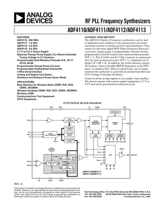
  • 1. a RF PLL Frequency Synthesizers ADF4110/ADF4111/ADF4112/ADF4113 FEATURES GENERAL DESCRIPTION ADF4110: 550 MHz The ADF4110 family of frequency synthesizers can be used ADF4111: 1.2 GHz to implement local oscillators in the upconversion and down- ADF4112: 3.0 GHz conversion sections of wireless receivers and transmitters. They ADF4113: 4.0 GHz consist of a low-noise digital PFD (Phase Frequency Detector), 2.7 V to 5.5 V Power Supply a precision charge pump, a programmable reference divider, Separate Charge Pump Supply (VP) Allows Extended programmable A and B counters and a dual-modulus prescaler Tuning Voltage in 3 V Systems (P/P + 1). The A (6-bit) and B (13-bit) counters, in conjunction Programmable Dual Modulus Prescaler 8/9, 16/17, with the dual modulus prescaler (P/P + 1), implement an N 32/33, 64/65 divider (N = BP + A). In addition, the 14-bit reference counter Programmable Charge Pump Currents (R Counter), allows selectable REFIN frequencies at the PFD Programmable Antibacklash Pulsewidth input. A complete PLL (Phase-Locked Loop) can be imple- 3-Wire Serial Interface mented if the synthesizer is used with an external loop filter and Analog and Digital Lock Detect VCO (Voltage Controlled Oscillator). Hardware and Software Power-Down Mode Control of all the on-chip registers is via a simple 3-wire interface. APPLICATIONS The devices operate with a power supply ranging from 2.7 V to Base Stations for Wireless Radio (GSM, PCS, DCS, 5.5 V and can be powered down when not in use. CDMA, WCDMA) Wireless Handsets (GSM, PCS, DCS, CDMA, WCDMA) Wireless LANS Communications Test Equipment CATV Equipment FUNCTIONAL BLOCK DIAGRAM AVDD DVDD VP CPGND RSET REFERENCE 14-BIT REFIN R COUNTER PHASE FREQUENCY CHARGE DETECTOR PUMP CP 14 R COUNTER LATCH CLK 24-BIT FUNCTION DATA INPUT REGISTER LATCH LOCK CURRENT CURRENT 22 LE DETECT SETTING 1 SETTING 2 A, B COUNTER SDOUT LATCH CPI3 CPI2 CPI1 CPI6 CPI5 CPI4 19 FROM HIGH Z FUNCTION LATCH AVDD 13 MUX MUXOUT N = BP + A 13-BIT B COUNTER SDOUT RFINA LOAD PRESCALER P/P +1 LOAD RFINB 6-BIT A COUNTER M3 M2 M1 ADF4110/ADF4111 6 ADF4112/ADF4113 CE AGND DGND REV. A Information furnished by Analog Devices is believed to be accurate and reliable. However, no responsibility is assumed by Analog Devices for its use, nor for any infringements of patents or other rights of third parties One Technology Way, P.O. Box 9106, Norwood, MA 02062-9106, U.S.A. which may result from its use. No license is granted by implication or Tel: 781/329-4700 World Wide Web Site: http://www.analog.com otherwise under any patent or patent rights of Analog Devices. Fax: 781/326-8703 © Analog Devices, Inc., 2001
  • 2. ADF4110/ADF4111/ADF4112/ADF4113–SPECIFICATIONS1T = T (AV = DV = 3 V 10%, 5 V 10%; AV ≤ V ≤ 6.0 V; AGND = DGND = CPGND = 0 V; R = 4.7 k ; dBm referred to 50 ; DD DD DD P SET A MIN to TMAX unless otherwise noted.) Parameter B Version B Chips2 Unit Test Conditions/Comments RF CHARACTERISTICS (3 V) See Figure 3 for Input Circuit. RF Input Frequency Use a square wave for lower frequencies, ADF4110 80/550 80/550 MHz min/max below the minimum level stated. ADF4110 50/550 50/550 MHz min/max Input Level = –10 dBm ADF4111 0.08/1.2 0.08/1.2 GHz min/max ADF4112 0.2/3.0 0.2/3.0 GHz min/max ADF4112 0.1/3.0 0.1/3.0 GHz min/max Input Level = –10 dBm ADF4113 0.2/3.7 0.2/3.7 GHz min/max Input Level = –10 dBm RF Input Sensitivity –15/0 –15/0 dBm min/max Maximum Allowable Prescaler Output Frequency3 165 165 MHz max RF CHARACTERISTICS (5 V) RF Input Frequency Use a square wave for lower frequencies, ADF4110 80/550 80/550 MHz min/max below the minimum level stated. ADF4111 0.08/1.4 0.08/1.4 GHz min/max ADF4112 0.1/3.0 0.1/3.0 GHz min/max ADF4113 0.2/3.7 0.2/3.7 GHz min/max ADF4113 0.2/4.0 0.2/4.0 GHz min/max Input Level = –5 dBm RF Input Sensitivity –10/0 –10/0 dBm min/max Maximum Allowable Prescaler Output Frequency3 200 200 MHz max REFIN CHARACTERISTICS REFIN Input Frequency 5/100 5/100 MHz min/max For f < 5 MHz, use dc-coupled square wave, (0 to VDD). Reference Input Sensitivity4 –5 –5 dBm min AC-Coupled. When DC-Coupled: 0 to VDD max (CMOS-Compatible) REFIN Input Capacitance 10 10 pF max REFIN Input Current ± 100 ± 100 µA max PHASE DETECTOR Phase Detector Frequency5 55 55 MHz max CHARGE PUMP ICP Sink/Source Programmable: See Table V High Value 5 5 mA typ With RSET = 4.7 kΩ Low Value 625 625 µA typ Absolute Accuracy 2.5 2.5 % typ With RSET = 4.7 kΩ RSET Range 2.7/10 2.7/10 kΩ typ See Table V ICP 3-State Leakage Current 1 1 nA typ Sink and Source Current Matching 2 2 % typ 0.5 V ≤ VCP ≤ VP – 0.5 ICP vs. VCP 1.5 1.5 % typ 0.5 V ≤ VCP ≤ VP – 0.5 ICP vs. Temperature 2 2 % typ VCP = VP/2 LOGIC INPUTS VINH, Input High Voltage 0.8 × DVDD 0.8 × DVDD V min VINL, Input Low Voltage 0.2 × DVDD 0.2 × DVDD V max IINH/IINL, Input Current ±1 ±1 µA max CIN, Input Capacitance 10 10 pF max LOGIC OUTPUTS VOH, Output High Voltage DVDD – 0.4 DVDD – 0.4 V min IOH = 500 µA VOL, Output Low Voltage 0.4 0.4 V max IOL = 500 µA POWER SUPPLIES AVDD 2.7/5.5 2.7/5.5 V min/V max DVDD AVDD AVDD VP AVDD/6.0 AVDD/6.0 V min/V max AVDD ≤ VP ≤ 6.0 V IDD6 (AIDD + DIDD ) See TPCs 21a and 21b ADF4110 5.5 4.5 mA max 4.5 mA Typical ADF4111 5.5 4.5 mA max 4.5 mA Typical ADF4112 7.5 6.5 mA max 6.5 mA Typical ADF4113 11 8.5 mA max 8.5 mA Typical IP 0.5 0.5 mA max TA = 25°C Low Power Sleep Mode 1 1 µA typ –2– REV. A
  • 3. ADF4110/ADF4111/ADF4112/ADF4113 Parameter B Version B Chips2 Unit Test Conditions/Comments NOISE CHARACTERISTICS ADF4113 Phase Noise Floor 7 –171 –171 dBc/Hz typ @ 25 kHz PFD Frequency –164 –164 dBc/Hz typ @ 200 kHz PFD Frequency Phase Noise Performance8 @ VCO Output ADF4110: 540 MHz Output9 –91 –91 dBc/Hz typ @ 1 kHz Offset and 200 kHz PFD Frequency ADF4111: 900 MHz Output10 –87 –87 dBc/Hz typ @ 1 kHz Offset and 200 kHz PFD Frequency ADF4112: 900 MHz Output10 –90 –90 dBc/Hz typ @ 1 kHz Offset and 200 kHz PFD Frequency ADF4113: 900 MHz Output10 –91 –91 dBc/Hz typ @ 1 kHz Offset and 200 kHz PFD Frequency ADF4111: 836 MHz Output11 –78 –78 dBc/Hz typ @ 300 Hz Offset and 30 kHz PFD Frequency ADF4112: 1750 MHz Output 12 –86 –86 dBc/Hz typ @ 1 kHz Offset and 200 kHz PFD Frequency ADF4112: 1750 MHz Output 13 –66 –66 dBc/Hz typ @ 200 Hz Offset and 10 kHz PFD Frequency ADF4112: 1960 MHz Output 14 –84 –84 dBc/Hz typ @ 1 kHz Offset and 200 kHz PFD Frequency ADF4113: 1960 MHz Output 14 –85 –85 dBc/Hz typ @ 1 kHz Offset and 200 kHz PFD Frequency ADF4113: 3100 MHz Output 15 –86 –86 dBc/Hz typ @ 1 kHz Offset and 1 MHz PFD Frequency Spurious Signals ADF4110: 540 MHz Output9 –97/–106 –97/–106 dBc typ @ 200 kHz/400 kHz and 200 kHz PFD Frequency ADF4111: 900 MHz Output10 –98/–110 –98/–110 dBc typ @ 200 kHz/400 kHz and 200 kHz PFD Frequency ADF4112: 900 MHz Output10 –91/–100 –91/–100 dBc typ @ 200 kHz/400 kHz and 200 kHz PFD Frequency ADF4113: 900 MHz Output10 –100/–110 –100/–110 dBc typ @ 200 kHz/400 kHz and 200 kHz PFD Frequency ADF4111: 836 MHz Output11 –81/–84 –81/–84 dBc typ @ 30 kHz/60 kHz and 30 kHz PFD Frequency ADF4112: 1750 MHz Output 12 –88/–90 –88/–90 dBc typ @ 200 kHz/400 kHz and 200 kHz PFD Frequency ADF4112: 1750 MHz Output 13 –65/–73 –65/–73 dBc typ @ 10 kHz/20 kHz and 10 kHz PFD Frequency ADF4112: 1960 MHz Output 14 –80/–84 –80/–84 dBc typ @ 200 kHz/400 kHz and 200 kHz PFD Frequency ADF4113: 1960 MHz Output 14 –80/–84 –80/–84 dBc typ @ 200 kHz/400 kHz and 200 kHz PFD Frequency ADF4113: 3100 MHz Output15 –80/–82 –82/–82 dBc typ @ 1 MHz/2 MHz and 1 MHz PFD Frequency NOTES 1 Operating temperature range is as follows: B Version: –40°C to +85°C. 2 The B Chip specifications are given as typical values. 3 This is the maximum operating frequency of the CMOS counters. The prescaler value should be chosen to ensure that the RF input is divided down to a frequency which is less than this value. 4 AVDD = DVDD = 3 V; For AVDD = DVDD = 5 V, use CMOS-compatible levels. 5 Guaranteed by design. 6 TA = 25°C; AVDD = DVDD = 3 V; P = 16; SYNC = 0; DLY = 0; RFIN for ADF4110 = 540 MHz; RFIN for ADF4111, ADF4112, ADF4113 = 900 MHz. 7 The synthesizer phase noise floor is estimated by measuring the in-band phase noise at the output of the VCO and subtracting 20 logN (where N is the N divider value). 8 The phase noise is measured with the EVAL-ADF411XEB1 Evaluation Board and the HP8562E Spectrum Analyzer. The spectrum analyzer provides the REFIN for the synthesizer (fREFOUT = 10 MHz @ 0 dBm). SYNC = 0; DLY = 0 (See Table III). 9 fREFIN = 10 MHz; fPFD = 200 kHz; Offset frequency = 1 kHz; fRF = 540 MHz; N = 2700; Loop B/W = 20 kHz. 10 fREFIN = 10 MHz; fPFD = 200 kHz; Offset frequency = 1 kHz; fRF = 900 MHz; N = 4500; Loop B/W = 20 kHz. 11 fREFIN = 10 MHz; fPFD = 30 kHz; Offset frequency = 300 Hz; fRF = 836 MHz; N = 27867; Loop B/W = 3 kHz. 12 fREFIN = 10 MHz; fPFD = 200 kHz; Offset frequency = 1 kHz; fRF = 1750 MHz; N = 8750; Loop B/W = 20 kHz. 13 fREFIN = 10 MHz; fPFD = 10 kHz; Offset frequency = 200 Hz; fRF = 1750 MHz; N = 175000; Loop B/W = 1 kHz. 14 fREFIN = 10 MHz; fPFD = 200 kHz; Offset frequency = 1 kHz; fRF = 1960 MHz; N = 9800; Loop B/W = 20 kHz. 15 fREFIN = 10 MHz; fPFD = 1 MHz; Offset frequency = 1 kHz; fRF = 3100 MHz; N = 3100; Loop B/W = 20 kHz. Specifications subject to change without notice. (AVDD = DVDD = 3 V 10%, 5 V 10%; AVDD ≤ VP ≤ 6.0 V; AGND = DGND = CPGND = 0 V; TIMING CHARACTERISTICS1 R SET = 4.7 k ; TA = TMIN to TMAX unless otherwise noted.) Limit at TMIN to TMAX Parameter (B Version) Unit Test Conditions/Comments t1 10 ns min DATA to CLOCK Setup Time t2 10 ns min DATA to CLOCK Hold Time t3 25 ns min CLOCK High Duration t4 25 ns min CLOCK Low Duration t5 10 ns min CLOCK to LE Setup Time t6 20 ns min LE Pulsewidth NOTES 1 Guaranteed by design but not production tested. Specifications subject to change without notice. REV. A –3–
  • 4. ADF4110/ADF4111/ADF4112/ADF4113 t3 t4 CLOCK t1 t2 DB1 DB0 (LSB) DATA DB20 (MSB) DB19 DB2 (CONTROL BIT C2) (CONTROL BIT C1) t6 LE t5 LE Figure 1. Timing Diagram ABSOLUTE MAXIMUM RATINGS 1, 2 CSP θJA Thermal Impedance (Paddle Soldered) . . . 122°C/W (TA = 25°C unless otherwise noted) CSP θJA Thermal Impedance AVDD to GND3 . . . . . . . . . . . . . . . . . . . . . . . . –0.3 V to +7 V (Paddle Not Soldered) . . . . . . . . . . . . . . . . . . . . . 216°C/W AVDD to DVDD . . . . . . . . . . . . . . . . . . . . . . –0.3 V to +0.3 V Lead Temperature, Soldering VP to GND . . . . . . . . . . . . . . . . . . . . . . . . . . . –0.3 V to +7 V Vapor Phase (60 sec) . . . . . . . . . . . . . . . . . . . . . . . . 215°C VP to AVDD . . . . . . . . . . . . . . . . . . . . . . . . . –0.3 V to +5.5 V Infrared (15 sec) . . . . . . . . . . . . . . . . . . . . . . . . . . . . 220°C Digital I/O Voltage to GND . . . . . . . . –0.3 V to VDD + 0.3 V NOTES 1 Analog I/O Voltage to GND . . . . . . . . . –0.3 V to VP + 0.3 V Stresses above those listed under Absolute Maximum Ratings may cause perma- REFIN, RFINA, RFINB to GND . . . . . . –0.3 V to VDD + 0.3 V nent damage to the device. This is a stress rating only; functional operation of the device at these or any other conditions above those listed in the operational RFINA to RFINB . . . . . . . . . . . . . . . . . . . . . . . . . . . ± 320 mV sections of this specification is not implied. Exposure to absolute maximum rating Operating Temperature Range conditions for extended periods may affect device reliability. 2 Industrial (B Version) . . . . . . . . . . . . . . . –40°C to +85°C This device is a high-performance RF integrated circuit with an ESD rating of Storage Temperature Range . . . . . . . . . . . . –65°C to +150°C < 2 kV and it is ESD sensitive. Proper precautions should be taken for handling and assembly. Maximum Junction Temperature . . . . . . . . . . . . . . . . 150°C 3 GND = AGND = DGND = 0 V. TSSOP θJA Thermal Impedance . . . . . . . . . . . . . 150.4°C/W TRANSISTOR COUNT 6425 (CMOS) and 303 (Bipolar). CAUTION ESD (electrostatic discharge) sensitive device. Electrostatic charges as high as 4000 V readily accumu- late on the human body and test equipment and can discharge without detection. Although the WARNING! ADF4110/ADF4111/ADF4112/ADF4113 features proprietary ESD protection circuitry, permanent damage may occur on devices subjected to high-energy electrostatic discharges. Therefore, proper ESD ESD SENSITIVE DEVICE precautions are recommended to avoid performance degradation or loss of functionality. ORDERING GUIDE Model Temperature Range Package Description Package Option* ADF4110BRU –40°C to +85°C Thin Shrink Small Outline Package (TSSOP) RU-16 ADF4110BCP –40°C to +85°C Chip Scale Package (CSP) CP-20 ADF4111BRU –40°C to +85°C Thin Shrink Small Outline Package (TSSOP) RU-16 ADF4111BCP –40°C to +85°C Chip Scale Package (CSP) CP-20 ADF4112BRU –40°C to +85°C Thin Shrink Small Outline Package (TSSOP) RU-16 ADF4112BCP –40°C to +85°C Chip Scale Package (CSP) CP-20 ADF4113BRU –40°C to +85°C Thin Shrink Small Outline Package (TSSOP) RU-16 ADF4113BCP –40°C to +85°C Chip Scale Package (CSP) CP-20 ADF4113BCHIPS –40°C to +85°C DICE DICE *Contact the factory for chip availability. –4– REV. A
  • 5. ADF4110/ADF4111/ADF4112/ADF4113 PIN FUNCTION DESCRIPTIONS Pin No. Mnemonic Function 1 RSET Connecting a resistor between this pin and CPGND sets the maximum charge pump output current. The nominal voltage potential at the RSET pin is 0.56 V. The relationship between ICP and RSET is 23.5 ICP max = RSET So, with RSET = 4.7 kΩ, ICPmax = 5 mA. 2 CP Charge Pump Output. When enabled this provides ±ICP to the external loop filter, which in turn drives the external VCO. 3 CPGND Charge Pump Ground. This is the ground return path for the charge pump. 4 AGND Analog Ground. This is the ground return path of the prescaler. 5 RFINB Complementary Input to the RF Prescaler. This point should be decoupled to the ground plane with a small bypass capacitor, typically 100 pF. See Figure 3. 6 RFINA Input to the RF Prescaler. This small signal input is ac-coupled from the VCO. 7 AVDD Analog Power Supply. This may range from 2.7 V to 5.5 V. Decoupling capacitors to the analog ground plane should be placed as close as possible to this pin. AVDD must be the same value as DVDD. 8 REFIN Reference Input. This is a CMOS input with a nominal threshold of VDD/2 and an equivalent input resis- tance of 100 kΩ. See Figure 2. This input can be driven from a TTL or CMOS crystal oscillator or it can be ac-coupled. 9 DGND Digital Ground. 10 CE Chip Enable. A logic low on this pin powers down the device and puts the charge pump output into three- state mode. Taking the pin high will power up the device depending on the status of the power-down bit F2. 11 CLK Serial Clock Input. This serial clock is used to clock in the serial data to the registers. The data is latched into the 24-bit shift register on the CLK rising edge. This input is a high impedance CMOS input. 12 DATA Serial Data Input. The serial data is loaded MSB first with the two LSBs being the control bits. This input is a high impedance CMOS input. 13 LE Load Enable, CMOS Input. When LE goes high, the data stored in the shift registers is loaded into one of the four latches, the latch being selected using the control bits. 14 MUXOUT This multiplexer output allows either the Lock Detect, the scaled RF or the scaled Reference Frequency to be accessed externally. 15 DVDD Digital Power Supply. This may range from 2.7 V to 5.5 V. Decoupling capacitors to the digital ground plane should be placed as close as possible to this pin. DVDD must be the same value as AVDD. 16 VP Charge Pump Power Supply. This should be greater than or equal to VDD. In systems where VDD is 3 V, it can be set to 6 V and used to drive a VCO with a tuning range of up to 6 V. PIN CONFIGURATIONS TSSOP CHIP SCALE PACKAGE 17 DVDD 16 DVDD 19 RSET RSET 1 16 VP 20 CP 18 VP CP 2 15 DVDD ADF4110 CPGND 3 ADF4111 14 MUXOUT CPGND 1 15 MUXOUT ADF4112 ADF4110 AGND 4 ADF4113 13 LE AGND 2 ADF4111 14 LE TOP VIEW 12 DATA ADF4112 RFINB 5 AGND 3 13 DATA (Not to Scale) ADF4113 RFINA 6 11 CLK RFINB 4 TOP VIEW 12 CLK (Not to Scale) AVDD 7 10 CE RFINA 5 11 CE REFIN 8 9 DGND DGND 10 AVDD 6 AVDD 7 REFIN 8 DGND 9 REV. A –5–
  • 6. ADF4110/ADF4111/ADF4112/ADF4113 0 FREQ-UNIT PARAM-TYPE DATA-FORMAT KEYWORD IMPEDANCE – OHMS REFERENCE VDD = 3V, VP = 5V GHz S MA R 50 –10 LEVEL = –4.2dBm ICP = 5mA FREQ MAGS11 ANGS11 FREQ MAGS11 ANGS11 –20 PFD FREQUENCY = 200kHz 0.05 0.89207 –2.0571 1.05 0.9512 –40.134 LOOP BANDWIDTH = 20kHz 0.10 0.8886 –4.4427 1.10 0.93458 –43.747 OUTPUT POWER – dB 0.15 0.89022 –6.3212 1.15 0.94782 –44.393 –30 RES. BANDWIDTH = 10Hz 0.20 0.96323 –2.1393 1.20 0.96875 –46.937 VIDEO BANDWIDTH = 10Hz 0.25 0.90566 –12.13 1.25 0.92216 –49.6 SWEEP = 1.9 SECONDS 0.30 0.90307 –13.52 1.30 0.93755 –51.884 –40 0.35 0.89318 –15.746 1.35 0.96178 –51.21 AVERAGES = 19 0.40 0.89806 –18.056 1.40 0.94354 –53.55 –50 0.45 0.89565 –19.693 1.45 0.95189 –56.786 0.50 0.88538 –22.246 1.50 0.97647 –58.781 0.55 0.89699 –24.336 1.55 0.98619 –60.545 –60 0.60 0.89927 –25.948 1.60 0.95459 –61.43 0.65 0.87797 –28.457 1.65 0.97945 –61.241 0.70 0.90765 –29.735 1.70 0.98864 –64.051 –70 –92.5dBc/Hz 0.75 0.88526 –31.879 1.75 0.97399 –66.19 0.80 0.81267 –32.681 1.80 0.97216 –63.775 0.85 0.90357 –31.522 –80 0.90 0.92954 –34.222 0.95 0.92087 –36.961 –90 1.00 0.93788 –39.343 –100 –2kHz –1kHz 900MHz +1kHz +2kHz TPC 1. S-Parameter Data for the ADF4113 RF Input (Up TPC 4. ADF4113 Phase Noise (900 MHz, 200 kHz, to 1.8 GHz) 20 kHz) with DLY and SYNC Enabled 10dB/DIVISION RL = –40dBc/Hz RMS NOISE = 0.52 0 –40 VDD = 3V –50 –5 VP = 3V –60 0.52 rms RF INPUT POWER – dBm –10 PHASE NOISE – dBc/Hz –70 –80 –15 –90 –20 TA = +85 C –100 TA = +25 C –25 –110 –120 –30 –130 TA = –40 C –35 –140 0 1 2 3 4 5 100Hz FREQUENCY OFFSET FROM 900MHz CARRIER 1MHz RF INPUT FREQUENCY – GHz TPC 2. Input Sensitivity (ADF4113) TPC 5. ADF4113 Integrated Phase Noise (900 MHz, 200 kHz, 20 kHz, Typical Lock Time: 400 µ s) 10dB/DIVISION RL = –40dBc/Hz RMS NOISE = 0.62 0 –40 REFERENCE VDD = 3V, VP = 5V –10 –50 LEVEL = –4.2dBm ICP = 5mA –20 PFD FREQUENCY = 200kHz –60 LOOP BANDWIDTH = 20kHz 0.62 rms PHASE NOISE – dBc/Hz OUTPUT POWER – dB –30 RES. BANDWIDTH = 10Hz –70 VIDEO BANDWIDTH = 10Hz –40 SWEEP = 1.9 SECONDS –80 AVERAGES = 19 –50 –90 –60 –100 –70 –91.0dBc/Hz –110 –80 –120 –90 –130 –100 –140 –2kHz –1kHz 900MHz +1kHz +2kHz 100Hz FREQUENCY OFFSET FROM 900MHz CARRIER 1MHz TPC 3. ADF4113 Phase Noise (900 MHz, 200 kHz, 20 kHz) TPC 6. ADF4113 Integrated Phase Noise (900 MHz, 200 kHz, 35 kHz, Typical Lock Time: 200 µ s) –6– REV. A
  • 7. ADF4110/ADF4111/ADF4112/ADF4113 10dB/DIVISION RL = –40dBc/Hz RMS NOISE = 1.6 0 –40 REFERENCE VDD = 3V, VP = 5V –10 LEVEL = –4.2dBm –50 ICP = 5mA –20 PFD FREQUENCY = 200kHz –60 LOOP BANDWIDTH = 20kHz PHASE NOISE – dBc/Hz RES. BANDWIDTH = 1kHz –70 OUTPUT POWER – dB –30 VIDEO BANDWIDTH = 1kHz 1.6 rms –40 SWEEP = 2.5 SECONDS –80 AVERAGES = 30 –50 –90 –60 –100 –70 –110 –80 –90.2dBc –120 –90 –130 –100 –140 –400kHz –200kHz 900MHz +200kHz +400kHz 100Hz FREQUENCY OFFSET FROM 1750MHz CARRIER 1MHz TPC 7. ADF4113 Reference Spurs (900 MHz, 200 kHz, TPC 10. ADF4113 Integrated Phase Noise (1750 MHz, 20 kHz) 30 kHz, 3 kHz) 0 0 VDD = 3V, VP = 5V REFERENCE VDD = 3V, VP = 5V REFERENCE –10 LEVEL = –4.2dBm –10 LEVEL = –5.7dBm ICP = 5mA ICP = 5mA PFD FREQUENCY = 30kHz PFD FREQUENCY = 200kHz –20 –20 LOOP BANDWIDTH = 3kHz LOOP BANDWIDTH = 35kHz RES. BANDWIDTH = 3Hz RES. BANDWIDTH = 1kHz POWER OUTPUT – dB –30 OUTPUT POWER – dB –30 VIDEO BANDWIDTH = 3Hz VIDEO BANDWIDTH = 1kHz SWEEP = 255 SECONDS –40 SWEEP = 2.5 SECONDS –40 POSITIVE PEAK DETECT AVERAGES = 30 MODE –50 –50 –60 –60 –70 –70 –79.6dBc –80 –89.3dBc –80 –90 –90 –100 –100 –400kHz –200kHz 900MHz +200kHz +400kHz –80kHz –40kHz 1750MHz +40kHz +80kHz TPC 8. ADF4113 Reference Spurs (900 MHz, 200 kHz, TPC 11. ADF4113 Reference Spurs (1750 MHz, 30 kHz, 35 kHz) 3 kHz) 0 0 REFERENCE VDD = 3V, VP = 5V REFERENCE VDD = 3V, VP = 5V –10 LEVEL = –8.0dBm ICP = 5mA –10 LEVEL = –4.2dBm ICP = 5mA PFD FREQUENCY = 30kHz PFD FREQUENCY = 1MHz –20 –20 LOOP BANDWIDTH = 100kHz LOOP BANDWIDTH = 3kHz RES. BANDWIDTH = 10kHz RES. BANDWIDTH = 10Hz OUTPUT POWER – dB –30 OUTPUT POWER – dB –30 VIDEO BANDWIDTH = 10kHz VIDEO BANDWIDTH = 10Hz SWEEP = 477ms SWEEP = 1.9 SECONDS –40 –40 AVERAGES = 10 AVERAGES = 45 –50 –50 –60 –60 –86.6dBc/Hz –70 –70 –80 –75.2dBc/Hz –80 –90 –90 –100 –100 –400Hz –200Hz 1750MHz +200Hz +400Hz –2kHz –1kHz 3100MHz +1kHz +2kHz TPC 9. ADF4113 Phase Noise (1750 MHz, 30 kHz, 3 kHz) TPC 12. ADF4113 Phase Noise (3100 MHz, 1 MHz, 100 kHz) REV. A –7–
  • 8. ADF4110/ADF4111/ADF4112/ADF4113 10dB/DIVISION RL = –40dBc/Hz RMS NOISE = 1.7 –60 –40 –50 VDD = 3V VP = 3V –60 1.7 rms –70 PHASE NOISE – dBc/Hz PHASE NOISE – dBc/Hz –70 –80 –80 –90 –100 –110 –90 –120 –130 –100 –140 –40 –20 0 20 40 60 80 100 100Hz FREQUENCY OFFSET FROM 3100MHz CARRIER 1MHz TEMPERATURE – C TPC 13. ADF4113 Integrated Phase Noise (3100 MHz, TPC 16. ADF4113 Phase Noise vs. Temperature 1 MHz, 100 kHz) (900 MHz, 200 kHz, 20 kHz) 0 –60 REFERENCE VDD = 3V, VP = 5V –10 LEVEL = –17.2dBm ICP = 5mA VDD = 3V PFD FREQUENCY = 1MHz VP = 5V FIRST REFERENCE SPUR – dBc –20 LOOP BANDWIDTH = 100kHz –70 OUTPUT POWER – dB –30 RES. BANDWIDTH = 1kHz VIDEO BANDWIDTH = 1kHz –40 SWEEP = 13 SECONDS AVERAGES = 1 –50 –80 –60 –70 –80.6dBc –90 –80 –90 –100 –100 –2MHz –1MHz 3100MHz +1MHz +2MHz –40 –20 0 20 40 60 80 100 TEMPERATURE – C TPC 14. ADF4113 Reference Spurs (3100 MHz, 1 MHz, TPC 17. ADF4113 Reference Spurs vs. Temperature 100 kHz) (900 MHz, 200 kHz, 20 kHz) –120 –5 VDD = 3V VP = 5V –15 VDD = 3V –130 VP = 5V FIRST REFERENCE SPUR – dBc –25 PHASE NOISE – dBc/Hz –140 –35 –45 –150 –55 –65 –160 –75 –170 –85 –95 –180 –105 1 10 100 1000 10000 0 1 2 3 4 5 PHASE DETECTOR FREQUENCY – kHz TUNING VOLTAGE – Volts TPC 15. ADF4113 Phase Noise (Referred to CP Output) TPC 18. ADF4113 Reference Spurs (200 kHz) vs. VTUNE vs. PFD Frequency (900 MHz, 200 kHz, 20 kHz) –8– REV. A
  • 9. ADF4110/ADF4111/ADF4112/ADF4113 –60 10 VDD = 3V 9 VP = 5V 8 ADF4113 –70 PHASE NOISE – dBc/Hz 7 6 AIDD – mA –80 5 ADF4112 4 3 –90 2 ADF4110 1 ADF4111 –100 0 –40 –20 0 20 40 60 80 100 0 8/9 16/17 32/33 64/65 TEMPERATURE – C PRESCALER VALUE TPC 19. ADF4113 Phase Noise vs. Temperature TPC 21a. AIDD vs. Prescaler Value (836 MHz, 30 kHz, 3 kHz) –60 3.0 VDD = 3V VDD = 3V VP = 3V VP = 5V 2.5 FIRST REFERENCE SPUR – dBc –70 DIDD – mA 2.0 –80 1.5 1.0 –90 0.5 –100 0 –40 –20 0 20 40 60 80 100 0 50 100 150 200 TEMPERATURE – C PRESCALER OUTPUT FREQUENCY – MHz TPC 20. ADF4113 Reference Spurs vs. Temperature TPC 21b. DIDD vs. Prescaler Output Frequency (836 MHz, 30 kHz, 3 kHz) (ADF4110, ADF4111, ADF4112, ADF4113) 6 5 4 VPP = 5V 3 ICP SETTING : 5mA 2 1 lCP – mA 0 –1 –2 –3 –4 –5 –6 0 0.5 1 1.5 2 2.5 3 3.5 4 4.5 5 VCP – Volts TPC 22. Charge Pump Output Characteristics for ADF4110 Family REV. A –9–
  • 10. ADF4110/ADF4111/ADF4112/ADF4113 CIRCUIT DESCRIPTION Pulse Swallow Function REFERENCE INPUT SECTION The A and B counters, in conjunction with the dual modulus The reference input stage is shown in Figure 2. SW1 and SW2 prescaler, make it possible to generate output frequencies that are normally-closed switches. SW3 is normally-open. When are spaced only by the Reference Frequency divided by R. The power-down is initiated, SW3 is closed and SW1 and SW2 are equation for the VCO frequency is as follows: opened. This ensures that there is no loading of the REFIN pin fVCO = [(P × B) + A] × fREFIN/R on power-down. fVCO Output frequency of external voltage controlled oscilla- POWER-DOWN tor (VCO). CONTROL P Preset modulus of dual modulus prescaler NC 100k B Preset Divide Ratio of binary 13-bit counter (3 to 8191). SW2 REFIN NC TO R COUNTER A Preset Divide Ratio of binary 6-bit swallow counter (0 to BUFFER 63). SW1 SW3 NO fREFIN Output frequency of the external reference frequency oscillator. Figure 2. Reference Input Stage R Preset divide ratio of binary 14-bit programmable refer- ence counter (1 to 16383). RF INPUT STAGE The RF input stage is shown in Figure 3. It is followed by a R COUNTER 2-stage limiting amplifier to generate the CML (Current Mode The 14-bit R counter allows the input reference frequency to be Logic) clock levels needed for the prescaler. divided down to produce the reference clock to the phase fre- quency detector (PFD). Division ratios from 1 to 16,383 are allowed. BIAS 1.6V GENERATOR AVDD 500 500 N = BP + A 13-BIT B TO PFD RFINA COUNTER FROM RF INPUT STAGE LOAD PRESCALER RFINB P/P + 1 LOAD MODULUS 6-BIT A CONTROL COUNTER AGND Figure 3. RF Input Stage Figure 4. A and B Counters PRESCALER (P/P+1) The dual-modulus prescaler (P/P+1), along with the A and B PHASE FREQUENCY DETECTOR (PFD) AND CHARGE counters, enables the large division ratio, N, to be realized PUMP (N = BP + A). The dual-modulus prescaler, operating at CML The PFD takes inputs from the R counter and N counter levels, takes the clock from the RF input stage and divides it (N = BP + A) and produces an output proportional to the phase down to a manageable frequency for the CMOS A and B counters. and frequency difference between them. Figure 5 is a simplified The prescaler is programmable. It can be set in software to 8/9, schematic. The PFD includes a programmable delay element 16/17, 32/33, or 64/65. It is based on a synchronous 4/5 core. which controls the width of the antibacklash pulse. This pulse ensures that there is no dead zone in the PFD transfer function A AND B COUNTERS and minimizes phase noise and reference spurs. Two bits in the The A and B CMOS counters combine with the dual modulus Reference Counter Latch, ABP2 and ABP1 control the width prescaler to allow a wide ranging division ratio in the PLL feed- of the pulse. See Table III. back counter. The counters are specified to work when the prescaler output is 200 MHz or less. Thus, with an RF input frequency of 2.5 GHz, a prescaler value of 16/17 is valid but a value of 8/9 is not valid. –10– REV. A
  • 11. ADF4110/ADF4111/ADF4112/ADF4113 VP The N-channel open-drain analog lock detect should be oper- CHARGE PUMP ated with an external pull-up resistor of 10 kΩ nominal. When UP lock has been detected this output will be high with narrow low- HI D1 Q1 going pulses. U1 DVDD R DIVIDER CLR1 PROGRAMMABLE CP ANALOG LOCK DETECT U3 DELAY DIGITAL LOCK DETECT R COUNTER OUTPUT MUX CONTROL MUXOUT N COUNTER OUTPUT ABP1 ABP2 SDOUT CLR2 DOWN HI D2 Q2 U2 DGND N DIVIDER Figure 6. MUXOUT Circuit CPGND INPUT SHIFT REGISTER The ADF4110 family digital section includes a 24-bit input shift R DIVIDER register, a 14-bit R counter and a 19-bit N counter, comprising a 6-bit A counter and a 13-bit B counter. Data is clocked into N DIVIDER the 24-bit shift register on each rising edge of CLK. The data is clocked in MSB first. Data is transferred from the shift register CP OUTPUT to one of four latches on the rising edge of LE. The destination latch is determined by the state of the two control bits (C2, C1) in the shift register. These are the two LSBs DB1, DB0 as Figure 5. PFD Simplified Schematic and Timing shown in the timing diagram of Figure 1. The truth table for (In Lock) these bits is shown in Table VI. Table I shows a summary of how the latches are programmed. MUXOUT AND LOCK DETECT The output multiplexer on the ADF4110 family allows the Table I. C2, C1 Truth Table user to access various internal points on the chip. The state of MUXOUT is controlled by M3, M2 and M1 in the function Control Bits latch. Table V shows the full truth table. Figure 6 shows the C2 C1 Data Latch MUXOUT section in block diagram form. 0 0 R Counter Lock Detect 0 1 N Counter (A and B) MUXOUT can be programmed for two types of lock detect: 1 0 Function Latch (Including Prescaler) digital lock detect and analog lock detect. 1 1 Initialization Latch Digital lock detect is active high. When LDP in the R counter latch is set to 0, digital lock detect is set high when the phase error on three consecutive Phase Detector cycles is less than 15 ns. With LDP set to 1, five consecutive cycles of less than 15 ns are required to set the lock detect. It will stay set high until a phase error of greater than 25 ns is detected on any subsequent PD cycle. REV. A –11–
  • 12. ADF4110/ADF4111/ADF4112/ADF4113 Table II. ADF4110 Family Latch Summary REFERENCE COUNTER LATCH RESERVED PRECISION DETECT LOCK ANTI- TEST BACKLASH CONTROL DLY SYNC MODE BITS WIDTH 14-BIT REFERENCE COUNTER, R BITS DB23 DB22 DB21 DB20 DB19 DB18 DB17 DB16 DB15 DB14 DB13 DB12 DB11 DB10 DB9 DB8 DB7 DB6 DB5 DB4 DB3 DB2 DB1 DB0 X DLY SYNC LDP T2 T1 ABP2 ABP1 R14 R13 R12 R11 R10 R9 R8 R7 R6 R5 R4 R3 R2 R1 C2 (0) C1 (0) X = DON'T CARE N COUNTER LATCH CP GAIN CONTROL RESERVED 13-BIT B COUNTER 6-BIT A COUNTER BITS DB23 DB22 DB21 DB20 DB19 DB18 DB17 DB16 DB15 DB14 DB13 DB12 DB11 DB10 DB9 DB8 DB7 DB6 DB5 DB4 DB3 DB2 DB1 DB0 X X G1 B13 B12 B11 B10 B9 B8 B7 B6 B5 B4 B3 B2 B1 A6 A5 A4 A3 A2 A1 C2 (0) C1 (1) X = DON'T CARE FUNCTION LATCH FASTLOCK FASTLOCK POLARITY COUNTER POWER- ENABLE POWER- DOWN 2 DOWN 1 THREE- RESET STATE MODE CURRENT CURRENT PD CP PRESCALER SETTING SETTING TIMER COUNTER MUXOUT CONTROL VALUE 2 1 CONTROL CONTROL BITS DB23 DB22 DB21 DB20 DB19 DB18 DB17 DB16 DB15 DB14 DB13 DB12 DB11 DB10 DB9 DB8 DB7 DB6 DB5 DB4 DB3 DB2 DB1 DB0 P2 P1 PD2 CPI6 CPI5 CPI4 CPI3 CPI2 CPI1 TC4 TC3 TC2 TC1 F5 F4 F3 F2 M3 M2 M1 PD1 F1 C2 (1) C1 (0) INITIALIZATION LATCH FASTLOCK FASTLOCK COUNTER POLARITY ENABLE POWER- POWER- DOWN 1 DOWN 2 THREE- RESET STATE MODE CURRENT CURRENT CP PD PRESCALER SETTING SETTING TIMER COUNTER MUXOUT CONTROL VALUE 2 1 CONTROL CONTROL BITS DB23 DB22 DB21 DB20 DB19 DB18 DB17 DB16 DB15 DB14 DB13 DB12 DB11 DB10 DB9 DB8 DB7 DB6 DB5 DB4 DB3 DB2 DB1 DB0 P2 P1 PD2 CPI6 CPI5 CPI4 CPI3 CPI2 CPI1 TC4 TC3 TC2 TC1 F5 F4 F3 F2 M3 M2 M1 PD1 F1 C2 (1) C1 (1) –12– REV. A
  • 13. ADF4110/ADF4111/ADF4112/ADF4113 Table III. Reference Counter Latch Map RESERVED PRECISION DETECT LOCK ANTI- TEST BACKLASH CONTROL DLY SYNC MODE BITS WIDTH 14-BIT REFERENCE COUNTER BITS DB23 DB22 DB21 DB20 DB19 DB18 DB17 DB16 DB15 DB14 DB13 DB12 DB11 DB10 DB9 DB8 DB7 DB6 DB5 DB4 DB3 DB2 DB1 DB0 X DLY SYNC LDP T2 T1 ABP2 ABP1 R14 R13 R12 R11 R10 R9 R8 R7 R6 R5 R4 R3 R2 R1 C2 (0) C1 (0) X = DON'T CARE R14 R13 R12 •••••••••• R3 R2 R1 DIVIDE RATIO 0 0 0 •••••••••• 0 0 1 1 0 0 0 •••••••••• 0 1 0 2 0 0 0 •••••••••• 0 1 1 3 0 0 0 •••••••••• 1 0 0 4 • • • •••••••••• • • • • • • • •••••••••• • • • • • • • •••••••••• • • • • 1 1 1 •••••••••• 1 0 0 16380 1 1 1 •••••••••• 1 0 1 16381 1 1 1 •••••••••• 1 1 0 16382 1 1 1 •••••••••• 1 1 1 16383 ABP2 ABP1 ANTIBACKLASH PULSEWIDTH 0 0 3.0ns 0 1 1.5ns 1 0 6.0ns 1 1 3.0ns TEST MODE BITS SHOULD BE SET TO 00 FOR NORMAL OPERATION LDP OPERATION 0 THREE CONSECUTIVE CYCLES OF PHASE DELAY LESS THAN 15ns MUST OCCUR BEFORE LOCK DETECT IS SET. 1 FIVE CONSECUTIVE CYCLES OF PHASE DELAY LESS THAN 15ns MUST OCCUR BEFORE LOCK DETECT IS SET. DLY SYNC OPERATION 0 0 NORMAL OPERATION 0 1 OUTPUT OF PRESCALER IS RESYNCHRONIZED WITH NONDELAYED VERSION OF RF INPUT 1 0 NORMAL OPERATION 1 1 OUTPUT OF PRESCALER IS RESYNCHRONIZED WITH DELAYED VERSION OF RF INPUT REV. A –13–