circuit board repair
•
0 gostou•60 visualizações

The circuit board repair method for repairing damaged circuit traces employs the use of copper circuit tracks which are epoxied to the circuit board. The replaced conductors are the same size as the original.

Recomendados
Mais conteúdo relacionado
Destaque
Destaque (16)
Semelhante a circuit board repair
Semelhante a circuit board repair (20)
Último
Último (20)
circuit board repair
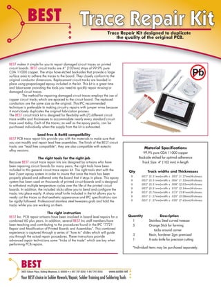
- 1. Trace Repair Kit designed to duplicate the quality of the original PCB. BEST makes it simple for you to repair damaged circuit traces on printed circuit boards. BEST circuit tracks are 4” (102mm) strips of 99.9% pure CDA 11000 copper. The strips have etched backsides that provide a large surface area to adhere the traces to the board. They closely conform to the original conductor dimensions. Replacement circuit tracks are bonded in place using prepackaged epoxy included in the kit. This kit is a great time and labor-saver providing the tools you need to quickly repair missing or damaged circuit traces. The method for repairing damaged circuit traces employs the use of copper circuit tracks which are epoxied to the circuit board. The replaced conductors are the same size as the original. This IPC recommended technique is preferable to making circuitry repairs with jumper wires because it most closely duplicates the original fabrication process. The BEST circuit track kit is designed for flexibility with (7) different circuit trace widths and thicknesses to accommodate nearly every standard circuit trace used today. Each of the traces, as well as the epoxy packs, can be purchased individually when the supply from the kit is exhausted. Lead free & RoHS compatibility BEST PCB trace repair kits provide you with the materials to make sure that you can modify and repair lead free assemblies. The finish of the BEST circuit tracks are “lead free compatible”; they are also compatible with eutectic alloy versions. The right tools for the right job Because BEST circuit trace repair kits are designed by artisans who have been repairing circuit boards for many years, the right tools have been included in this general circuit trace repair kit. The right tools start with the best 2-part epoxy system in order to insure that once the track has been properly placed and adhered onto the board that it stays in place. This epoxy system has been used on thousands of printed circuit boards and is designed to withstand multiple temperature cycles over the life of the printed circuit boards. In addition, the included sticks allow you to bend and configure the tracks into place easily. A sharp small knife included in the kit allows you to neatly cut the traces so that aesthetic appearance and IPC specifications can be rigidly followed. Professional stainless steel tweezers grab and hold the tracks while you are working on them. The right instruction BEST Inc. PCB repair artisans have been involved in board level repairs for a combined 60 plus years. In addition, several BEST Inc staff members have been teaching and contributing to the procedures found in the IPC “7721 Repair and Modification of Printed Boards and Assemblies”. This combined experience is captured through a series of “how to” slides which will guide you through the actual repair procedures. These instructions provide advanced repair technicians some “tricks of the trade” which are key when performing PCB repairs. Material Specifications 99.9% pure CDA 11000 copper Backside etched for optimal adherence Track Size: 4” (102 mm) in length Quantity Description 1 Stainless Steel curved tweezer 5 Orange Stick for forming tacks around corner 3 Resin, hardener 2gm premixed 1 X-acto knife for precision cutting *Individual items may be purchased separately. Qty Track widths and Thicknesses .002” (0.51mm)width x .005” (1.27mm)thickness .002” (0.51mm)width x .006” (1.52mm)thickness .002” (0.51mm)width x .008” (2.03mm)thickness .002” (0.51mm)width x .010” (2.54mm)thickness .003” (0.76mm)width x .015” (3.81mm)thickness .005” (1.27mm)width x .020” (5.08mm)thickness .005” (1.27mm)width x .030” (7.62mm)thickness 9 9 9 9 9 9 9