
Recomendados
Recomendados
Mais conteúdo relacionado
Mais procurados
Mais procurados (20)
Destaque
Destaque (20)
Semelhante a Project overview
Semelhante a Project overview (20)
Project overview
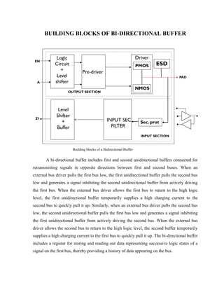
- 1. BUILDING BLOCKS OF BI-DIRECTIONAL BUFFER Building blocks of a Bidirectional Buffer A bi-directional buffer includes first and second unidirectional buffers connected for retransmitting signals in opposite directions between first and second buses. When an external bus driver pulls the first bus low, the first unidirectional buffer pulls the second bus low and generates a signal inhibiting the second unidirectional buffer from actively driving the first bus. When the external bus driver allows the first bus to return to the high logic level, the first unidirectional buffer temporarily supplies a high charging current to the second bus to quickly pull it up. Similarly, when an external bus driver pulls the second bus low, the second unidirectional buffer pulls the first bus low and generates a signal inhibiting the first unidirectional buffer from actively driving the second bus. When the external bus driver allows the second bus to return to the high logic level, the second buffer temporarily supplies a high charging current to the first bus to quickly pull it up. The bi-directional buffer includes a register for storing and reading out data representing successive logic states of a signal on the first bus, thereby providing a history of data appearing on the bus.
- 2. Bidirectional I/O Buffers are preferred because i. Drive different load currents as per specification ii. Minimize noise from the input signal iii. Provide interface between ICs with different signal levels iv. Protect internal circuit from extremely high voltages v. Low to High and High to Low level shifting Above figure shows the block diagram of a Bidirectional I/O cell, comprising of the Input section and the Output section. Each block has been designed to carry out a specific task to reduce the overall design complexity of the I/O device. The bidirectional buffer mainly includes two sections: 1) Output section 2) Input Section OUTPUT SECTION The output section comprises of the following blocks: a) Level Shifter (LOW TO HIGH) with a logic Circuit b) Pre-driver c) Driver d) ESD protection Driver This block is used to drive the current at the PAD. The length and width of the circuit is chosen as per device specifications of the project. Pre-Driver Pre-Driver is the controller block of the output section and it controls the Driver as it guides the Driver about when to drive the current and how much current to drive. There are basically two drivers (4m and 20m drivers). The two Pre-Drivers are connected parallelly.
- 3. Level Shifter The output section needs a transition from low voltage to high voltage. The circuit used for this transition is a CROSS-COUPLED C-MOS. ESD The Electro Static Discharge is a protection layer against the additional environmental generated voltages which could happen due to the human touch or other such conditions. INPUT SECTION The input section comprises of the following blocks: a) Low pass digital filter b) Level Shifter (HIGH TO LOW) with a logic Circuit