This document summarizes Nathan Wendt's final project for EE321, which involved designing third-order passive frequency-selective circuits. Section I derives the general transfer function and analyzes low-pass behavior. Section II examines the low-pass frequency response and Butterworth design. Section III designs a high-pass Butterworth filter. MATLAB is used throughout to simulate and analyze the circuit designs.
2. Wendt 1
INTRODUCTION
This report documents the process and results of designing various passive, third-order,
frequency-selective circuits. All of the circuits designed and analyzed in this report have the
same structure (as seen on the cover or figure1) while the behavior is manipulated by changing
the components and their configuration. Sections I and II focus on a low-pass configuration
while section III covers a high-pass configuration.
SECTION I: General Transfer Function and Low-Pass Behavior
A) S-domain transfer function
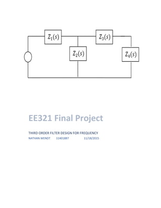
In the frequency domain, the circuit elements can be represented by their
complex impedances. This enables us to use basic circuit analysis techniques to determine the
s-domain transfer function, H(s). To determine the output value, V0(s), in terms of input value,
Vi(s), and complex impedances Z1, Z2, Z3, and Z4 we utilize Kirchhoff’s voltage law around the
loops shown in figure 1.
Figure 1: Complex impedance representation of circuit. Loop 1 on left, loop 2 on right.
KVL loop 1:
𝑉𝑖(𝑠) − 𝑍1 𝐼1 − 𝑍2(𝐼1 − 𝐼2) = 0
KVL loop 2:
𝐼1 𝑍2 − 𝐼2(𝑍2 + 𝑍3 + 𝑍4) = 0
𝐼1 =
𝑍2 + 𝑍3 + 𝑍4
𝑍2
𝐼2
1 2
4. Wendt 3
Also noting:
𝑖2 𝑅 +
1
𝐶4
∫ 𝑖2 𝑑𝑡 = −
1
𝐶2
∫ 𝑖2 𝑑𝑡 +
1
𝐶2
∫ 𝑖1 𝑑𝑡
Substitute the above two equations into KVL 1 and substitute:
1
𝐶4
∫ 𝑖2 𝑑𝑡 = 𝑣0(𝑡)
End up with
𝑣𝑖(𝑡) = 𝐿𝑅𝐶2
𝑑2
𝑖2
𝑑𝑡2
+ (
𝐿𝐶2
𝐶4
+ 𝐿)
𝑑𝑖2
𝑑𝑡
+ 𝑅𝑖2 + 𝑣𝑜(𝑡)
Transfer to the s domain, noting that initial conditions = 0:
𝑉𝑖(𝑠) = 𝐿𝑅𝐶2 𝐼2 𝑠2
+ (
𝐿𝐶2
𝐶4
+ 𝐿) 𝐼2 𝑠 + 𝑅𝐼2 + 𝑉𝑜(𝑠)
Substituting:
𝑉𝑜(𝑠) =
𝐼2
𝑠𝐶4
𝑉𝑖(𝑠) = 𝐿𝑅𝐶2 𝐶4 𝑉𝑜(𝑠)𝑠3
+ (𝐿𝐶2 + 𝐿𝐶4)𝑉𝑜(𝑠)𝑠2
+ 𝑅𝐶4 𝑉𝑜(𝑠)𝑠 + 𝑉𝑜(𝑠)
Translating back to the time domain gives the third order differential equation:
𝑣𝑖(𝑡) = 𝐿𝑅𝐶2 𝐶4
𝑑3
𝑣𝑜(𝑡)
𝑑𝑡3
+ (𝐿𝐶2 + 𝐿𝐶4)
𝑑2
𝑣𝑜(𝑡)
𝑑𝑡2
+ 𝑅𝐶4
𝑑𝑣𝑜(𝑡)
𝑑𝑡
+ 𝑣𝑜(𝑡)
From this equation the state equation matrices are:
𝐴 =
0 1 0
0 0 1
−1
𝐿𝑅𝐶4 𝐶2
−1
𝐿𝐶2
−(𝐶1 + 𝐶2)
(𝑅𝐶1 𝐶2)
𝐵 =
0
0
1
𝐿𝑅𝐶4 𝐶2
𝐶 =
1 0 0
−1 −(𝑅𝐶2) 0
0 0 0
𝐷 =
0
1
0
with 𝑦 =
𝑣𝑜
𝑣 𝐿
5. Wendt 4
Using MATLAB’s lsim function and the state matrices listed above, the step responses of
vo and vL were determined and plotted shown in Figure 2:
Figure 3: Step response of vo and inductor voltage. vo → 1 and vL → 0 as ω → ∞
The lsiminfo function produced data on 100% rise time, peak, and 2% settling time:
Figure 4: Step response data (left) and annotated plot (right)
6. Wendt 5
SECTION II: Low-Pass Frequency Response, Sinusoidal Steady
State, and Butterworth
A) Zeros, Poles, Frequency Response, and Sinusoidal Steady State
The poles and zeros of a function represent the values of s that result in a zero
denominator or numerator respectively. In the case of the low-pass filter, the numerator is a
constant and thus there are no zeros. To find the poles, the denominator must first be factored.
MATLAB was used in this step to factor and determine the poles. Being a third-order filter,
there were 3 poles:
𝑃 =
−639.9
−330.3 + 𝑗3005.9
−330.3 − 𝑗3005.9
One real pole and one complex conjugate pair for a total of three poles. Below is a plot
of the poles on the real vs imaginary plane:
Figure 5: Three poles of third-order low-pass filter
7. Wendt 6
The Bode plot of the transfer function shows the relations between the logarithmic
magnitude of gain and phase with respect to input frequency. Using MATLAB’s bode() function,
the frequency response to of the systems transfer function is plotted shown below:
Figure 6: Bode Diagram for third-order low-pass filter
A frequency of 0 correlates to a DC or unit-step input. Being that the y-axis depicts
20log10|H(jw)|, a value of 0 actually corresponds to a gain of 1, which is exactly as to be
expected from this filter.
Introducing a sinusoidal forcing function changes the time domain response to a
sinusoid. Using vi(t) = 10sin(2500t) u(t) and the state space model determined in section I, we
can plot the transient response with MATLAB:
Figure 7: vo(t) due to sinusoidal input
8. Wendt 7
It is convenient to use the phasor to determine the response of a sinusoidal function.
H(j2500) = -.1803 – j0.6559. The magnitude of H(j2500) = 0.68 while the 3rd quadrant phase
angle comes out to -106*. So the phasor of H(j2500) is 0.68⁄-106. Tracing from the Bode plot at
angular frequency 2500 rads/s verifies the 0.68 gain and -106 phase. Also, the sinusoidal steady
state output shows an amplitude of 6.8 which corresponds to the multiplication of the
amplitudes of the input and the frequency response (10 * 0.68).
B) Third-Order Butterworth Low-Pass
The Butterworth filters follow a simple rubric. For a third-order Butterworth low-pass
filter, the transfer function must be as follows:
𝐻(𝑠) =
𝜔𝑐
3
𝑠3 + 2𝜔𝑐 𝑠2 + 2𝑠𝜔𝑐
2 + 𝜔𝑐
3
Using a known value of L and 𝜔𝑐, it is easy to determine the other component values by
relating the coefficients in front of s between the transfer functions. The transfer function for
the low-pass filter with RLC variables is shown below:
𝐻(𝑠) =
1
𝐿𝑅𝐶4 𝐶2
𝑠3 +
(𝐶1 + 𝐶2)
(𝑅𝐶1 𝐶2)
𝑠2 +
1
𝐿𝐶2
𝑠 +
1
𝐿𝑅𝐶4 𝐶2
By substituting the various combinations of R,L, and C variables the 3 equation, 3
unknown system can be solved for R, C2, and C4.
ωc = 40,000π rads/s
L = 0.4548 H
R = 53865 Ω
C2 = 6.962*10-11 F
C4 = 2.785*10-10 F
a) The pole locations of the transfer function with its new values is found in the same
manner as in part A:
𝑃 =
−237700
−47800 + 𝑗8106
−47800 − 𝑗8106
The s-plane plot of the poles is shown in figure 8 on the next page:
9. Wendt 8
Figure 8: S-plane pole locations for 3rd order Butterworth low-pass
Calculating the pole angles of the two complex poles yields:
θ1 = 126.11*
θ2 = 233.89*
The expected complex pole angles for a 3rd order Butterworth low-pass are at 120* and
240*. That shows that this circuit is a reasonable representation of a 3rd order Buttwerworth
low-pass.
10. Wendt 9
b) The step response for the Butterworth low-pass was found using a state space model
and the lsim() function in MATLAB. Again, lsiminfo() produces the rise, settle, and peak:
Figure 9: Unit step response (left) corresponding data (right)
c) The frequency response is found using the same method as in section II)A:
Figure 10: Frequency response (Bode plot) of 3rd O low-pass Butterworth
Tracing the above plots confirms the -3dB cutoff frequency to be ~125krads/s.
11. Wendt 10
d) The impulse response of the system can be determined by hand using inverse
Laplace. The s-domain representation of the impulse, δ(s), is constant at 1. Therefore, the
impulse response of the filter is equal to the inverse Laplace of the transfer function. To
determine this by hand, the function must be factored to the form with one real and two
complex roots:
𝐻(𝑠) =
𝜔𝑐
3
(𝑠 + 𝜔𝑐)(𝑠2 + 𝑠𝜔𝑐 + 𝜔𝑐
2)
=
𝐴
(𝑠 + 40𝜋 ∗ 103)
+
𝐵
(𝑠 − 62.8 ∗ 103 + 𝑗108.8 ∗ 103)
+
𝐶
(𝑠 − 62.8 ∗ 103 − 𝑗108.8 ∗ 103)
ℎ(𝑡) = ʆ−1{𝐻(𝑠)} = 2.65 ∗ 10−6
𝑒−40000𝜋𝑡
+ (41.9 + 𝑗72.6)103
𝑒(62.8−𝑗108.8)103 𝑡
+
(−20.9 + 𝑗36.3)103
𝑒(62.8+𝑗108.8)103 𝑡
e) The step response is found in the same manner as the impulse response, however,
u(s) = 1/s.
f) The steady-state sinusoidal response is found using the frequency response of the
transfer function at the applied frequency. Finding the phasor of H(jω) and using phasor
multiplication with the phasor of the input [|H(jω)|*|Ainput| < (θjw + θinput)] yields the
theoretical steady state response.
Figure 11: Input, response, and theoretical SSS response due to sinusoidal input
By 0.1ms, the response has reached the theoretical settling amplitude. This indicates
that the peak time is < 1*10-4 s. Step response data indicates a rise time of 0.44*10-4.
12. Wendt 11
SECTION III: High-Pass Butterworth
To create a high-pass filter we set Z1 to be a capacitor, Z2 and Z4 to be inductors, and Z3 is
a resistor. Plugging in the corresponding complex impedances to the generic transfer function
from Section I)A yields:
𝐻(𝑠) =
𝑠3
𝑠3 +
𝑅
𝐿4
𝑠2 +
𝐿4 + 𝐿2
𝐶𝐿2 𝐿4
𝑠 +
𝑅
𝐶𝐿2 𝐿4
Also, the Butterworth high-pass is of the form:
𝐻(𝑠) =
𝑠3
𝑠3 + 2𝜔𝑐 𝑠2 + 2𝑠𝜔𝑐
2 + 𝜔𝑐
3
a) Using R = 188.7 and ωc = 400π rads/s, the other component values can be found by
the same method as in section II)B:
ωc = 400π rads/s
L2 = 0.225 H
L4 = 0.0751 H
R = 188.7 Ω
C = 5.62*10-6 F
b) Using MATLAB, the Bode plot is shown below:
Figure 12: Bode of High-Pass Butterworth
It can be seen that the high-pass Bode has the correct -3dB frequency.
13. Wendt 12
c) The steady state sinusoidal output is found using an input of sin(400πt)u(t) and
MATLAB. The phasor magnitude of the filter at 400π should be 0.707. The plots of the response
and the theoretical SSS are shown below:
Figure 13: Input (grey) response (blue) of HP Butterworth with sinusoidal input
Figure 14: Theoretical SSS response of HPBW to sin input
The phase of the theoretical and response plots match and the magnitude is 0.707. Both
parts are verified.
14. Wendt 13
APPENDIX A: Matlab code
t = [0:0.00001:0.02];
xyz = 0.887;
L=0.1;C2=(1.4-xyz*0.4)*10^-6;C1=(1+xyz*0.2)*10^-
6;R=1300+xyz*100;
A = [0 1 0; 0 0 1; -1/(L*R*C1*C2) -1/(L*C2) -
(C1+C2)/(R*C1*C2)]
B = [0;0;1/(L*R*C1*C2)]
C = [1 0 0; -1 -(R*C2) 0; 0 0 0]
D = [0;1;0]
x0 = [0;0;0];
vi = ones(1,length(t)); %Step input
[y,x] = lsim(A,B,C,D,vi,t,x0);
figure(1)
subplot(2,1,1)
plot(t,y(:,1))
xlabel('Time (t) sec')
ylabel('Voltage v(t) V')
title('Output (v(t)) voltage, Inductor (v_L(t)) voltage
Third Order Low-Pass')
subplot(2,1,2)
plot(t,y(:,2))
xlabel('Time (t) sec')
ylabel('Voltage v_L(t) V')
s = lsiminfo(y(:,1),t,1) %rise/settle/%
overshoot/undershoot
H = tf([1/(R*L*C2*C1)],[1 (C1+C2)/(R*C1*C2) 1/(L*C2)
1/(R*L*C2*C1)]);
figure(2)
bode(H)
z = zero(H);
p = pole(H)
figure(3)
zplane(z,p)
xlabel('Real Axis')