Mais conteúdo relacionado Semelhante a 585 589 (20) Mais de Editor IJARCET (20) 1. ISSN: 2278 – 1323
International Journal of Advanced Research in Computer Engineering & Technology
Volume 1, Issue 4, June 2012
Implementation and optimisation of FPGA based
network security system using VHDL
Pravinkumartiwari1 ,Momd.abdullah2, Rajesh nema3,
1, 2, 3
Department of Electronics & Communication engg.
NRI Institute of Information Science & Technology Bhopal, INDIA
1
pravin.mtech11@gmail.com,2mab434@gmail,3rajeshnema2010@rediffmail.com
Abstract: .The combination of traditional microprocessors input as 64 bit plain text and gives a 64 bit cipher text as
and Field Programmable Gate Array(FPGAs) is output using a 128 bit key. While working on plain text,
developing as a future platform for intensive it divides the input data in to 16 bit sub-blocks and
computational computing, combining thebest aspects of operates on each block. It is described as one of the
traditional microprocessor front-end development with the
reconfigurability of FPGAsfor computation-intensive
more secure block algorithm due to its high immunity to
problemsThis paper present the IDEA algorithm with attacks. In spite of the fact thatData Encryption standard
regard to FPGA and the very high speed integrated circuit (DES) is another popular symmetric block cipher which
hardware description language. Synthesizing and is used in several financial and business application and
implementation of the VHDL code carried out on Xilinx- its drawback is the short key word length .Moreover
project navigator, ISE suite. In this paper , an efficient unlike DES,IDEA doesn‟t need any S-box or P-box is
hardware design of the IDEA using modulo (2n+1) required for implementing this cipher. The most crucial
multiplier as the basic module proposed for faster, smaller module part of this algorithm is the design of the
and low power IDEA hardware circuit. Experimental multiplier modulo a Fermat prime, which is one of the
measurement result show that the proposed design is faster
and smaller and also consume less power than similar
algebraic group operation used and entire speed of
hardware implementation making it a viable option for IDEA depends on this module. So designing the
efficient This paper talks of IDEA 64 bit plain text, 128 bit multiplier is a major during the hardware or software
key and 64 bit cipher text. implementation of IDEA because its speed is a big issue
when hardware implemented IDEA is used in real time
Keywords:-IDEA, cryptographic
algorithm, Xilinx, application. The overall objective for hardware
FPGA, modulo 2n+1 multiplier implementation of IDEA is to minimize the hardware
requirements which result in efficient use of silicon area
I. INTRODUCTION and at the same time improve the processing speed and
high throughput of data. As the performance of IDEA
The importance of cryptography applied to security in cipher depends entirely on the modulo(2n+1) multiplier
electronic data transactions has acquired an essential design, the main objective is to design an efficient
relevance during the last five years. Each day millions andfast modulo multiplier which is to be used in the
of users generate and interchange large volumes of entire IDEA algorithm.
information in various fields, such as financial and legal
files, medical reports and bank services via Internet, The paper is organized as follows; section II describe
telephone conversations, and e-commerce transactions. the IDEA algorithm. Section III describe the modulo
These and other examples of application deserve a (2n+1)multiplier.SectionIV describe the proposed
special treatment from the security point of view, not multiplier. SectionVdiscuss the results and comparisons
only in transport of such information but also in its with previous schemes. Conclusion and references are
storage. In this sense, cryptography techniques are given in section VI and VII respectively.
especially applicable. This implementation will be
useful in wireless security like military communication II. THE IDEA ALGORITHM
and mobile telephone where there is a greater emphasis
on the speed of communication .In this paper, the In this section, the entire algorithm for the IDEA block
cipherused is a symmetric key block cipher .It takes its cipher is elaborated. It is a symmetric key cipher. The
585
All Rights Reserved © 2012 IJARCET
2. ISSN: 2278 – 1323
International Journal of Advanced Research in Computer Engineering & Technology
Volume 1, Issue 4, June 2012
block size of data on which IDEA operates, is of 64 bit Z6(n).which are made from the input 128 bit key. The
and the key size is of 128 bits. But all data operations in super-script n denotes the nth round. The output
IDEA cipher are in 16 bit unsigned integers. The length transformation phase, which is considered as 9th or the
of the incoming data should be either in normal in last round, uses 4 sub-keys, Z1 (9), Z1 (9), Z1 (9), Z1 (9).
integer multiple of 64 bits or if not, is made by using Every round except the 1st round uses the output sub-
padding bits. At the end of the algorithm, a 64 bit cipher blocks produced in the previous round. In between
text is created. every round, the 2nd and the 3rd sub-blocks are
IDEA is based on mixing operation of three different swapped. The entire algorithm uses only three different
algebraic groups which are algebraic group operations which are XOR, addition
modulo 2n and multiplication modulo (2n+1). The
o XOR (bitwise). encryption phase of IDEA thus uses [(8*6) + 4] i.e. 52
o Addition modulo 2n. sub-key blocks, which are made from the 128 bit input
o Multiplication modulo (2n + 1). key. As IDEA involves only algebraic operations, no
look-up tables or S-Boxes are used like DES or AES.
The decryption phase of IDEA is identical to that of
the encryption phase. It uses the same sequence of
operations as in the encryption phase. The only change
is that the sub-keys are reversed and are slightly
different. That means the sub-keys which are used in
round 1 during encryption phase are manipulated during
last round of decryption phase. The subkeys used in
decryption are either additive or multiplicative inverse
of the sub-keys used in the encryption phase.
III. Modulo 2n+1 multiplier
Modulo 2n+1 multiplier is one of the critical
components in applications in the area of digital signal
processing, data encryption and residue arithmetic that
demand high-speed and low-power operation. In this
paper, efficient hardware architecture of modulo (2n+ 1
)multiplier is proposed and validated to address the
demand. The proposed modulo (2n+1) multiplier has
three major functional modules including partial
products generation module, partial products reduction
module and final stage addition module. Modulo
arithmetic has been widely used in various applications
such as digital signal processing where the residue
arithmetic is used for digital filter design. Also, the
number of wireless and internet communication nodes
has grown rapidly. The confidentiality and the security
of the data transmitted over these channels has
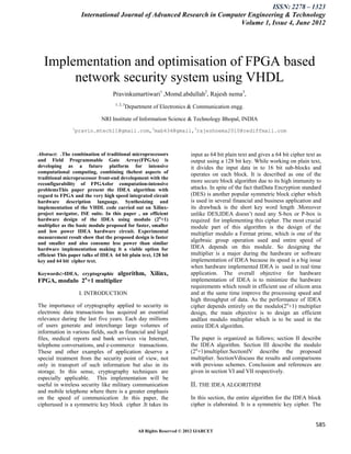
Figure1. Basic structure of IDEA Cipher and its becoming increasingly important. Cryptographic
data flow algorithms like International Data Encryption Algorithm
(IDEA) is frequently used for secured transmission of
data. Modulo 2naddition and modulo (2n+1)
The security of IDEA depends on these three operations. multiplication are the crucial operations in the IDEA
The basic structure of IDEA cipher is shown in Figure . algorithm and also modulo (2n+ 1) arithmetic operations
The IDEA cipher consists of 8 rounds which are are used inFerment number transform computation.
identical in nature and a last output transformation Now a day, modulo arithmetic is frequently used in fault
round which is similar to upper half of any round. tolerant design of ad-hoc networks, digital and linear
Before the starting of 1st round, the input 64 bit plain convolution architectures. Apart from these, residue
text is divided into four 16 bit sub-blocks, X1, X2, X3 arithmetic is extremely efficient for image processing,
and X4 respectively. At the end of encryption phase, speech processing and transforms all of which are
four 16 bit sub-blocks of cipher text is created. Each extremely important in today‟s high dense computing
round uses six 16 bit sub-key blocks Z1 (n), Z2 (n) ,… , world.
586
All Rights Reserved © 2012 IJARCET
3. ISSN: 2278 – 1323
International Journal of Advanced Research in Computer Engineering & Technology
Volume 1, Issue 4, June 2012
IV.Proposed multiplier Let we understand This proposed multiplier using an
example for n=4 bit .the result (worst case) of
There are several multipliers existing for idea. Here we multiplication of two 4 bit number is 11111111(255)10 if
are presenting a new kind of modulo multiplier which is we calculate the mod 2n+1 (n=4)of this number then we
highly optimized as compared to previous one. The get the result is 00000000 (0)10.
description for proposed multiplier is as follows. In
general if we multiply the two n bit number ,then we get
2n bit number. Store this 2n bit number(result) in to
temporary register ie.t1,then make the length of
modulo(2n+1) equal to the length of 2n bit number ie.t1,
by consented zeroes(„0‟s) after the LSB bit of the
modulo(2n+1) and store this value into t2. Here we
defining the subsequent steps by block/flow diagram,
which is easy to understand. Here we take n=16…
Figure 3. example of two 4 bit number
V. RESULT
The parameter used to evaluate the quality of the
modulo multiplier are slices, internal multiplier used
and throughput per slices(TPS). Xilinx synthesis tools
measure the amount of used resources in terms of
Configurable Logic Block ( CLB‟s) or slices, where one
CLB is ebullient to four slices. The principal difference
between the reportsfrom different manufacture is the
basic element definition and its interconnection with
others of the same kind. For this reason, theresults of the
synthesis are compared with other implementations that
have been targeted on chips from the same
manufacturer.
Figure 2.Block diagram/flow diagram of proposed multiplier
587
All Rights Reserved © 2012 IJARCET
4. ISSN: 2278 – 1323
International Journal of Advanced Research in Computer Engineering & Technology
Volume 1, Issue 4, June 2012
TABLE 1: Synthesis result . DeviceVirtex2P-XC2VP40-FG676-7
PARAMET
Used Available Utilization
ERS
Number of 4
input LUT‟s 376 93,184 1%
Number of
slices 192 46,592 1%
Number of
bonded IOB‟s 48 824 5%
Number of mul
18*18s 1 168 1%
Figure 5.RTLview of proposed multiplier.
The results of the implimantation in terms of area & SPEED
are summarized in table 1.table 2 represent the results
obtained with other hardware implimantation.
Table 2.Performance result for comparison
Preferred Multiplier Multiplier
Proposed Figure 6.Internal view (RTL) of multiplier.
FPGA
multiplier
device [1] [2]
Number of The overall effect of the proposed multiplier is
internal
Multiplier 4 3 1 enhancement of throughput( 61.89 Mbps) of the entire
used IDEA .i.e . international data encryption algoritham.
And the device utilisation is 36%.A simulation of our
Number of IDEA chip with the proposed new modulo multiplier
slices(LUT)u 264 - 192 designwas performed. The timing simulation reveals
sed
that the proposed structure has a time delay of 56.5ns.
Maximum
8.25
clock 10.9MHz 18.12MHz
frequency MHz
VI. CONCLUSION
Size of bits
processed 16 16 16
703.36Mb 1159.68 This paper presents a high speed, low area, cost
Throughput -
ps Mbps effective idea cipher for encryption using a basic 64-
bit iterative architecture, targeted towards the Spartan
family of FPGAs. This architecture is based on
previous work on the cipher design. In this work a
modulo(2n+1) multiplier is modified. The number of
clock cycle required to encrypt a single block has
been reduced and amount of hardware resources has
been optimized. The architecture needs fewer logic
cells than other cipher and uses as few memory blocks
as possible.
Figure 4. Simulation window of implementied multiplier
588
All Rights Reserved © 2012 IJARCET
5. ISSN: 2278 – 1323
International Journal of Advanced Research in Computer Engineering & Technology
Volume 1, Issue 4, June 2012
Figure 6. Internal view of IDEA ( 9 ROUND‟s)
REFERENCES Comparison analysis”,593-604,3rd
November,2004,Elsevier
[1] Sourav Mukherjee and BibhudattaSahoo, “A Hardware [11] Thaduri,M.,Yoo,S. and Gaede,R, “ An Efficient
implementation of IDEA cryptosystem using a recursive Implementation ofIDEA encryption algorithm using
multiplication approach.”, International Conference on VHDL”, ©2004 Elsevier.
Electronic Systems (ICES-2011), pp 383 - 389, 2011, [12] Allen Michalski1, Kris Gaj, Tarek El-Ghazawi, “An
[2] YI-JUNG CHEN1, DYI-RONG DUH2 AND Implementation Comparison of an IDEA Encryption
YUNGHSIANG SAM HAN, “Improved Modulo (2n + 1) Cryptosystemon Two General-Purpose Reconfigurable
Multiplier for IDEA”, journal of information science and Computers”
engineering 23, 907-919 (2007). [13] SarangDharmapurikar and John Lockwood, “Fast and
[3] R. Zimmermann, A. Curiger, H. Bonnenberg, H. Kaeslin, Scalable Pattern Matching for Network Intrusion
N. Felber, and W. Fichtner,“A 177mb/s VLSI Detection Systems”IEEE Journal on Selected Areas in
implementation of the international data encryption Communications: Oct. 2006, Volume: 24, pp. 1781- 1792
algorithm,”IEEE Journal of Solid-State Circuits, Vol. 29, .
1994, pp. 303-307. [14] Chiranth E, Chakravarthy H.V.A, Naga mohanareddy P,
[4] Modugu.R, Yong-Bin Kim, MinsuChoi,“Design and Umesh T.H, Chethan Kumar M., “Implementation of RSA
performance measurement of efficient IDEA crypto- Cryptosystem Using Verilog” International Journal of
hardware using novel modular arithmetic components”, Scientific & Engineering Research Volume 2, Issue 5,
Instrumentation and Measurement Technology Conference May-2011.
(I2MTC), 2010 IEEE, 3-6 May2010,pp1222-1227.
[5] Rahul Ranjan and I. Poonguzhali, “VLSI Implementation Authors :
of IDEA Encryption Algorithm”, Mobile and Pervasive
Computing (CoMPC–2008). 1. Prof. Rajesh Nema pursuing Ph.D., & currently working
[6] SomayehTimarchi, KeivanNavi, “Improved Modulo 2n+1 as Prof. in NIIST Bhopal. MP.(INDIA).
Adder Design”, International Journal of Computer and
Information Engineering 2:7 2008. 2. Momd. Abdullah BE ,M.Tech and currently working as
[7] X.Lai and J.L Massey “A Proposal for a New Block Prof. in NIIST Bhopal. MP.(INDIA
Encryption Standard,” in advances in Cryptology –
EUROCRYPT 90,Berlia,Germany: Springer Verlag pp. 3. Pravin Kumar Tiwari BE in Electronics & communication,
389-404, 1990. currently perusing M.Tech in Micro electronics & vlsi
[8] AnttiH¨am¨al¨ainen, MattiTommiska, and JormaSkytt¨, design. From NIIST Bhopal. MP.(INDIA)
“6.78 Gigabits per Second Implementation of the IDEA
Cryptographic Algorithm”,2002 Springer-Verlag, pages
760-769.
[9] M.P. Leong, O.Y.H. Cheung, K.H.Tsoi and P.H.W.Leong
“ABit Serial Implementation of the International Data
Encryption Algorithm IDEA” ©IEEE 2000.
[10] P. Kitsos, N. Sklavos, M.D. Galanis, O. Koufopavlou , “64
Bit Block ciphers: Hardware Implementations and
589
All Rights Reserved © 2012 IJARCET
![ISSN: 2278 – 1323
International Journal of Advanced Research in Computer Engineering & Technology
Volume 1, Issue 4, June 2012
block size of data on which IDEA operates, is of 64 bit Z6(n).which are made from the input 128 bit key. The
and the key size is of 128 bits. But all data operations in super-script n denotes the nth round. The output
IDEA cipher are in 16 bit unsigned integers. The length transformation phase, which is considered as 9th or the
of the incoming data should be either in normal in last round, uses 4 sub-keys, Z1 (9), Z1 (9), Z1 (9), Z1 (9).
integer multiple of 64 bits or if not, is made by using Every round except the 1st round uses the output sub-
padding bits. At the end of the algorithm, a 64 bit cipher blocks produced in the previous round. In between
text is created. every round, the 2nd and the 3rd sub-blocks are
IDEA is based on mixing operation of three different swapped. The entire algorithm uses only three different
algebraic groups which are algebraic group operations which are XOR, addition
modulo 2n and multiplication modulo (2n+1). The
o XOR (bitwise). encryption phase of IDEA thus uses [(8*6) + 4] i.e. 52
o Addition modulo 2n. sub-key blocks, which are made from the 128 bit input
o Multiplication modulo (2n + 1). key. As IDEA involves only algebraic operations, no
look-up tables or S-Boxes are used like DES or AES.
The decryption phase of IDEA is identical to that of
the encryption phase. It uses the same sequence of
operations as in the encryption phase. The only change
is that the sub-keys are reversed and are slightly
different. That means the sub-keys which are used in
round 1 during encryption phase are manipulated during
last round of decryption phase. The subkeys used in
decryption are either additive or multiplicative inverse
of the sub-keys used in the encryption phase.
III. Modulo 2n+1 multiplier
Modulo 2n+1 multiplier is one of the critical
components in applications in the area of digital signal
processing, data encryption and residue arithmetic that
demand high-speed and low-power operation. In this
paper, efficient hardware architecture of modulo (2n+ 1
)multiplier is proposed and validated to address the
demand. The proposed modulo (2n+1) multiplier has
three major functional modules including partial
products generation module, partial products reduction
module and final stage addition module. Modulo
arithmetic has been widely used in various applications
such as digital signal processing where the residue
arithmetic is used for digital filter design. Also, the
number of wireless and internet communication nodes
has grown rapidly. The confidentiality and the security
of the data transmitted over these channels has
Figure1. Basic structure of IDEA Cipher and its becoming increasingly important. Cryptographic
data flow algorithms like International Data Encryption Algorithm
(IDEA) is frequently used for secured transmission of
data. Modulo 2naddition and modulo (2n+1)
The security of IDEA depends on these three operations. multiplication are the crucial operations in the IDEA
The basic structure of IDEA cipher is shown in Figure . algorithm and also modulo (2n+ 1) arithmetic operations
The IDEA cipher consists of 8 rounds which are are used inFerment number transform computation.
identical in nature and a last output transformation Now a day, modulo arithmetic is frequently used in fault
round which is similar to upper half of any round. tolerant design of ad-hoc networks, digital and linear
Before the starting of 1st round, the input 64 bit plain convolution architectures. Apart from these, residue
text is divided into four 16 bit sub-blocks, X1, X2, X3 arithmetic is extremely efficient for image processing,
and X4 respectively. At the end of encryption phase, speech processing and transforms all of which are
four 16 bit sub-blocks of cipher text is created. Each extremely important in today‟s high dense computing
round uses six 16 bit sub-key blocks Z1 (n), Z2 (n) ,… , world.
586
All Rights Reserved © 2012 IJARCET](data:image/gif;base64,R0lGODlhAQABAIAAAAAAAP///yH5BAEAAAAALAAAAAABAAEAAAIBRAA7)