SlideShare uma empresa Scribd logo
1 de 29
°2/17/2020
Mahasiswa dapat menjelaskan cara
kerja komponen dasar rangkaian
Sequential, yaitu Latch dan Flip-flop.
°2/17/2020
Overview
°2/17/2020
 Circuits require memory to store intermediate
data
 Sequential circuits use a periodic signal to
determine when to store values.
◦ A clock signal can determine storage times
◦ Clock signals are periodic
 Single bit storage element is a flip flop
 A basic type of flip flop is a latch
 Latches are made from logic gates
◦ NAND, NOR, AND, OR, Inverter
°2/17/2020
 Hasil operasi Rangkaian Logika Kombinasional adalah
respon terhadap kombinasi input yang diberikan.
 Hanya bisa menjumlahkan dua bilangan.
 Untuk menjumlahkan bilangan ketiga, diperlukan
penyimpanan informasi hasil penjumlahan
sebelumnya.
▪ Contoh : 2+1 +5
▪ 2 + 1 = 3 maka 3 disimpan di dalam memory, kemudian :
▪ 3 + 5 = 8 (a sequential operation);
 To handle this, we need sequential logic capable of storing
intermediate (and final) results.
°2/17/2020
°2/17/2020
Combinational
circuit Flip
Flops
OutputsInputs
Next
state
Present
state
Timing signal
(clock)
Clock
Clock
a periodic external event (input)
synchronizes when current state changes happen
keeps system well-behaved
makes it easier to design and build large systems
°2/17/2020
1 1
1 0
0 1
0 0
S R Q Q’
0 1
1 0 Set
1 0 Stable
0 1 Reset
0 0 Undefined
R (reset)
Q
Q
S (set)
° S-R latch made from cross-coupled NORs
° If Q = 1, set state
° If Q = 0, reset state
° Usually S=0 and R=0
° S=1 and R=1 generates unpredictable results
°2/17/2020
S
R
Q
Q’
0 0
0 1
1 0
1 1
S R Q Q’
0 1
1 0 Set
1 0 Store
0 1 Reset
1 1 Disallowed
° Latch made from cross-coupled NANDs
° Sometimes called S’-R’ latch
° Usually S=1 and R=1
° S=0 and R=0 generates unpredictable results
°2/17/2020
° Occasionally, desirable to avoid latch changes
° C = 0 disables all latch state changes
° Control signal enables data change when C = 1
° Right side of circuit same as ordinary S-R latch.
Latch operation
enabled by
C
Input sampling
enabled by gates
°2/17/2020
R’
S’
Q’
Q
C’
Outputs change
when C is low:
RESET and SET
Otherwise: HOLD
Latch is level-sensitive, in regards to C
Only stores data if C’ = 0
°2/17/2020
Q
Q’
C
D S
R
X
Y
X Y C Q Q’
0 0 1 Q0 Q0’ Store
0 1 1 0 1 Reset
1 0 1 1 0 Set
1 1 1 1 1 Disallowed
X X 0 Q0 Q0’ Store
0 1 0 1
1 1 1 0
X 0 Q0 Q0’
D C Q Q’
° Q0 indicates the previous state (the previously stored value)
°2/17/2020
Q
Q’
C
D S
R
X
Y
0 1 0 1
1 1 1 0
X 0 Q0 Q0’
D C Q Q’
° Input value D is passed to output Q when C is high
° Input value D is ignored when C is low
°2/17/2020
E
x
Latches on following
edge of clock
E
D
Q
C
x
z
z
° Z only changes when E is high
° If E is high, Z will follow X
°2/17/2020
E
x
Latches on following
edge of clock
E
D
Q
C
x
z
z
° The D latch stores data indefinitely, regardless of
input D values, if C = 0
° Forms basic storage element in computers
°2/17/2020
° SR latch is based on NOR gates
° S’R’ latch based on NAND gates
° D latch can be based on either.
° D latch sometimes called transparent latch
 Latches are based on combinational gates (e.g.
NAND, NOR)
 Latches store data even after data input has
been removed
 S-R latches operate like cross-coupled inverters
with control inputs (S = set, R = reset)
 With additional gates, an S-R latch can be
converted to a D latch (D stands for data)
 D latch is simple to understand conceptually
◦ When C = 1, data input D stored in latch and output as Q
◦ When C = 0, data input D ignored and previous latch value output at Q
°2/17/2020
 Latches respond to trigger levels on control inputs
◦ Example: If G = 1, input reflected at output
 Difficult to precisely time when to store data with
latches
 Flip flops store data on a rising or falling trigger
edge.
◦ Example: control input transitions from 0 -> 1, data input appears at output
◦ Data remains stable in the flip flop until until next rising edge.
 Different types of flip flops serve different functions
 Flip flops can be defined with characteristic
functions.
°2/17/2020
°2/17/2020
Lo-Hi edgeHi-Lo edge
° What if the output only changed on a C transition?
C
D Q
Q’
0 0 1
1 1 0
X 0 Q0 Q0’
D C Q Q’
Positive edge triggered
°2/17/2020
° Consider two latches combined together
° Only one C value active at a time
° Output changes on falling edge of the clock
°2/17/2020
D gets latched to Q on the rising edge of the clock.
° Stores a value on the positive edge of C
° Input changes at other times have no effect on
output
C
D Q
Q’
0 0 1
1 1 0
X 0 Q0 Q0’
D C Q Q’
Positive edge triggered
°2/17/2020
° Stores a value on the positive edge of C
° Input changes at other times have no effect on
output
Positive Edge-Triggered J-K Flip-Flop
0 0 Q0 Q0’
0 1 0 1
1 0 1 0
1 1 TOGGLE
QJ Q’CLKK°Created from D flop
°J sets
°K resets
°J=K=1 -> invert output
°2/17/2020
°2/17/2020
° Two data inputs, J and K
° J -> set, K -> reset, if J=K=1 then toggle output
Characteristic Table
2. Positive Edge-Triggered T Flip-Flop
0 Q0 Q0’
1 TOGGLE
Q Q’CT
°Created from D flop
°T=0 -> keep current
°K resets
°T=1 -> invert current
°2/17/2020
°2/17/2020
• J, K are synchronous inputs
o Effects on the output are synchronized with the CLK input.
• Asynchronous inputs operate independently of the synchronous
inputs and clock
o Set the FF to 1/0 states at any time.
°2/17/2020
°2/17/2020
° Flip flops store outputs from combinational logic
° Multiple flops can store a collection of data
 Flip flops are powerful storage elements
◦ They can be constructed from gates and latches!
 D flip flop is simplest and most widely used
 Asynchronous inputs allow for clearing and
presetting the flip flop output
 Multiple flops allow for data storage
◦ The basis of computer memory!
 Combine storage and logic to make a
computation circuit
 Next time: Analyzing sequential circuits.
°2/17/2020
 Gunakan Multisim untuk merancang
rangkaian penyimpan 3 bit data secara
paralel.
 Kemudian data tersebut dihapus
 Diisi lagi dengan data baru
°2/17/2020

Mais conteúdo relacionado

Mais procurados

Latches and flip flop
Latches and flip flopLatches and flip flop
Latches and flip flopShuaib Hotak
 
2.3 sequantial logic circuit
2.3 sequantial logic circuit2.3 sequantial logic circuit
2.3 sequantial logic circuitWan Afirah
 
Rs flipflop or SR flipFlop
Rs flipflop or SR flipFlop Rs flipflop or SR flipFlop
Rs flipflop or SR flipFlop Easy n Inspire L
 
Lec3 Intro to Computer Engineering by Hsien-Hsin Sean Lee Georgia Tech -- CMO...
Lec3 Intro to Computer Engineering by Hsien-Hsin Sean Lee Georgia Tech -- CMO...Lec3 Intro to Computer Engineering by Hsien-Hsin Sean Lee Georgia Tech -- CMO...
Lec3 Intro to Computer Engineering by Hsien-Hsin Sean Lee Georgia Tech -- CMO...Hsien-Hsin Sean Lee, Ph.D.
 
Edge Trigged Flip Flops
Edge Trigged Flip FlopsEdge Trigged Flip Flops
Edge Trigged Flip FlopsFaizan Janjua
 
Flip-Flop (Clocked Bistable)
Flip-Flop (Clocked Bistable)Flip-Flop (Clocked Bistable)
Flip-Flop (Clocked Bistable)Aravir Rose
 
Logic Design - Chapter 6: Flip Flops
Logic Design - Chapter 6: Flip FlopsLogic Design - Chapter 6: Flip Flops
Logic Design - Chapter 6: Flip FlopsGouda Mando
 
Clocked Sequential circuit analysis and design
Clocked Sequential circuit analysis and designClocked Sequential circuit analysis and design
Clocked Sequential circuit analysis and designDr Naim R Kidwai
 
Sequential logic circuit
Sequential logic circuitSequential logic circuit
Sequential logic circuitAswiniT3
 
Understanding Flip Flops
Understanding Flip FlopsUnderstanding Flip Flops
Understanding Flip Flopsgavhays
 
Combinational circuits
Combinational circuitsCombinational circuits
Combinational circuitsAneeq Malik
 
Introduction state machine
Introduction state machineIntroduction state machine
Introduction state machineShreyans Pathak
 
Designing Clocked Synchronous State Machine
Designing Clocked Synchronous State MachineDesigning Clocked Synchronous State Machine
Designing Clocked Synchronous State MachineAbhilash Nair
 
Lec9 Intro to Computer Engineering by Hsien-Hsin Sean Lee Georgia Tech -- Com...
Lec9 Intro to Computer Engineering by Hsien-Hsin Sean Lee Georgia Tech -- Com...Lec9 Intro to Computer Engineering by Hsien-Hsin Sean Lee Georgia Tech -- Com...
Lec9 Intro to Computer Engineering by Hsien-Hsin Sean Lee Georgia Tech -- Com...Hsien-Hsin Sean Lee, Ph.D.
 
Logic Design - Chapter 7: Sequential Circuit Analysis and Design
Logic Design - Chapter 7: Sequential Circuit Analysis and DesignLogic Design - Chapter 7: Sequential Circuit Analysis and Design
Logic Design - Chapter 7: Sequential Circuit Analysis and DesignGouda Mando
 

Mais procurados (18)

Latches and flip flop
Latches and flip flopLatches and flip flop
Latches and flip flop
 
2.3 sequantial logic circuit
2.3 sequantial logic circuit2.3 sequantial logic circuit
2.3 sequantial logic circuit
 
Rs flipflop or SR flipFlop
Rs flipflop or SR flipFlop Rs flipflop or SR flipFlop
Rs flipflop or SR flipFlop
 
Lec3 Intro to Computer Engineering by Hsien-Hsin Sean Lee Georgia Tech -- CMO...
Lec3 Intro to Computer Engineering by Hsien-Hsin Sean Lee Georgia Tech -- CMO...Lec3 Intro to Computer Engineering by Hsien-Hsin Sean Lee Georgia Tech -- CMO...
Lec3 Intro to Computer Engineering by Hsien-Hsin Sean Lee Georgia Tech -- CMO...
 
Edge Trigged Flip Flops
Edge Trigged Flip FlopsEdge Trigged Flip Flops
Edge Trigged Flip Flops
 
Flip-Flop (Clocked Bistable)
Flip-Flop (Clocked Bistable)Flip-Flop (Clocked Bistable)
Flip-Flop (Clocked Bistable)
 
Lect19 Engin112
Lect19 Engin112Lect19 Engin112
Lect19 Engin112
 
Logic Design - Chapter 6: Flip Flops
Logic Design - Chapter 6: Flip FlopsLogic Design - Chapter 6: Flip Flops
Logic Design - Chapter 6: Flip Flops
 
Clocked Sequential circuit analysis and design
Clocked Sequential circuit analysis and designClocked Sequential circuit analysis and design
Clocked Sequential circuit analysis and design
 
Sequential logic circuit
Sequential logic circuitSequential logic circuit
Sequential logic circuit
 
Understanding Flip Flops
Understanding Flip FlopsUnderstanding Flip Flops
Understanding Flip Flops
 
Combinational circuits
Combinational circuitsCombinational circuits
Combinational circuits
 
Introduction state machine
Introduction state machineIntroduction state machine
Introduction state machine
 
Flip flops
Flip flopsFlip flops
Flip flops
 
Designing Clocked Synchronous State Machine
Designing Clocked Synchronous State MachineDesigning Clocked Synchronous State Machine
Designing Clocked Synchronous State Machine
 
Lec9
Lec9Lec9
Lec9
 
Lec9 Intro to Computer Engineering by Hsien-Hsin Sean Lee Georgia Tech -- Com...
Lec9 Intro to Computer Engineering by Hsien-Hsin Sean Lee Georgia Tech -- Com...Lec9 Intro to Computer Engineering by Hsien-Hsin Sean Lee Georgia Tech -- Com...
Lec9 Intro to Computer Engineering by Hsien-Hsin Sean Lee Georgia Tech -- Com...
 
Logic Design - Chapter 7: Sequential Circuit Analysis and Design
Logic Design - Chapter 7: Sequential Circuit Analysis and DesignLogic Design - Chapter 7: Sequential Circuit Analysis and Design
Logic Design - Chapter 7: Sequential Circuit Analysis and Design
 

Semelhante a Sequential circuits

Digital_Electronics_Module_4_Sequential_Circuits v0.6.pptx
Digital_Electronics_Module_4_Sequential_Circuits v0.6.pptxDigital_Electronics_Module_4_Sequential_Circuits v0.6.pptx
Digital_Electronics_Module_4_Sequential_Circuits v0.6.pptxUtsavDas21
 
5.8 Integrated circuits
5.8 Integrated circuits5.8 Integrated circuits
5.8 Integrated circuitslpapadop
 
Dee2034 chapter 4 flip flop for students part
Dee2034 chapter 4 flip flop  for students partDee2034 chapter 4 flip flop  for students part
Dee2034 chapter 4 flip flop for students partSITI SABARIAH SALIHIN
 
SEQUENTIAL CIRCUITS -Module 5 (1).pptx
SEQUENTIAL CIRCUITS -Module 5 (1).pptxSEQUENTIAL CIRCUITS -Module 5 (1).pptx
SEQUENTIAL CIRCUITS -Module 5 (1).pptxThanmayiKumar
 
Chapter 4 flip flop for students
Chapter 4 flip flop for studentsChapter 4 flip flop for students
Chapter 4 flip flop for studentsCT Sabariah Salihin
 
Digital design slides for engineering
Digital  design   slides for engineeringDigital  design   slides for engineering
Digital design slides for engineeringkasheen2803
 
Digital clock presentation
Digital clock presentationDigital clock presentation
Digital clock presentationAditya Jha ✅
 
Aeav 301 lec 19
Aeav 301 lec 19Aeav 301 lec 19
Aeav 301 lec 190mehdi
 
8.flip flops and registers
8.flip flops and registers8.flip flops and registers
8.flip flops and registersDeepak Sharma
 
15CS32 ADE Module 4
15CS32 ADE Module 415CS32 ADE Module 4
15CS32 ADE Module 4RLJIT
 
Lab 12 – Latches and Flip-Flops Mugisha OmaryLab 12 .docx
Lab 12 – Latches and Flip-Flops Mugisha OmaryLab 12 .docxLab 12 – Latches and Flip-Flops Mugisha OmaryLab 12 .docx
Lab 12 – Latches and Flip-Flops Mugisha OmaryLab 12 .docxDIPESH30
 

Semelhante a Sequential circuits (20)

Digital_Electronics_Module_4_Sequential_Circuits v0.6.pptx
Digital_Electronics_Module_4_Sequential_Circuits v0.6.pptxDigital_Electronics_Module_4_Sequential_Circuits v0.6.pptx
Digital_Electronics_Module_4_Sequential_Circuits v0.6.pptx
 
5.8 Integrated circuits
5.8 Integrated circuits5.8 Integrated circuits
5.8 Integrated circuits
 
Assignment#5
Assignment#5Assignment#5
Assignment#5
 
Dee2034 chapter 4 flip flop for students part
Dee2034 chapter 4 flip flop  for students partDee2034 chapter 4 flip flop  for students part
Dee2034 chapter 4 flip flop for students part
 
SEQUENTIAL CIRCUITS -Module 5 (1).pptx
SEQUENTIAL CIRCUITS -Module 5 (1).pptxSEQUENTIAL CIRCUITS -Module 5 (1).pptx
SEQUENTIAL CIRCUITS -Module 5 (1).pptx
 
Chapter 4 flip flop for students
Chapter 4 flip flop for studentsChapter 4 flip flop for students
Chapter 4 flip flop for students
 
Flip flops & registers
Flip flops & registersFlip flops & registers
Flip flops & registers
 
latchesandflipflops.ppt
latchesandflipflops.pptlatchesandflipflops.ppt
latchesandflipflops.ppt
 
Digital design slides for engineering
Digital  design   slides for engineeringDigital  design   slides for engineering
Digital design slides for engineering
 
Latches and flip flops
Latches and flip flopsLatches and flip flops
Latches and flip flops
 
Digital clock presentation
Digital clock presentationDigital clock presentation
Digital clock presentation
 
Aeav 301 lec 19
Aeav 301 lec 19Aeav 301 lec 19
Aeav 301 lec 19
 
8.flip flops and registers
8.flip flops and registers8.flip flops and registers
8.flip flops and registers
 
15CS32 ADE Module 4
15CS32 ADE Module 415CS32 ADE Module 4
15CS32 ADE Module 4
 
Chapter 6: Sequential Logic
Chapter 6: Sequential LogicChapter 6: Sequential Logic
Chapter 6: Sequential Logic
 
10529144.ppt
10529144.ppt10529144.ppt
10529144.ppt
 
JK flip flops
JK flip flopsJK flip flops
JK flip flops
 
Latches and flip flops
Latches and flip flopsLatches and flip flops
Latches and flip flops
 
Lab 12 – Latches and Flip-Flops Mugisha OmaryLab 12 .docx
Lab 12 – Latches and Flip-Flops Mugisha OmaryLab 12 .docxLab 12 – Latches and Flip-Flops Mugisha OmaryLab 12 .docx
Lab 12 – Latches and Flip-Flops Mugisha OmaryLab 12 .docx
 
lec7.ppt
lec7.pptlec7.ppt
lec7.ppt
 

Último

Employee leave management system project.
Employee leave management system project.Employee leave management system project.
Employee leave management system project.Kamal Acharya
 
Call Girls Wakad Call Me 7737669865 Budget Friendly No Advance Booking
Call Girls Wakad Call Me 7737669865 Budget Friendly No Advance BookingCall Girls Wakad Call Me 7737669865 Budget Friendly No Advance Booking
Call Girls Wakad Call Me 7737669865 Budget Friendly No Advance Bookingroncy bisnoi
 
Top Rated Call Girls In chittoor 📱 {7001035870} VIP Escorts chittoor
Top Rated Call Girls In chittoor 📱 {7001035870} VIP Escorts chittoorTop Rated Call Girls In chittoor 📱 {7001035870} VIP Escorts chittoor
Top Rated Call Girls In chittoor 📱 {7001035870} VIP Escorts chittoordharasingh5698
 
Thermal Engineering -unit - III & IV.ppt
Thermal Engineering -unit - III & IV.pptThermal Engineering -unit - III & IV.ppt
Thermal Engineering -unit - III & IV.pptDineshKumar4165
 
Thermal Engineering Unit - I & II . ppt
Thermal Engineering  Unit - I & II . pptThermal Engineering  Unit - I & II . ppt
Thermal Engineering Unit - I & II . pptDineshKumar4165
 
22-prompt engineering noted slide shown.pdf
22-prompt engineering noted slide shown.pdf22-prompt engineering noted slide shown.pdf
22-prompt engineering noted slide shown.pdf203318pmpc
 
Introduction to Serverless with AWS Lambda
Introduction to Serverless with AWS LambdaIntroduction to Serverless with AWS Lambda
Introduction to Serverless with AWS LambdaOmar Fathy
 
Thermal Engineering-R & A / C - unit - V
Thermal Engineering-R & A / C - unit - VThermal Engineering-R & A / C - unit - V
Thermal Engineering-R & A / C - unit - VDineshKumar4165
 
Unit 2- Effective stress & Permeability.pdf
Unit 2- Effective stress & Permeability.pdfUnit 2- Effective stress & Permeability.pdf
Unit 2- Effective stress & Permeability.pdfRagavanV2
 
XXXXXXXXXXXXXXXXXXXXXXXXXXXXXXXXXXXXXXXXXXXXXXXXXXXX
XXXXXXXXXXXXXXXXXXXXXXXXXXXXXXXXXXXXXXXXXXXXXXXXXXXXXXXXXXXXXXXXXXXXXXXXXXXXXXXXXXXXXXXXXXXXXXXXXXXXXXXX
XXXXXXXXXXXXXXXXXXXXXXXXXXXXXXXXXXXXXXXXXXXXXXXXXXXXssuser89054b
 
Unleashing the Power of the SORA AI lastest leap
Unleashing the Power of the SORA AI lastest leapUnleashing the Power of the SORA AI lastest leap
Unleashing the Power of the SORA AI lastest leapRishantSharmaFr
 
FULL ENJOY Call Girls In Mahipalpur Delhi Contact Us 8377877756
FULL ENJOY Call Girls In Mahipalpur Delhi Contact Us 8377877756FULL ENJOY Call Girls In Mahipalpur Delhi Contact Us 8377877756
FULL ENJOY Call Girls In Mahipalpur Delhi Contact Us 8377877756dollysharma2066
 
Call Girls In Bangalore ☎ 7737669865 🥵 Book Your One night Stand
Call Girls In Bangalore ☎ 7737669865 🥵 Book Your One night StandCall Girls In Bangalore ☎ 7737669865 🥵 Book Your One night Stand
Call Girls In Bangalore ☎ 7737669865 🥵 Book Your One night Standamitlee9823
 
Standard vs Custom Battery Packs - Decoding the Power Play
Standard vs Custom Battery Packs - Decoding the Power PlayStandard vs Custom Battery Packs - Decoding the Power Play
Standard vs Custom Battery Packs - Decoding the Power PlayEpec Engineered Technologies
 

Último (20)

Employee leave management system project.
Employee leave management system project.Employee leave management system project.
Employee leave management system project.
 
Call Girls Wakad Call Me 7737669865 Budget Friendly No Advance Booking
Call Girls Wakad Call Me 7737669865 Budget Friendly No Advance BookingCall Girls Wakad Call Me 7737669865 Budget Friendly No Advance Booking
Call Girls Wakad Call Me 7737669865 Budget Friendly No Advance Booking
 
Top Rated Call Girls In chittoor 📱 {7001035870} VIP Escorts chittoor
Top Rated Call Girls In chittoor 📱 {7001035870} VIP Escorts chittoorTop Rated Call Girls In chittoor 📱 {7001035870} VIP Escorts chittoor
Top Rated Call Girls In chittoor 📱 {7001035870} VIP Escorts chittoor
 
Thermal Engineering -unit - III & IV.ppt
Thermal Engineering -unit - III & IV.pptThermal Engineering -unit - III & IV.ppt
Thermal Engineering -unit - III & IV.ppt
 
Thermal Engineering Unit - I & II . ppt
Thermal Engineering  Unit - I & II . pptThermal Engineering  Unit - I & II . ppt
Thermal Engineering Unit - I & II . ppt
 
(INDIRA) Call Girl Meerut Call Now 8617697112 Meerut Escorts 24x7
(INDIRA) Call Girl Meerut Call Now 8617697112 Meerut Escorts 24x7(INDIRA) Call Girl Meerut Call Now 8617697112 Meerut Escorts 24x7
(INDIRA) Call Girl Meerut Call Now 8617697112 Meerut Escorts 24x7
 
22-prompt engineering noted slide shown.pdf
22-prompt engineering noted slide shown.pdf22-prompt engineering noted slide shown.pdf
22-prompt engineering noted slide shown.pdf
 
Introduction to Serverless with AWS Lambda
Introduction to Serverless with AWS LambdaIntroduction to Serverless with AWS Lambda
Introduction to Serverless with AWS Lambda
 
(INDIRA) Call Girl Aurangabad Call Now 8617697112 Aurangabad Escorts 24x7
(INDIRA) Call Girl Aurangabad Call Now 8617697112 Aurangabad Escorts 24x7(INDIRA) Call Girl Aurangabad Call Now 8617697112 Aurangabad Escorts 24x7
(INDIRA) Call Girl Aurangabad Call Now 8617697112 Aurangabad Escorts 24x7
 
(INDIRA) Call Girl Bhosari Call Now 8617697112 Bhosari Escorts 24x7
(INDIRA) Call Girl Bhosari Call Now 8617697112 Bhosari Escorts 24x7(INDIRA) Call Girl Bhosari Call Now 8617697112 Bhosari Escorts 24x7
(INDIRA) Call Girl Bhosari Call Now 8617697112 Bhosari Escorts 24x7
 
Thermal Engineering-R & A / C - unit - V
Thermal Engineering-R & A / C - unit - VThermal Engineering-R & A / C - unit - V
Thermal Engineering-R & A / C - unit - V
 
Unit 2- Effective stress & Permeability.pdf
Unit 2- Effective stress & Permeability.pdfUnit 2- Effective stress & Permeability.pdf
Unit 2- Effective stress & Permeability.pdf
 
XXXXXXXXXXXXXXXXXXXXXXXXXXXXXXXXXXXXXXXXXXXXXXXXXXXX
XXXXXXXXXXXXXXXXXXXXXXXXXXXXXXXXXXXXXXXXXXXXXXXXXXXXXXXXXXXXXXXXXXXXXXXXXXXXXXXXXXXXXXXXXXXXXXXXXXXXXXXX
XXXXXXXXXXXXXXXXXXXXXXXXXXXXXXXXXXXXXXXXXXXXXXXXXXXX
 
Call Girls in Ramesh Nagar Delhi 💯 Call Us 🔝9953056974 🔝 Escort Service
Call Girls in Ramesh Nagar Delhi 💯 Call Us 🔝9953056974 🔝 Escort ServiceCall Girls in Ramesh Nagar Delhi 💯 Call Us 🔝9953056974 🔝 Escort Service
Call Girls in Ramesh Nagar Delhi 💯 Call Us 🔝9953056974 🔝 Escort Service
 
Unleashing the Power of the SORA AI lastest leap
Unleashing the Power of the SORA AI lastest leapUnleashing the Power of the SORA AI lastest leap
Unleashing the Power of the SORA AI lastest leap
 
FULL ENJOY Call Girls In Mahipalpur Delhi Contact Us 8377877756
FULL ENJOY Call Girls In Mahipalpur Delhi Contact Us 8377877756FULL ENJOY Call Girls In Mahipalpur Delhi Contact Us 8377877756
FULL ENJOY Call Girls In Mahipalpur Delhi Contact Us 8377877756
 
Call Girls In Bangalore ☎ 7737669865 🥵 Book Your One night Stand
Call Girls In Bangalore ☎ 7737669865 🥵 Book Your One night StandCall Girls In Bangalore ☎ 7737669865 🥵 Book Your One night Stand
Call Girls In Bangalore ☎ 7737669865 🥵 Book Your One night Stand
 
Call Girls in Netaji Nagar, Delhi 💯 Call Us 🔝9953056974 🔝 Escort Service
Call Girls in Netaji Nagar, Delhi 💯 Call Us 🔝9953056974 🔝 Escort ServiceCall Girls in Netaji Nagar, Delhi 💯 Call Us 🔝9953056974 🔝 Escort Service
Call Girls in Netaji Nagar, Delhi 💯 Call Us 🔝9953056974 🔝 Escort Service
 
Call Now ≽ 9953056974 ≼🔝 Call Girls In New Ashok Nagar ≼🔝 Delhi door step de...
Call Now ≽ 9953056974 ≼🔝 Call Girls In New Ashok Nagar  ≼🔝 Delhi door step de...Call Now ≽ 9953056974 ≼🔝 Call Girls In New Ashok Nagar  ≼🔝 Delhi door step de...
Call Now ≽ 9953056974 ≼🔝 Call Girls In New Ashok Nagar ≼🔝 Delhi door step de...
 
Standard vs Custom Battery Packs - Decoding the Power Play
Standard vs Custom Battery Packs - Decoding the Power PlayStandard vs Custom Battery Packs - Decoding the Power Play
Standard vs Custom Battery Packs - Decoding the Power Play
 

Sequential circuits

  • 2. Mahasiswa dapat menjelaskan cara kerja komponen dasar rangkaian Sequential, yaitu Latch dan Flip-flop. °2/17/2020
  • 4.  Circuits require memory to store intermediate data  Sequential circuits use a periodic signal to determine when to store values. ◦ A clock signal can determine storage times ◦ Clock signals are periodic  Single bit storage element is a flip flop  A basic type of flip flop is a latch  Latches are made from logic gates ◦ NAND, NOR, AND, OR, Inverter °2/17/2020
  • 5.  Hasil operasi Rangkaian Logika Kombinasional adalah respon terhadap kombinasi input yang diberikan.  Hanya bisa menjumlahkan dua bilangan.  Untuk menjumlahkan bilangan ketiga, diperlukan penyimpanan informasi hasil penjumlahan sebelumnya. ▪ Contoh : 2+1 +5 ▪ 2 + 1 = 3 maka 3 disimpan di dalam memory, kemudian : ▪ 3 + 5 = 8 (a sequential operation);  To handle this, we need sequential logic capable of storing intermediate (and final) results. °2/17/2020
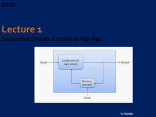
  • 6. °2/17/2020 Combinational circuit Flip Flops OutputsInputs Next state Present state Timing signal (clock) Clock Clock a periodic external event (input) synchronizes when current state changes happen keeps system well-behaved makes it easier to design and build large systems
  • 7. °2/17/2020 1 1 1 0 0 1 0 0 S R Q Q’ 0 1 1 0 Set 1 0 Stable 0 1 Reset 0 0 Undefined R (reset) Q Q S (set) ° S-R latch made from cross-coupled NORs ° If Q = 1, set state ° If Q = 0, reset state ° Usually S=0 and R=0 ° S=1 and R=1 generates unpredictable results
  • 8. °2/17/2020 S R Q Q’ 0 0 0 1 1 0 1 1 S R Q Q’ 0 1 1 0 Set 1 0 Store 0 1 Reset 1 1 Disallowed ° Latch made from cross-coupled NANDs ° Sometimes called S’-R’ latch ° Usually S=1 and R=1 ° S=0 and R=0 generates unpredictable results
  • 9. °2/17/2020 ° Occasionally, desirable to avoid latch changes ° C = 0 disables all latch state changes ° Control signal enables data change when C = 1 ° Right side of circuit same as ordinary S-R latch.
  • 10. Latch operation enabled by C Input sampling enabled by gates °2/17/2020 R’ S’ Q’ Q C’ Outputs change when C is low: RESET and SET Otherwise: HOLD Latch is level-sensitive, in regards to C Only stores data if C’ = 0
  • 11. °2/17/2020 Q Q’ C D S R X Y X Y C Q Q’ 0 0 1 Q0 Q0’ Store 0 1 1 0 1 Reset 1 0 1 1 0 Set 1 1 1 1 1 Disallowed X X 0 Q0 Q0’ Store 0 1 0 1 1 1 1 0 X 0 Q0 Q0’ D C Q Q’ ° Q0 indicates the previous state (the previously stored value)
  • 12. °2/17/2020 Q Q’ C D S R X Y 0 1 0 1 1 1 1 0 X 0 Q0 Q0’ D C Q Q’ ° Input value D is passed to output Q when C is high ° Input value D is ignored when C is low
  • 13. °2/17/2020 E x Latches on following edge of clock E D Q C x z z ° Z only changes when E is high ° If E is high, Z will follow X
  • 14. °2/17/2020 E x Latches on following edge of clock E D Q C x z z ° The D latch stores data indefinitely, regardless of input D values, if C = 0 ° Forms basic storage element in computers
  • 15. °2/17/2020 ° SR latch is based on NOR gates ° S’R’ latch based on NAND gates ° D latch can be based on either. ° D latch sometimes called transparent latch
  • 16.  Latches are based on combinational gates (e.g. NAND, NOR)  Latches store data even after data input has been removed  S-R latches operate like cross-coupled inverters with control inputs (S = set, R = reset)  With additional gates, an S-R latch can be converted to a D latch (D stands for data)  D latch is simple to understand conceptually ◦ When C = 1, data input D stored in latch and output as Q ◦ When C = 0, data input D ignored and previous latch value output at Q °2/17/2020
  • 17.  Latches respond to trigger levels on control inputs ◦ Example: If G = 1, input reflected at output  Difficult to precisely time when to store data with latches  Flip flops store data on a rising or falling trigger edge. ◦ Example: control input transitions from 0 -> 1, data input appears at output ◦ Data remains stable in the flip flop until until next rising edge.  Different types of flip flops serve different functions  Flip flops can be defined with characteristic functions. °2/17/2020
  • 18. °2/17/2020 Lo-Hi edgeHi-Lo edge ° What if the output only changed on a C transition? C D Q Q’ 0 0 1 1 1 0 X 0 Q0 Q0’ D C Q Q’ Positive edge triggered
  • 19. °2/17/2020 ° Consider two latches combined together ° Only one C value active at a time ° Output changes on falling edge of the clock
  • 20. °2/17/2020 D gets latched to Q on the rising edge of the clock. ° Stores a value on the positive edge of C ° Input changes at other times have no effect on output C D Q Q’ 0 0 1 1 1 0 X 0 Q0 Q0’ D C Q Q’ Positive edge triggered
  • 21. °2/17/2020 ° Stores a value on the positive edge of C ° Input changes at other times have no effect on output
  • 22. Positive Edge-Triggered J-K Flip-Flop 0 0 Q0 Q0’ 0 1 0 1 1 0 1 0 1 1 TOGGLE QJ Q’CLKK°Created from D flop °J sets °K resets °J=K=1 -> invert output °2/17/2020
  • 23. °2/17/2020 ° Two data inputs, J and K ° J -> set, K -> reset, if J=K=1 then toggle output Characteristic Table
  • 24. 2. Positive Edge-Triggered T Flip-Flop 0 Q0 Q0’ 1 TOGGLE Q Q’CT °Created from D flop °T=0 -> keep current °K resets °T=1 -> invert current °2/17/2020
  • 25. °2/17/2020 • J, K are synchronous inputs o Effects on the output are synchronized with the CLK input. • Asynchronous inputs operate independently of the synchronous inputs and clock o Set the FF to 1/0 states at any time.
  • 27. °2/17/2020 ° Flip flops store outputs from combinational logic ° Multiple flops can store a collection of data
  • 28.  Flip flops are powerful storage elements ◦ They can be constructed from gates and latches!  D flip flop is simplest and most widely used  Asynchronous inputs allow for clearing and presetting the flip flop output  Multiple flops allow for data storage ◦ The basis of computer memory!  Combine storage and logic to make a computation circuit  Next time: Analyzing sequential circuits. °2/17/2020
  • 29.  Gunakan Multisim untuk merancang rangkaian penyimpan 3 bit data secara paralel.  Kemudian data tersebut dihapus  Diisi lagi dengan data baru °2/17/2020