Graphene plasmonic couple to metallic antenna
•
0 gostou•630 visualizações

1. The document proposes a novel nanoantenna configuration using a metallic dipole antenna on top of an insulator layer, with a graphene sheet attached below the insulator. 2. By modifying the chemical potential of the graphene sheet using an applied gate voltage, the dispersion relation and optical conductivity of graphene can be tuned. 3. This allows the in-phase and out-of-phase coupling between the metallic plasmonics and graphene plasmonics to modify characteristics of the metal-graphene nanoantenna like its resonance frequency, near-field and far-field responses.
![12. A. N. Grigorenko, M. Polini, and K. S. Novoselov, “Graphene plasmonics,” Nat. Photonics 6, 749–758 (2012).
13. Y. Yao, M. A. Kats, P. Genevet, N. Yu, Y. Song, J. Kong, and F. Capasso, “Broad electrical tuning of graphene-
loaded plasmonic antennas,” Nano Lett. 13, 1257–1264 (2013).
14. F. Wang, Y. Zhang, C. Tian, C. Girit, A. Zettl, M. Crommie, and Y. R. Shen, “Gate-variable optical transitions in
graphene,” Science 320, 206–209 (2008).
15. M. Jablan, H. Buljan, and M. Soljaˇci´c, “Plasmonics in graphene at infrared frequencies,” Phys. Rev. B 80, 245435
(2009).
16. L. Novotny, “Effective wavelength scaling for optical antennas,” Phys. Rev. Lett. 98, 266802 (2007).
17. A. Al`u and N. Engheta, “Input impedance, nanocircuit loading, and radiation tuning of optical nanoantennas,”
Phys. Rev. Lett. 101, 043901 (2008).
18. P. B. Johnson and R. W. Christy, “Optical constants of the noble metals,” Phys. Rev. B 6, 4370–4379 (1972).
19. G. W. Hanson, “Dyadic green’s functions and guided surface waves for a surface conductivity model of
graphene,” J. Appl. Phys. 103, 064302 (2008).
20. A. Mock, “Pad´e approximant spectral fit for fdtd simulation of graphene in the near infrared,” Opt. Mater. Express
2, 771–781 (2012).
21. F. H. L. Koppens, D. E. Chang, and F. J. Garc´ıa de Abajo, “Graphene plasmonics: A platform for strong lightc-
matter interactions,” Nano Lett. 11, 3370–3377 (2011).
22. A.Taflove and S. Hagness, Computational Electrodynamics: The Finite-Difference Time-Domain Method (Artech
House, 2005).
23. X. Ren, Z. Huang, X. Wu, S. Lu, H. Wang, L. Wu, and S. Li, “High-order unified symplectic fdtd scheme for the
metamaterials,” Comput. Phys. Commun. 183, 1192–1200 (2012).
24. L. Tsang, J. A. Kong, and K. H. Ding, Scattering of Electromagnetic Waves: Theories and Applications (Wiley,
2000).
25. A. Yariv, “Coupled-mode theory for guided-wave optics,” IEEE J. Quantum Electron. 9, 919 – 933 (1973).
1. Introduction
Nanoantennas are, to some extent, analogue and evolving technology of the radiowave and
microwave antenna. But nanoantennas have lots of unique and novel characteristics mainly
owing to the existence of electron gas oscillations in metals. The behavior of strongly coupled
plasmas and the capability of manipulating light on the nanometer scale make nanoantennas
particularly useful in microscopy and spectroscopy [1], heat transfer [2] and photovoltaics [3,4],
etc. The above applications rely on the characteristics of nanoantennas involving the resonance
frequency, bandwidth, directivity, far-field radiation pattern, near-field distribution, and local
density of states. For instance, the existence of strong hot-spots in the feed gap would occur at
the resonant frequencies of dipole nanoantennas [5–7]. The characteristics of the nanoantenna
can be modified with geometrical size and shape as well as material composites. However, the
features cannot be dynamically tunable once the nanoantenna has been already fabricated.
Graphene is a monoatomic carbon with a honeycomb lattice which has attracted much re-
search interest in recent years [8–10]. Graphene has been used as a transparent electrode due
to the properties of high optical transmittance and conductivity [11]. Due to the forbidden in-
terband transitions by the Pauli blocking, the chemically or electrostatically doped graphene
supports strong plasmonic effects typically at the far-infrared or terahertz regime [12,13]. The
capability of dynamically modifying chemical potentials through tuning the gate voltage of the
graphene-metal nanoantenna as shown in the left side of Fig. 1 enables to fabricate controllable
devices by introducing the graphene sheet [14]. Applying this specific and unique property of
graphene to design nanoantennas could tune the characteristics and enhance the performances
of nanoantennas.
2. Structure and formulations
Here, we design a novel metal-graphene nanoantenna. One unit cell of the antenna is shown
in the right side of Fig. 1. The proposed architecture involves a conventional gold (Au) dipole
antenna comprising two Au arms separated by a feed gap, the graphene sheet, and aluminum
oxide (Al2O3) as an insulator inserted between the dipole antenna and graphene. The reso-
#198296 - $15.00 USD Received 25 Sep 2013; revised 3 Dec 2013; accepted 6 Dec 2013; published 16 Dec 2013
(C) 2013 OSA 30 December 2013 | Vol. 21, No. 26 | DOI:10.1364/OE.21.031824 | OPTICS EXPRESS 31825](data:image/gif;base64,R0lGODlhAQABAIAAAAAAAP///yH5BAEAAAAALAAAAAABAAEAAAIBRAA7)
Recomendados
Recomendados
Mais conteúdo relacionado
Mais procurados
Mais procurados (19)
Destaque
Destaque (12)
Semelhante a Graphene plasmonic couple to metallic antenna
Semelhante a Graphene plasmonic couple to metallic antenna (20)
Último
Último (20)
Graphene plasmonic couple to metallic antenna
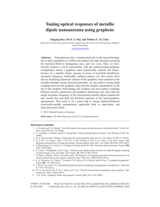
- 1. Tuning optical responses of metallic dipole nanoantenna using graphene Xingang Ren, Wei E. I. Sha, and Wallace C. H. Choy∗ Department of Electrical and Electronic Engineering, The University of Hong Kong, Pokfulam Road, Hong Kong ∗chchoy@eee.hku.hk Abstract: Nanoantennas play a fundamental role in the nanotechnology due to their capabilities to confine and enhance the light through converting the localized fields to propagating ones, and vice versa. Here, we theo- retically propose a novel nanoantenna with the metal-insulator-graphene configuration where a graphene sheet dynamically controls the charac- teristics of a metallic dipole antenna in terms of near-field distribution, resonance frequency, bandwidth, radiation pattern, etc. Our results show that by modifying dispersion relation of the graphene sheet attached to the insulator through tuning chemical potentials, we can achieve strong mode couplings between the graphene sheet and the metallic nanoantenna on the top of the insulator. Interestingly, the in-phase and out-of-phase couplings between metallic plasmonics and graphene plasmonics not only split the single resonance frequency of the conventional metallic dipole antenna but also modify the near-field and far-field responses of the metal-graphene nanoantenna. This work is of a great help to design high-performance electrically-tunable nanoantennas applicable both in nano-optics and nano-electronics fields. © 2013 Optical Society of America OCIS codes: (250.5403) Plasmonics;(230.4555) Coupled resonators. References and links 1. L. Novotny and S. J. Stranick, “Near-field optical microscopy and spectroscopy with pointed probes,” Annu. Rev. Phys. Chem. 57, 303–331 (2006). 2. J. A. Schuller, T. Taubner, and M. L. Brongersma, “Optical antenna thermal emitters,” Nat. Photonics 3, 658–661 (2009). 3. H. A. Atwater and A. Polman, “Plasmonics for improved photovoltaic devices,” Nat. Mater. 9, 205–213 (2010). 4. X. Li, W. C. H. Choy, L. Huo, F. Xie, W. E. I. Sha, B. Ding, X. Guo, Y. Li, J. Hou, J. You, and Y. Yang, “Dual plasmonic nanostructures for high performance inverted organic solar cells,” Adv. Mater. 24, 3046–3052 (2012). 5. P. Mhlschlegel, H.-J. Eisler, O. J. F. Martin, B. Hecht, and D. W. Pohl, “Resonant optical antennas,” Science 308, 1607–1609 (2005). 6. X. Chen, V. Sandoghdar, and M. Agio, “Nanofocusing radially-polarized beams for high-throughput funneling of optical energy to the near field,” Opt. Express 18, 10878–10887 (2010). 7. R. Zhao, L. Zhang, J. Zhou, T. Koschny, and C. M. Soukoulis, “Conjugated gammadion chiral metamaterial with uniaxial optical activity and negative refractive index,” Phys. Rev. B 83, 035105 (2011). 8. K. S. Novoselov, V. I. Falko, L. Colombo, P. R. Gellert, M. G. Schwab, and K. Kim, “A roadmap for graphene,” Nature 490, 192–200 (2012). 9. J. Zhu, Q. Liu, and T. Lin, “Manipulating light absorption of graphene using plasmonic nanoparticles,” Nanoscale 5, 7785–7789 (2013). 10. W. Lu, W. Zhu, H. Xu, Z. Ni, Z. Dong, and T. Cui, “Flexible transformation plasmonics using graphene,” Opt. Express 21, 10475–10482 (2013). 11. A. K. Geim, “Graphene: Status and prospects,” Science 324, 1530–1534 (2009). #198296 - $15.00 USD Received 25 Sep 2013; revised 3 Dec 2013; accepted 6 Dec 2013; published 16 Dec 2013 (C) 2013 OSA 30 December 2013 | Vol. 21, No. 26 | DOI:10.1364/OE.21.031824 | OPTICS EXPRESS 31824
- 2. 12. A. N. Grigorenko, M. Polini, and K. S. Novoselov, “Graphene plasmonics,” Nat. Photonics 6, 749–758 (2012). 13. Y. Yao, M. A. Kats, P. Genevet, N. Yu, Y. Song, J. Kong, and F. Capasso, “Broad electrical tuning of graphene- loaded plasmonic antennas,” Nano Lett. 13, 1257–1264 (2013). 14. F. Wang, Y. Zhang, C. Tian, C. Girit, A. Zettl, M. Crommie, and Y. R. Shen, “Gate-variable optical transitions in graphene,” Science 320, 206–209 (2008). 15. M. Jablan, H. Buljan, and M. Soljaˇci´c, “Plasmonics in graphene at infrared frequencies,” Phys. Rev. B 80, 245435 (2009). 16. L. Novotny, “Effective wavelength scaling for optical antennas,” Phys. Rev. Lett. 98, 266802 (2007). 17. A. Al`u and N. Engheta, “Input impedance, nanocircuit loading, and radiation tuning of optical nanoantennas,” Phys. Rev. Lett. 101, 043901 (2008). 18. P. B. Johnson and R. W. Christy, “Optical constants of the noble metals,” Phys. Rev. B 6, 4370–4379 (1972). 19. G. W. Hanson, “Dyadic green’s functions and guided surface waves for a surface conductivity model of graphene,” J. Appl. Phys. 103, 064302 (2008). 20. A. Mock, “Pad´e approximant spectral fit for fdtd simulation of graphene in the near infrared,” Opt. Mater. Express 2, 771–781 (2012). 21. F. H. L. Koppens, D. E. Chang, and F. J. Garc´ıa de Abajo, “Graphene plasmonics: A platform for strong lightc- matter interactions,” Nano Lett. 11, 3370–3377 (2011). 22. A.Taflove and S. Hagness, Computational Electrodynamics: The Finite-Difference Time-Domain Method (Artech House, 2005). 23. X. Ren, Z. Huang, X. Wu, S. Lu, H. Wang, L. Wu, and S. Li, “High-order unified symplectic fdtd scheme for the metamaterials,” Comput. Phys. Commun. 183, 1192–1200 (2012). 24. L. Tsang, J. A. Kong, and K. H. Ding, Scattering of Electromagnetic Waves: Theories and Applications (Wiley, 2000). 25. A. Yariv, “Coupled-mode theory for guided-wave optics,” IEEE J. Quantum Electron. 9, 919 – 933 (1973). 1. Introduction Nanoantennas are, to some extent, analogue and evolving technology of the radiowave and microwave antenna. But nanoantennas have lots of unique and novel characteristics mainly owing to the existence of electron gas oscillations in metals. The behavior of strongly coupled plasmas and the capability of manipulating light on the nanometer scale make nanoantennas particularly useful in microscopy and spectroscopy [1], heat transfer [2] and photovoltaics [3,4], etc. The above applications rely on the characteristics of nanoantennas involving the resonance frequency, bandwidth, directivity, far-field radiation pattern, near-field distribution, and local density of states. For instance, the existence of strong hot-spots in the feed gap would occur at the resonant frequencies of dipole nanoantennas [5–7]. The characteristics of the nanoantenna can be modified with geometrical size and shape as well as material composites. However, the features cannot be dynamically tunable once the nanoantenna has been already fabricated. Graphene is a monoatomic carbon with a honeycomb lattice which has attracted much re- search interest in recent years [8–10]. Graphene has been used as a transparent electrode due to the properties of high optical transmittance and conductivity [11]. Due to the forbidden in- terband transitions by the Pauli blocking, the chemically or electrostatically doped graphene supports strong plasmonic effects typically at the far-infrared or terahertz regime [12,13]. The capability of dynamically modifying chemical potentials through tuning the gate voltage of the graphene-metal nanoantenna as shown in the left side of Fig. 1 enables to fabricate controllable devices by introducing the graphene sheet [14]. Applying this specific and unique property of graphene to design nanoantennas could tune the characteristics and enhance the performances of nanoantennas. 2. Structure and formulations Here, we design a novel metal-graphene nanoantenna. One unit cell of the antenna is shown in the right side of Fig. 1. The proposed architecture involves a conventional gold (Au) dipole antenna comprising two Au arms separated by a feed gap, the graphene sheet, and aluminum oxide (Al2O3) as an insulator inserted between the dipole antenna and graphene. The reso- #198296 - $15.00 USD Received 25 Sep 2013; revised 3 Dec 2013; accepted 6 Dec 2013; published 16 Dec 2013 (C) 2013 OSA 30 December 2013 | Vol. 21, No. 26 | DOI:10.1364/OE.21.031824 | OPTICS EXPRESS 31825
- 3. light Au h Gap l w Graphene Au Al2O3 Fig. 1. A schematic pattern of metal-graphene nanoantennas. The chemical potential of graphene can be electrostatically tunable by changing the back gate voltage. The right figure shows a unit cell of the metal-graphene nanoantenna. The graphene sheet is deposited at the bottom of Al2O3. The geometric parameters are as l = 720 nm, w = 40 nm, h = 40 nm, and Gap = 20 nm. nant dipole antenna induces a strong confined field in the narrow feed gap, which is caused by the couplings between two metal arms [5, 15]. The arm lengths of the metallic dipole antenna should be carefully engineered so that the strong interaction between metallic plasmonics and graphene plasmonics occurs at the infrared regime. The geometric parameters of the Au dipole antenna are given in the caption of Fig. 1 for guaranteeing the resonant wavelength (3200 nm) to be in the infrared regime [16, 17]. The effective thickness of graphene in our numerical model, for simplicity and manipulation, is taken as d0 = 0.5 nm, which is sufficiently guaran- teed the convergence of our calculation. The electrical permittivities of the insulator and Au are ε = 3.065 and given by Johnson and Chrity [18], respectively. In addition, the insulator (with thickness of 4 nm) is inserted to reduce the electrical (quantum) tunneling effect from the graphene to metal. Consequently, the responses of the metal-graphene nanoantenna only depend on its optical effects governed by Maxwell’s equations. The surface conductivity of infinitesimally thin graphene is calculated by the Kubo formula as a function of the frequency (ω), chemical potential (μc), carrier scattering rate Gamma (Γ) and temperature (T) [19,20]: σ(ω,μc,Γ,T) = je2(ω − j2Γ) π¯h2 1 (ω − j2Γ)2 × ∞ 0 ε ∂ fd(ε) ∂ε − ∂ fd(−ε) ∂ε dε − ∞ 0 fd(−ε)− fd(ε) (ω − j2Γ)2 −4(ε/¯h)2 dε (1) where fd(ε) = {exp[(ε − μc)/kBT] + 1}−1 is the Fermi-Dirac distribution function and kB is the Boltzmann constant. The carrier scattering rate Gamma is set as Γ = 11 meV/¯h [20, 21]. It should be noted that: (i) The conductivity used in our simulation should be converted to the volume conductivity σ = σ/d0 where σ, σ are the surface and volume conductivities, respec- tively; and d0 is the effective thickness of the graphene sheet. (ii) This volume conductivity is contributed to the in-plane permittivity (ε ), while the out-of-plane permittivity is chosen to be the dielectric permittivity (ε⊥=2.5) [13]. (iii) The 1st and 2nd terms in the right side of Eq. (1) relate to the electron intraband relaxation and interband transition, respectively. As seen in Figs. 2(a) and 2(b), the real and imaginary part of the normalized surface conductivity of the graphene sheet are highly tunable with different chemical potential (by changing the gate volt- age). The imaginary part of the conductivity of graphene, corresponding to the real part of the in-plane permittivity (ε = εr − jσ/ωε0), becomes negative value near the visible regime with an appropriately adjusted chemical potential. In detailed, the imaginary part starts to be negative at the wavelengths of λ =820, 740, 680 nm corresponding to the chemical potentials μc =0.9, 1.0, 1.1 eV, respectively. Noted that the chemical potential (from 0.9 eV to 1.1 eV) used here #198296 - $15.00 USD Received 25 Sep 2013; revised 3 Dec 2013; accepted 6 Dec 2013; published 16 Dec 2013 (C) 2013 OSA 30 December 2013 | Vol. 21, No. 26 | DOI:10.1364/OE.21.031824 | OPTICS EXPRESS 31826
- 4. can be achieved by a high doping which could be promisingly obtained in near future experi- ments. Resembling noble metals, the highly doped graphene sheet with a negative permittivity will start to support transverse magnetic (TM) surface plasmon polariton (SPP), which opens a door for a strong light-matter interaction between the graphene and metallic nanostructures. 0 10 20 30 40 0.5 1 1.5 2 2.5 3 Propagation constant (109 m-1 ) Frequency(1015 rad/sec) 0.9 eV 1.0 eV 1.1 eV (a) (b) (c) (d) 100 200 300 400 500 -1 -0.5 0 0.5 Frequency (THz) Imaginarypart 0.9 eV 1.0 eV 1.1 eV 100 200 300 400 500 600 0 0.1 0.2 0.3 Frequency (THz) Realpart 0.9 eV 1.0 eV 1.1 eV x (nm) z(nm) 0 50 100 0 20 40 60 -1 -0.5 0 0.5 1 Dipole source Al2O3 Graphene SiO2 Fig. 2. The optical properties of graphene at different chemical potentials (μc = 0.9, 1.0, 1.1 eV). Other physical quantities are set as T = 300 K and Γ = 11 meV/¯h [20]. (a) The real part, (b) The imaginary parts of the normalized surface conductivity (defined as σ/σ0 and σ0 = e2/¯h) of the graphene sheet. (c) The analytical dispersion relation of the graphene sheet sandwiched by the semi-infinite insulator Al2O3 and SiO2. (d) The near field distribu- tions of the doped graphene sheet (μc =1.1 eV) inserted by 4 nm Al2O3 and 100 nm SiO2 (as shown in the inset) at the wavelength of 3000 nm. . The dispersion relation of the infinitely thin graphene sheet inserted between two dielectric media has been theoretically determined in the literature [15]. In our case, the graphene is sandwiched between Al2O3 and silicon oxide (SiO2). The dispersion relation of the sandwich configuration for the TM mode is given by β(ω) ≈ ε0 εr1 +εr2 2 2jω σ(ω) (2) where β(ω) is the propagation constant, ε0 is the permittivity of air, and εr1 and εr2 are the elec- trical permittivities of the two dielectric media and εr1 = 3.065 and εr2 = 2.25 for Al2O3 and SiO2, respectively. Moreover, ω is the angular frequency and σ(ω) is the surface conductivity of the graphene sheet. Figure 2(c) shows the dispersion relation of the Al2O3-graphene-SiO2 configuration for the TM SPP mode. It can be easily found that the plasmonic resonance is blue-shifted when the chemical potential increases from 0.9 eV to 1.1 eV. In addition, the near field is shown in Fig. 2 (d) for the thin graphene layer inserted by 4 nm Al2O3 and 100 nm SiO2 (the configuration is shown in the inset) which is much more close to our proposed configura- tion. The bounded plasmonic wave was found around the doped graphene sheet (μc =1.1 eV) at the wavelength of 3000 nm that is near the resonant wavelength of the Au dipole antenna. This will enable the mode couplings or hybridizations between the highly doped graphene sheet and the dipole nanoantenna. 3. Results and discussions The proposed metal-graphene nanoantenna is theoretically studied through rigorously solving Maxwell’s equations by finite-difference time-domain (FDTD) method [22, 23]. Within the #198296 - $15.00 USD Received 25 Sep 2013; revised 3 Dec 2013; accepted 6 Dec 2013; published 16 Dec 2013 (C) 2013 OSA 30 December 2013 | Vol. 21, No. 26 | DOI:10.1364/OE.21.031824 | OPTICS EXPRESS 31827
- 5. wavelength range of interest, the normalized extinction cross section (ECS) [24] is calculated and illustrated in Fig. 3(a). The single resonant peak due to the fundamental dipole mode of the dipole antenna without the graphene sheet is located at the wavelength of 3200 nm. After introducing the graphene layer, this resonant peak is blue-shifted [13], more importantly, the single resonant peak splits into two individual resonant peaks at the wavelengths of 2900 nm and 3050 nm for the metal-graphene hybrid antenna. According to the coupled mode theory [24, 25], the low resonant peak at the short wavelength of 2900 nm is attributed to the out- of-phase coupling between the surface wave of graphene and dipolar mode of nanoantennas, while in-phase coupling is contributed to the high resonant peak at the longer wavelength of 3050 nm. Besides, Fig. 4 shows the near-field E-field distribution of the hybrid nanoantenna with respect to the four wavelengths denoted by the arrows of Fig. 3(a). As indicated in Fig. 4, a very strong E-field is expected in the feed gap and the edges of the two Au arms when the incoming plane wave is polarized along the metal arms. The constructive interferences between two SPPs of the metallic arms not only produce a strong field enhancement at the gap but also introduce evanescent waves going down to the graphene sheet. The evanescent waves also offer additional momentums to excite the graphene plasmonics. Furthermore, compared to those in the insulator and metal, the near-field distributions corresponding to the dip between the two resonant peaks (denoted by the arrow 3 in Fig. 3(a)) is concentrated around the graphene sheet where light drives the coherent electron oscillations in the ultra-thin graphene sheet with a high mobility. This oscillation also plays an important role in forming the strong field confinement in the graphene sheet. 20 40 60 30 210 60 240 90 270 120 300 150 330 180 0 Normalized RCS w/o G w G 3000 3500 4000 0 50 100 150 200 250 Wavelength (nm) NormalizedECS 0 eV 0.9 eV 1.0 eV 2000 2500 3000 3500 4000 0 50 100 150 200 250 Wavelength (nm) NormalizedECS Gamma/2 Gamma 2Gamma (c) (b) (d) 2000 2500 3000 3500 4000 0 50 100 150 200 250 Wavelength (nm) NormalizedECS w/o G w G (a) 2 1 3 4 Fig. 3. The characteristics of the metallic dipole nanoantenna with and without the graphene sheet. Both the extinction cross section and radar cross section are normalized with the geo- metrical cross section area of the metallic dipole antenna (2w×l). (a) Extinction cross sec- tion. (b) The polar plot of the far-field radiation pattern. (c) Extinction Cross Section at dif- ferent chemical potentials.(d) Extinction Cross Section at different scattering rate Gamma (with μc =1.0 eV). With the graphene, the full width at half maximum (FWHM) of the extinction cross section (normalized to unity) is decreased by 18% for the hybrid nanoantenna. Another characteristic of the nanoantenna called normalized radar cross section (RCS) [24] or far-field radiation pattern from the reciprocal theorem, is also calculated and drawn in Fig. 3(b). The far-field radiation intensity has been drastically reduced by 70% due to the optical absorption induced by the graphene plasmonics. The most important property of the metal-graphene hybrid nanoantenna lies at its tunable or switch on/off feature which is also shown in Fig. 3(c). It is apparently seen that the high resonant peak at the longer wavelength is dynamically tunable through increas- #198296 - $15.00 USD Received 25 Sep 2013; revised 3 Dec 2013; accepted 6 Dec 2013; published 16 Dec 2013 (C) 2013 OSA 30 December 2013 | Vol. 21, No. 26 | DOI:10.1364/OE.21.031824 | OPTICS EXPRESS 31828
- 6. x (nm) z(nm) 0 500 1000 1500 0 20 40 60 80 x (nm) z(nm) 0 500 1000 1500 0 20 40 60 80 x (nm) z(nm) 0 500 1000 1500 0 20 40 60 80 x (nm) z(nm0 0 500 1000 1500 0 20 40 60 80 (a) (b) (c) (d) Fig. 4. The near-field distributions (in log scale) of the metal-graphene nanoantenna corre- sponding to the four wavelengths denoted by the arrows of Fig. 3(a). (a) 2500 nm; (b) 2900 nm; (c) 3000 nm; (d) 3050 nm. ing the chemical potential from 0.9 eV to 1.0 eV by increasing the gate voltage. Especially, the hybrid nanoantenna can be restored to the conventional metallic dipole antenna by simply employing an intrinsic graphene (μc=0 eV) or electrostatically tuning the chemical potential of graphene less than 0.6 eV. This provides a new opportunity to control the optical nanoan- tenna through nanoelectronics devices. In addition, we also investigate the carrier scattering rate Gamma (Γ) that could influence mode coupling of the proposed nanoantenna in terms of the normalized ECS. As shown in Fig. 3(d), the coherent mode coupling between the ultra-thin graphene and Au dipole antenna can be supported either by adopting a smaller carrier scattering rate Γ/2 or a larger carrier scattering rate 2Γ. A smaller carrier scattering induces significant resonance splitting. Contrarily, an increasing carrier scattering rate or Ohmic loss of graphene reduces the difference between the peak and valley of the normalized ECS and further slightly increases the bandwidth of the antenna. 4. Conclusion In summary, we have analyzed and designed a tunable metal-graphene hybrid nanoantenna. By dynamically tuning the chemical potential of graphene, the mode couplings between the doped graphene sheet and metallic nanoatenna can be obtained. The splitting resonance peaks of the hybrid nanoantenna confirm the strong interaction between the graphene plasmonics and metal plasmonics. The simulation results also reveal a strong field enhancement and confinement in the graphene sheet. Particularly, the near-field distribution, resonance frequency, bandwidth, and radiation pattern of the convectional metallic dipole antenna are strongly modified and highly tunable after the introduction of graphene. This work is helpful to design new electrically-tunable optical nanoantennas. Acknowledgments This work is supported by University Grant Council of the University of Hong Kong (Nos. 10401466, 201111159062), and the General Research Fund (HKU712010E and HKU711612E), the RGC-NSFC grant (N HKU709/12) from the Research Grants Council of Hong Kong Special Administrative Region, China. This work is also supported by the seed project funding of HKU (No. 201211159147). We also acknowledge Luzhou Chen and Lu Zhu for their fruitful discussions and valuable input. #198296 - $15.00 USD Received 25 Sep 2013; revised 3 Dec 2013; accepted 6 Dec 2013; published 16 Dec 2013 (C) 2013 OSA 30 December 2013 | Vol. 21, No. 26 | DOI:10.1364/OE.21.031824 | OPTICS EXPRESS 31829