
Recomendados
Mais conteúdo relacionado
Mais procurados
Mais procurados (20)
Destaque
Destaque (20)
Semelhante a Understanding semiconductor diodes
Semelhante a Understanding semiconductor diodes (20)
Mais de wengsung60
Último
Último (20)
Understanding semiconductor diodes
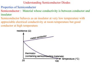
- 1. Understanding Semiconductor Diodes Properties of Semiconductor Semiconductor : Material whose conductivity is between conductor and insulator Semiconductor behaves as an insulator at very low temperature with appreciable electrical conductivity at room temperature but good conductor at high temperature
- 2. Pure Element Semiconductors: Silicon, germanium, boron, tellurium and selenium Compound Semiconductors: Lead sulphide, gallium arsenide, cadmium selenide and indium arsenide A silicon atom
- 3. Typical semiconductor materials are silicon and germanium. Each has 4 electrons in its outer orbital (outermost shell) Each electron in the outer orbital can form a covalent bond with one electron from outer orbital of another atom (Form four covalent bonds with four neighbouring atoms) When at high temperature, the thermal energy of the vibrating atoms causes some electrons to break free
- 4. For every electron that is broken free, there is a hole in the bonding structure. The atom is neutral, it has a complete set of protons and electrons, the hole behaves as if it has a positive charge.
- 5. Two types of charge carriers in a semiconductor: the electron and hole When electron is removed from a covalent bond, it leaves a vacancy (hole). An electron from a neighbouring atom can fill this vacancy, leaving neighbouring atom now with a vacancy. Therefore the vacancy (hole) can travel through the lattice and act as a charge carrier.
- 6. Doping of Semiconductor Doping: Process of adding a certain amount of specific impurities (dopants) to a crystalline lattice of semiconductor, to increase the conductivity. Type of semiconductors produced by doping: p-type semiconductor and n-type semiconductor p-type semiconductor
- 7. p-type doping (Create an abundance of holes in the material) By doping trivalent atoms such as boron, gallium or aluminium to replace some of the silicon atoms. One electron is missing from one of the four covalent bond The trivalent atoms are called acceptor atoms, because they accept any free electrons to fill the holes. When accepting an electron from its neighbouring atom, a hole is created due to deficiency of electron. If more trivalent atoms are added, there will be more holes than free electrons, hence holes are now majority carriers and free electrons are the minority carriers
- 8. n-type semiconductor (Produce abundance of electrons) By doping pentavalent atoms such as phosphorus, arsenic or antimony to replace some of the silicon atoms. Each of the pentavalent atoms will have four covalent bonds and one extra electron. A free electron is available as a charge carrier The pentavalent atom donates an extra electron it is therefore called the donor atom. The free electrons are the majority charge carriers and the holes are the minority charge carriers. n-type semiconductor
- 9. Semiconductor Diodes Semiconductor diode is an electronic device made from a p-n junction The region of p-type and n-type materials are called anode and cathode respectively A diode is a device that allows current to flow in one direction only
- 10. The depletion layer is formed when there is a decrease in the free electrons and holes in the region around the p-n junction. The electrons from the n-type material drift across the junction to fill in the holes in the p-type material. The holes from the p-type material drift in the opposite direction depletion layer
- 11. As a result the p-type region becomes more negative and the n-type becomes more positive. This result in a potential difference acting from the n-type to the p- type region across the junction The potential difference is called the junction voltage (it prevents the charge carriers from drifting across the junction)
- 12. In order for electric current to flow through the diode, the voltage applied across the diode must exceed the junction voltage The junction voltage for germanium and silicon are approximately 0.1V and 0.6 V respectively
- 13. Ways of connection of diodes Forward bias connection The p-type (anode) is connected to the positive terminal and the n- type (cathode) is connected to the negative terminal
- 14. When the potential difference supplied by the cell exceeds the junctions power, the holes from p-type material and the electrons from n-type material drift across the p-n junction The depletion layer becomes narrow and the resistance of the diode decreases, the bulbs lights up.
- 15. Reverse bias The n-type is connected to the positive terminal and the p-type is connected to the negative terminal
- 16. The reversed polarity causes a very small current to flow as both electrons and holes are pulled away from the junction The depletion layer becomes wider. The resistance of the diode becomes higher When the potential difference due to the widen depletion region equals the voltage of the battery, the current cease flowing completely, therefore the bulb does not light up
- 17. Diode as a rectifier A diode in forward bias only allows current to flow in one direction (from anode to cathode-act as a valve) A rectifier is an electrical device that converts alternating current to direct current A complete cycle of an a.c. consists of two half cycle: a positive half cycle and a negative half cycle
- 19. Two type of rectification: a) Half-wave rectification b) Full-wave rectification Half-wave rectification The current will only flow in the first half-cycle when the diode is forward bias and is blocked in the second half, when the diode is in reverse bias. Current flowing is half-wave rectified
- 20. Full-wave rectification When 4 diodes in the form of bridge rectifier (each pair allows current flow on alternate half-cycles) First half current flows through D1 and D3 Second half current flows through D2 and D4
- 21. Full-wave rectification is a process where both halves of every cycle of an alternating current is made to flow in the same direction Capacitor Smoothing Both half-wave and full-wave rectification do not provide a steady direct current like battery. A capacitor is used to smoothen the rectified output capacitor
- 22. During the forward peaks (positive half-cycles), the capacitor is charged up. Energy is stored in the capacitor. In between the forward peaks (negative half-cycles), the capacitor releases its charge (discharges). It acts as an reservoir and maintain the p.d. across the load
- 23. Example: Identify which bulb will light up in each circuit when the switches are closed Answer: B, C
- 24. The circuit in the figure below is a full-wave rectifier a). Draw the symbol of diodes in the figure so that the current flow in the direction indicated by the arrow b). Draw the graph to show the effect of these diodes on the alternating current c). If a capacitor is connected across R, what is the effect on the alternating current? d). Is it possible to turn alternating current below into a constant direct
- 25. Current using a capacitor as shown below? Explain how this can be done Answer: a). b). c). The alternating current will be “smoothed”. d). Yes. By using a capacitor with higher capacitance.