

Recomendados
Mais conteúdo relacionado
Mais procurados
Mais procurados (20)
Destaque
Destaque (20)
Semelhante a Nanocomputers
Semelhante a Nanocomputers (20)
Último
Último (20)
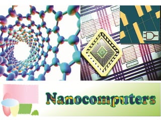
Nanocomputers
- 1. 1
- 2. A nanocomputer is a computer whose physical dimensions are microscopic. The field of nanocomputing is part of the emerging field of nanotechnology . Several types of nanocomputers have been suggested or proposed by researchers and futurists. 2
- 3. Nanotechnology is all about building things atom by atom & molecule by molecule. Goal of this technology is to make tiny devices called ‘Nanomachines’. When manufacturing products made from an atom, the property of those products depends on how those atoms are arranged. 3
- 4. Electronic Nanocomputers Chemical & Bio-Chemical Nanocomputers Mechanical Nanocomputers Quantum Nanocomputers 4
- 5. Electronic nanocomputers would operate in a manner similar to the way present-day microcomputers work. The main difference is the physical scale. To further decrease the size the concept, “Nanolithography” will be needed. Nanolithography is the study and application of a number of techniques for creating nanometer-scale structures, meaning patterns with at least one lateral dimension between the size of an individual atom. (approximately 100 nm) 5
- 6. Chemical and biochemical computers would store and process information in terms of chemical structures and interactions. Biochemical Nanocomputers seems far off because the mechanisms for animal brains are not properly understood by human. In general terms, chemical computer is one that process information in terms of making and breaking chemical bonds & store resulting information in terms of chemical struture. 6
- 7. Tiny Machines & computers would be assembled by the Mechanical Positioning of atoms or molecular building blocks, one atom or molecule at a time. This process is known as “mechanosysthesis”. Mechanical Nanocomputers would use tiny moving components called Nanogears to encode information. Once assembled, the nano computer would operate a bit like the complex programmable version of mechanical calculator. 7
- 8. A Quantum Nanocomputer would work by storing data in the form of atomic quantum states or spin. Technology of this kind is already under development in the form of single-electron memory (SEM) and quantum dots. An electron can easily fall to a lower energy state, emitting a photon; conversely, a photon striking an atom can cause one of its electrons to jump to a higher energy state. Instantaneous electron energy states are difficult to predict and even more difficult to control. 8
- 9. To make ever smaller computing components. To understand computing under uncertainty and with faults. To model and analyze non-deterministic assembly. To cope with faults. To communicate with physical nanotechnologists. 9
- 10. In 1965, engineer Gordon Moore predicted that the number of transistors on an integrated circuit would double approximately every two years. Today, we call this prediction Moore's Law, though it's not really a scientific law at all. Microprocessor manufacturers strive to meet the prediction, because if they don't, their competitors will. 10
- 11. (No. of transistors) 11
- 12. Depending on what it's made from, a nanowire can have the properties of an insulator, a semiconductor or a metal. By arranging semiconductor wires in the proper configuration, engineers can create transistors, which either acts as a switch or an amplifier. Some interesting and counterintuitive properties nanowires possess are due to the small scale. 12
- 13. normally an electron can't pass through an insulator. If the insulator is thin enough, though, the electron can pass from one side of the insulator to the other. It's called electron tunneling. Another interesting property is that some nanowires are ballistic conductors. This means electrons can travel through the conductor without collisions. So, nanowires can conduct electricity efficiently without the byproduct of intense heat. 13
- 14. There are two different approaches to building things in the nanoscale. They are: Although we can build Nanowires using either approach, no one has found a way to make mass production feasible. 14
- 15. The small scales make it very difficult to build transistors automatically right now, engineers usually manipulate wires into place with tools while observing everything through a powerful microscope. 15
- 16. Top-down approach In the way of scientists making fiber-optic nanowires, they use this method. Fiber-optic wires carry information in the form of light. Bottom-up approach Chemical vapor deposition (CVD) is an example of a bottom up method. In general, CVD refers to a group of processes where solids form out of a gaseous phase. 16
- 17. Assembly of a nanoscale computing machine encompasses all the key elements and challenges required to implement the bottom up paradigm. Building blocks of nanocomputers are Nanowires. Nanowires can be synthesized predictably with different chemical compositions and dopants. 17
- 18. Nanowires serve a dual purpose. Both active devices and interconnections. For an example, crossed nanowires can be configured as field effect transistors (FET’s) which amplify signals and can perform logic. 18
- 19. As the gate voltage is changed, conductance increases or decreases between source and drain. Gate Source Drain 19
- 20. The crossed nanowire devices can serve as the basis for universal nanococmputing system built from nanowire arrays which provide memory and logic function, that are interconnected to the outside world using conventional metal lines. 20
- 21. Fluidic or pressure directed assembly is combined with chemical patterning of a substrate to organize nanowire arrays in larger scale. Nanowires in a monolayer of surfactant at the air- water interface. Fluidic Area 21
- 22. These nanowires are transferred into centimeter scale substrates and hierarchically patterend into periodic arrays using photolithography. 22
- 23. In this way, dense crossed nanowire arrays can be patterened with control of all key parameters in a scalable manner over large areas. 23
- 24. A universal architecture for nanoscale computing will require large and dense arrays combining logic, memory and decoding functions. These all can achieveable using nanowires. 24
- 25. Programmable molecules (PMs) at nanowire crosspoints. Nanowires form contacts groups at ohmic contacts (OCs). Nanowire and Mesowire junctions form FETs. Nanowires controlled by meso scale wires (MWs). Dense memories (1011 bits/cm2) and circuits predicted. 25
- 26. Crossbars can serve as a basis for both memories and circuits. Semiconductor nanowires (NWs) can be stochastically assembled into crossbars NW-based crossbars must interface with lithographically produced technology. Decoders provide an efficient defect-tolerant interface. 26
- 27. Electrostatic attraction used to make contacts, repulsion breaks them. Permanently nonvolatile memory Speed comparable to DRAM/SRAM Density comparable to DRAM Unlimited lifetime Immune to soft errors 27
- 28. The company Apple has released an experimental device called Nanocomputer iLens that aims to facilitate and improve vision of the human being. This Bionic contact lens has photographic memory, binoculars, night vision and augmented reality with a heads up display. Running with the basic functions of a computer, this is why Apple research team called it a nanocomputer. There is still a lot to develop in this app. 28
- 29. Here is the type of vision you can get using these lenses. 29
- 30. 30