SlideShare uma empresa Scribd logo
1 de 11
Baixar para ler offline
'l
USN
Time: 3 hrs.
Notet Answer FIVE full questions, selecting
at least TWO questions from each part.
06EC7t
Max. Marks:100
of addresses that are used in an
(t0 Marks)
(06 Marks)
(10 Marks)
(06 Marks)
(04 Marks)
Seventh Semester B.E. Degree Examination, June/July 2013
Gomputer Gommunication Networks
s
.b
3c
6q)
.=.l
.=.9
e..
d=
.>
-i .i
o
z
E
PART - A
I a. Explain briefly with relevant examples, the four levels
2a.
b.
c.
3a.
4 a. List the goals offast Ethernet.
internet employing the TCP/IP protocols. (10 Marks)
b. Briefly describe the functions ofphysical layer and data link layer. (06 Marks)
c. Explain the operation of ADSL using 'Discrete Multitone Technique' indicating the
different chaanels, with a diagram. (04 Marks)
Explain the mechanism of selective repeat ARQ with diagram showing send window and
receive window (10 Marks)
With suitable block diagram, explain the stop and wait protocol, for noise less channels.
Also write the sender site algorithm. (06 Marks)
Perform bit stufling and unstuffing on the given bit stream: 0001111111001111101000.
Assume 11ag as 01 1 1 1 I 10. (04 Marks)
Explain how collisions are avoided through use of 'lFS, contention window and
acknowledgments' in CSMA,/CA. With the help of the flow chart show the procedure for
CSMA/CA.
b. Explain'Token Passing' method ofcontrolled access ofthe channel.
c. A slotted ALOHA network transmit 200 bit frames using a shared channel with a 200 kbps
bandu,idth. Find the throughput if the system produces i) 1000 frames per second
ii) 500 frames per second iii) 250 frames per second. (04 Marks)
5a.
Explain the features ofphysical layer in fast Ethernet.
b. Explain two different kinds of serr,,ices as defined in IEEE 802. I 1.
c. Write a note on Piconet and Scatternet in Bluetooth.
PART - B
A sysiem with four LANs and frv"-G@ rhown in Fig.Qs(a). Choose Bl as the root
bridge. Show the fbrwarding and blocking ports, after applying the spanning tree procedure.
LeF,+
Fig.Qs(a)
1of2
LhNI
(10 Marks)
t
,
l
06EC71
b. Define repeater, bridge and router with necessary diagrams' (06 Marks)
c. Differentiate between a bus backbone network and star backbone network. (04 Marks)
. 6 a. An ISP is granted a block of addresses starting with 150.80.0.0/16. The ISP wants to
-' distribute these blocks of2600 customers as follows:
D The first group has 200 medium size business; each needs 16 addresses'
ii) The second group has 400 small business; each needs 8 addresses'
iii) The third grJup has 2000 households; each needs 4 addresses'
,' Design the subblocks and give the slash notation for each subblock. Find out how many
adtltesses ate still available after these allocations. (10 Marks)
b. eiplain briefly strategies used to handle the transition from IPv4 to IPv6. (06 Marks)
c. A
'blbii;.of
addressis is granted to a small organization. One of the addresses is
205.16.37.39128. What is the first address, last address and number of address in the block.
7a. Explain the 'Distarfe Vector Routing' 'for the following e1mple shown in Fig.Q7(a)'
(10 Marks)
(04 Marks)
Briefly discuss the foltowing forwarding techniques:
i) Next-Hop method versus Route method
ii) Network-specific method versus Host specific method.
Distinguish between diulticasting and multiple unicasting.
Explain connection establishment and connection termination,in TCP. (10 Marks)
write a note on DNS. (06 Marks)
Write a shorri irote on source port number and destination port nurnber.in user datagram.
' (04 Marks)
(06 Marks)
(04 Marks)
8a.
b.
c.
Fig.Q7(a)
2 of2
r
USN
Time: 3 hrs.
068C72
Max. Marks:100
(06 Marks)
(06 Marks)
of glass fiber, how RI can be
(04 Marks)
approximately 1000 modes at an 850nm
Seventh Semester B.E. Degree Examination, June/July 2013
Optical Fiber Gommunication
Note: Answer FIVEfull questions, selecting
at leost TWO questions from each part.
o
E
I
ai!
'=^
a-a
o."
,i .9
6,
at=
o ::
6.S
o<
.i ..i
o
z
E
la.
b.
c.
PART-A
Discuss the advantages and disadvantages ofOFC.
Explain Mode Field Diameter (MFD) of a single mode fiber.
Differentiate between glass fiber and plastic fibers. In case
varied?
d. A SI multimode fiber with a NA of 0.20 supports
wavelength.
i) What is the diameter of its core?
iD How many modes does the fiber support at
iii) How many modes does the fiber support at
2 a. Explain the "pulse dispersion" with suitable diagram and ditferentiate MMSIF, MMGIF and
SMF by their information carrying capacity with reason. (06 Marks)
b. Discuss the following for optical fibers:
i) Extrinsicabsorprion.
ii) Materialdispersion.
c. Optical power launched into fiber at transmitter end is 150pw. The power at the end of
10km length of the link working in first window is -38.2 dBm. Another s/m of same length
working in second window is 47.5 pw. Same length sim working in third window has 50%
of launched power. Calculate ltber attenuation for each case and mention wavelength of
operation. (06 Marks)
3 a. A double-hetero junction "lnGaAsP" LED emitting at a peak,wavelength of 1310 nm has
radiative and non radiative recombination times of 25 ns and 90 ns respectively. The drive
current is 35 mA.
i) Find the internal quantum efficiency and the internal power.
ii) If the RI of the light source material is n : J.5. Find the power emitted iiom the
device. (06 Marks)
b. Describe the following terms relating to LASER:
i) External quantum efficiency.
ii) Wavelengthspacing.
c. Explain the tlree lactors which affects the response time ofa photodiode.
4 a- Discuss the different lensing scheme used to improve the source-to-fiber coupling
efficiency, with the necessary sketches. (06 Marks)
b. For a surface emitting LED has radiance of l50W(cm2.sr) and radius of emitting area is
35pm. Calculate the optical power coupled to the fibers with
1320 nm?
1550 nm? (04 Marks)
(08 Marks)
(06 Marks)
(08 Marks)
(06 Marks)
(08 Marks)
a1 = 25prm and NA : 0.20, step index
a2 : 50pm and N A:0.20, step index.
c. Define fiber splicing. Explain different types of splicing with neat sketches.
1 of2
t-I

06F,C72
PART-B
5 a. Explain the different tlpes of front-end amplifiers in optical receiver. (06 Marks)
b. With a neat sketch, explain how system performance information can be obtained from the
eye diagram.
c. Write a short note on burst-mode receivers.
(08 Marks)
(06 Marks)
-.':g a. Following are the parameters of a point-to-point optical link:
:- - i) Optical power launched : +3dBm
,. il) Sensitivity ofdetector : -32dBm
r'- iii) Source/detector connector loss : 1dB
'iv), Length ofoptical cable : 60 km
v1'...
t'Cable attenuation : 0.3dB/kmv1'...t'Cable attenuation : 0.3dB/km
vi) ' Jqrnper cable loss : 3dB
vii) Co'nnector loss at each fiber :1dBLbnnector loss at eacn rlDer : lol]' r-'
joint (two at each transmitter and receiver
end be&trse of the jumper cables)
Compute the powel margin of the link using spread sheet'mbthod' (06 Marks)
b. Explain the basic eleruents of analog link with differenl nrii3e contribution. (09 Marks)
c. What is sub carrier multiplexing? Explain. (05 Marks)
7 a. Explain the need of isolator iiidptical network.'Give its principle of operation also.
(06 Marks)
f. Explain the operational principle an! iilplementation of WDM. (08 Marks)
s. Briefly discuss dielectric thin-film ftltg1C;. (06 Marks)
,'-- I
'.,
8 a. Explain the three main optical amplifier types. (06 Marks)
b. Describe:
i) SONET/SDH rings..,.
ii) SONET/SDHnetworks.
iii) Frame format pf STS-1 SONET. (t0 Marks)
c. An EDFA amplifier'produces P..out : 27dBm for an input Pqio = 2dBm at 1542 nm.
i) Find the aipplifier gai4 G.
ii)
Y,i:
*" minimum pump power required. (04 Marks)
.-. ,;..i * * * :t *
2 of2
I
USN 06EC73
(12 Marks)
(02 Marks)
(10 Marks)
(06 Marks)
E
89
te
bE
-a'CA
tq
,i .?
a,i
6.Y
a3
9<
- ..i
o
z
o
F
Seventh Semester B.E. Degree Examination, June / July 2013
Power Electronics
Time: 3 hrs. Max. Marks:100
Note: l. Answer any FIVE full questions, selecting
utleost TWO question from each part.
2. Draw neat diagram and Waveforms, wherever possible.
P.{RT - A
I a. What is Power Electronics? Draw a neat block diagram of generalized power converter
system. State the applications ofpower dlectronics. (06 Marks)
b. With neat circuit diagram and waveforms. explain the rypes of power electronjc circuils.
2 a. The maximum junction temperature of a transistor is Tt : 1500C and the ambient
temperature is To:250a, If the thermal impedances are &c:0.40ClW, R.,:0.1oC/W, and
Rse : 0.50C/W. Calculate i) the maximum power dissipation and ii) the case
c. Compare General purpose, Fast recovery and Schokky diodes.
n - tlpe (enhancement) MOSFET.
c. Write a note on isolation ofgate and base drives.
temperature. (0,1 Marks)
b. With the help of parasitic model and switching model, explain the switching waveforms of
3 a. Using a two transistor model of thyistor, show that Ie =
olq +
]tuu' * Iquo'
. (06 Marks)
1 - (cr, +crr)
b. With neat sketch, explain turn on characteristics of SCR. (06 Marks)
c. The input voltage Fig. Q3(c) is V, = 200V with load resistance of R - 5O. The load and
stray inductances are negligible and the thy,ristor is operated at a frequency of f. : 2KHz. If
the required dv/dt is 100 V/pS and the discharge current is limited to 100,4.. Determine i)
the values ofR. and C. ii) the snubber loss, and iii) the power rating of the snubber
resistor. (08 Marks)
Pi3 . q3 c.d"/dv Y*u.-..t.,,,.,
C.,r.cliL
4a.
b.
c.
Discuss the effect of inductance using the 1 - O full converter. (08 Marks)
What is phase control? Explain the principal of phase control using 1 - $ half wave
controlled rectifier. (08 Marks)
Compare circulating and non - circulating mode ofoperation ofdual converter. (04 Marks)
1 of 2
I
b.
06EC73
PART-B
A thyistor circuit is shown in fig. Q5(a), if thyristor Tr is switched on at t: 0, determine
the conduction time of thyristor Tr and the capacitor voltage after Tr is tumed off. The
circuit parameters are L : l0pH, C - 50pF and V' - 200V. The inductor carries an iniiial
current oflm = 250A. (10 Marks)
e Pl5 , 4.5a : o"t5 c..,r-*t^ u.J
a.r. c- i t_
is ihe principle of complementary commutation? Explain the same with the help of
suitable circuit and waveforms. (10 Marks)
What is the principle of on off control? Explain the sanie r,nith a single phase full - wave
controller. (06 Marks)
Draw a neat sketch of 1 - $ AC voltage controller with RL load and explain its working.
(06 Marks)
c. A single - phase full wave AC voltage controller has a resistive load of R: l0 O and the
input voltage is V.: 120V (rms), 60H2. The delay angles of thyristors Tr and T2 ilre eQual
ol : 02: r/2. Determine i) the rms output voltage V" ii) the input power factor PF
iii) the average current ofth},ristor Inand iv) the rms current ofthlaistor IR. (08 Marks)
With a neat circuit diagram, explain the operation of a step down chopper and also explain
constant frequency and variable frequency operation. Derive an expression for output
voltage incase ofstep down chopper. (10 Marks)
b. A step - up chopper with a pulse width of200ps operating on 200V, dc supply. Calcualte
the output voltage, ifthe blocking period ofthe device is 50ps. (02 Marks)
c- With a neat and quadrant operation, explain class E chopper. (08 Marks)
a. With a neat circuit diagram, of 1 - { half bridge inverter, explain the principle of operation
ofan inverter. (08 Marks)
b. write briefnote on current source inverter. , (06 Marks)
c. With the help of circuit diagram and waveforms, explain a variable DC -,trO t"u.[?.nnurur,
2 of2
USN 068C74
TMS320C54XX
(10 Marks)
either on-chip or
(06 Marks)
located in
(04 Marks)
Seventh Semester B.E. Degree Examination, June/Juty 2013
c.
d.
g
I
te
:q
56
9JE
G- tq
r--) <
-i ..i
a
z
A
E
DSP Algorithms and Architecture
Time: 3 hrs. Max. Marks:100
Note: Answer FIVE fult questions, selecting
at least TWO questions from each part.
PART_A
I a' List and explain the issues that have to considered in designing and implementing a DSp
system. (04 Marks)
[. lmplement an FIR firter ror y(n)-
(xtn)+x(n
-l)+xtn-2)). Determine the (i) sysrem
function (ii) magnitude response function (iii) phase response function. Plot its magnitude
and phase response. (06 Marks)
c. Explain the process of decimation. (04 Marks)
d The signal sequence x(n) : [0 2 4 6 Sl is interpolated using the interpolation filter
sequence h : [0.5 1 0.5] and the interpolation factor is 2. Deiermine thi interpolated
sequence y(m). (06 Marks)
b.
Explain the different frequently used teohniqries to prevent overflow and underflow
conditions occuning in MAC unit. (04 Marks)
Explain the diftbrent ways in which the on-chip memory can be organized efficiently and
cost-effective manner. (04 Marks)
Explain the register pointer updating algorithm for circular buffer addressing mode.
(04 Marks)
I-.ist the techniques used in DSP architecture to increase speed of operation and operations
that should be accomplished in single clock to achieve purull.li.- in DSp iomplementation.
(08 Marks)
Explain with a neat clock diagram the indirect addressing mode of
processor. Give the operand syntax and operation for the followins:
i) Circular addressing mode ii) Bit reverse addressing mode.
Ex-plain the different ways in which PC addresses the program memory
off-chip and gets loaded for execution ofinstructions.
Specifl the on-chip memory configurarion lor Mpl MC, OVLy and DROM
processor mode status register of 5416 processor.
Describe the operation and application of the following instructions of rMS320c54XX
processor with example:
i,) MAC i, MAS iii) LD *AR4,4, A
Given contents ofAR4 is 8boeh& SxM: l. Determine the contents ofaccumulator.
(06 ,larks)
Write an ALP of TMS320C54XX processor to compute
{n) = h cos x(n) + h(1) x(n - l) + h(2) x(n - 2), using MAC instruction, where h(0) : 5,
h(l) : 31, h(2) : 13 are in program memory loiations starting at tr. 4n)
'=
t,
x(n- 1):5 x(n - 2)= -3 are in data memory locations starting at iy(n) is to be saved
(lo.wer 16 bits) in location y and y +l (higher 16 bits). (0s Marks)
With a neat sketch, describe the Host port interface signals. 1Or tr.lart<g
Explain the six-stage pipelined execution of TMS320C54XX. .i , , ios tuartg
I of 2
3a.
b.
c.
4a.
b.
c.
d.
a program for a second order IIR filter on TMS320C54XX processor
defined by the transfer function H(z) - 0.104 - 0.1022-1 + 0.1042-2
Assume that the filter
1+ z-t - 0.6122-2
poefficients are qls numbers x(n) is the input sample (integer), input samples. are placed in
i tnrffer, insamples, fiom a data file, data-in.dat. y(n) is computed output. The output samples
ard placed in a buffer outsamples. (10 Marks)
c. Explain-with necessary block diagram, memory organization for implementing FIR filter of
orderN.-'.. (05 Marks)
6 a. Determine the following for a 512 point FFT computation :
i) Number of stages ii) Number of butterflies in each stage iii) Number of butterflies
needed [or the entire computation. iv) Number ol butterllies that need no twiddle lactors.
v) Number of butterflies ttial require real twiddle factors vi) Number of butterflies that
require complex twiddle factors. (06 Marks)
b. Explain how scaling prevents overflow conditions in the butterfly computation. (06 Marks)
c. Write a TMS320C54XX program'segment that implements 8 point DIT FFT bit reversed
PART _ B
Explain Q7 and Qrs Notations with example.
068C74
(05 Marks)
(08 Marks)
DSP in the address range
(06 Marks)
IIO ND
(06 Marks)
(08 Marks)
(06 Marks)
(O8 Marks)
5 a. Define Q Notation.
b. Realize and write
index generation and to clear FFT dlrta memory.
'...''
7 a. Interface an 8kx 16 prqsaril ROM to the C5416
TFEOOOh _ TFFFFFh.
b. Explain with a flow''chdrt diagram for software polling for the programmed
converter interface.
c. Define intemrpt. Write a flow chart of interrupt handling by C54XX processor.
8 a. Explafuriith neat block diagram the PCM 3002 interfaced to TMS320VC5416 in the DSK.
(06 Marks)
b. .Explain with block diagram the biotelemetry receiver implementation.
i.. 'With a neat sketch, explain the JPEG encoder and decoder.
*****
2 of2
/
USN
PART - B
WIy smoothing is needed in image processing? What is
ideal LPF and Butterworlh LPF in the above context.
accomplish this.
06EC756
its effect on the image? ExPlain an
(10 Marks)
to transform the
in Fig.Qs(b)(ii).
and z that will
(10 Marks)
I
o
o
g@
;g
o'o
i: _:
-9=
9<
Z
o
E
Seventh Semester B.E. Degree Examination, June/July 2013
lmage Processing
Time: 3 hrs. Max. Marks:100
Note': Answer FIVEfull questions, selecting
at least TWO questions from each parl
PART - A
I a. with a neat block diagram explain the fundamental steps in digital processing. (10 Marks)
b. Consider the two image subsiates Sr and Sz shown in Fig.Ql(b). For V: < 1 >, determine
whether these two subsets are: i) 4-adiacent, ii) S-adjacent or (iii) M-adjacent. (10 Marks)
S1 S2
D
I
I
o
O l ll Ao ll l
Fig.Ql(b)
2 a. Explain the role of sampling and Quantization in image processing system' (10 Marks)
b. what are the basic relationships between pixels? with neat diagrams and appropriate
mathematical expressions, explain (i) neighbours, ii) adjacency, iii) connectivity. (t0 Marks)
3 a. With respect to 2D discrete Fourier transform of an image, explain the following, derive
suitable equations:
i) Separability ii) Transition iii) Rotalion iv) Periodicity (10 Marks)
b. Explain the homomorphic filtering approach fbr image enhancement (10 Marks)
4 a. Give the expression for Hadamord transform and generate the corresponding 1-D Kernal for
N :4. Explain any two ofits properties. (12 Marks)
b. Write an explanatory note on Histogram equalization. (08 Marks)
5a.
b. An image has the gray level pdf p(r) shown in Fig.Q5(b)(i). It is desired
gray levels of this images so that they will have the specified p(z) shown
Assume continuous quantities and find the transformation in terms of r
? Lz)
ootl
oloo
rtDo
o ao o
o o oo
oo
oolo
otll
Pie.Qs(b)(i)
1of2
6 a. With the help of a neat graphical illustration, explain the powerJaw
piecewise linear contrast stretch.
b. Explain how image degradation is carried out using:
06EC7s6
transformation and
(10 Marks)
(10 Marks)
(10 Marks)
(10 Marks)
, r'.'
.'.':.]
-.
r 1"..1i_
.-..i. t
2 of2
T]SN
Seventh Semester B.E. Degree Examination, June/July 2013
-s
--t
dql]
0r i;
i. (E
do
6'=
o- ;i
ca
-i c.i
o
z
E
1a.
b.
4 a. Explain scope and visibility of a variable.
b. What are the basic language requirements for RT language? Explain.
c. What is CUTLASS? What are the requfuements of CUTLASS?
PART - B
5 a. Explain dilTerent scheduling strategies.
b. Three cyclic tasks A, B, C are required to run at 1 tick, 2 ticks and
(1 tick : 20 ms). Assuming tasks A, B, C consumes 5 ms, 8 ms and
Write task activation diagram lor priority order. (Context switching time
i) A (highest), B, C ii) B (highest), A, C
c. What is code sharing? Explain serially reusable and re-entrant code.
Real Time Systems
Time: 3 hrs.
Notez Answer FIVE full questions, selecting
dt least TWO questions from each part'
PART-A
Give two definitions for real time system.
Explain dilferent classifications ol RTS based on synclronization
6 a. With a neat diagram, explain the general structure of IOSS.
b. Explain the problem of shared memory. How semaphores are
problem?
c. Explain Liveness.
a. Explain foreground and background system with a flowchart.
b. Differentiate pool and channel.
c. Explain software design for RTS using software module.
a. Explain lunctional specifications with respect to a drying oven.
b. Explain Yourdon methodologY.
c. With a relevant diagram, explain Ward and Mellor's method'
and intemal tasks ofthe comPuter.
c. Explain hard and soft RTS with relevant equations.
2 a. Compare batch processing and continuous processing
b. With a neat diagram, explain distributed systems with its advantages.
c. Write a note on supervisory control systems.
3 a. The clock on computer generates an interrupt for every 20 ms' Draw a flow chart for
interrupt service routine, *hi.h hu, to keep a 24 hour clock in terms of hours, minutes and
seconds' (08 Marks)
b. Explain a simple digital input and output interiaces. (10 Marks)
c. Write a note on different LAN topologies. (02 Marks)
o6EC762
Max. Marks:100
(04 Marks)
between external process
(08 Marks)
(08 Marks)
(05 Marks)
(10 Marks)
(05 Marks)
(04 Marks)
(10 Marks)
(06 Marks)
(06 Marks)
3 ticks respectively
10 ms respectively.
: 0).
(06 Marks)
(08 Marks)
(07 Marks)
used to overcome this
(09 Marks)
(04 Marks)
(10 Marks)
(04 Marks)
(06 Marks)
(07 Marks)
(05 Marks)
(08 Marks).

Mais conteúdo relacionado

Mais procurados

physics-chapter-4-form-5
 physics-chapter-4-form-5 physics-chapter-4-form-5
physics-chapter-4-form-5
AinHaini
 
Electronics module
Electronics moduleElectronics module
Electronics module
Ota Keiko
 
E L E C T R I C A L C I R C U I T S A N A L Y S I S J N T U M O D E L P ...
E L E C T R I C A L  C I R C U I T S  A N A L Y S I S  J N T U  M O D E L  P ...E L E C T R I C A L  C I R C U I T S  A N A L Y S I S  J N T U  M O D E L  P ...
E L E C T R I C A L C I R C U I T S A N A L Y S I S J N T U M O D E L P ...
guest3f9c6b
 
E L E C T R O M A G N E T I C W A V E S A N D T R A N S M I S S I O N L I N E...
E L E C T R O M A G N E T I C W A V E S A N D T R A N S M I S S I O N L I N E...E L E C T R O M A G N E T I C W A V E S A N D T R A N S M I S S I O N L I N E...
E L E C T R O M A G N E T I C W A V E S A N D T R A N S M I S S I O N L I N E...
guest3f9c6b
 
See 2523 sze 2523 2
See 2523 sze 2523 2See 2523 sze 2523 2
See 2523 sze 2523 2
frazatas
 

Mais procurados (12)

physics-chapter-4-form-5
 physics-chapter-4-form-5 physics-chapter-4-form-5
physics-chapter-4-form-5
 
Electronics module
Electronics moduleElectronics module
Electronics module
 
E L E C T R I C A L C I R C U I T S A N A L Y S I S J N T U M O D E L P ...
E L E C T R I C A L  C I R C U I T S  A N A L Y S I S  J N T U  M O D E L  P ...E L E C T R I C A L  C I R C U I T S  A N A L Y S I S  J N T U  M O D E L  P ...
E L E C T R I C A L C I R C U I T S A N A L Y S I S J N T U M O D E L P ...
 
E L E C T R O M A G N E T I C W A V E S A N D T R A N S M I S S I O N L I N E...
E L E C T R O M A G N E T I C W A V E S A N D T R A N S M I S S I O N L I N E...E L E C T R O M A G N E T I C W A V E S A N D T R A N S M I S S I O N L I N E...
E L E C T R O M A G N E T I C W A V E S A N D T R A N S M I S S I O N L I N E...
 
A109210204 electrical-circuits1
A109210204 electrical-circuits1A109210204 electrical-circuits1
A109210204 electrical-circuits1
 
See 2523 sze 2523 2
See 2523 sze 2523 2See 2523 sze 2523 2
See 2523 sze 2523 2
 
17472 principal of comm system
17472  principal of comm system17472  principal of comm system
17472 principal of comm system
 
R05010204 E L E C T R O N I C D E V I C E S A N D C I R C U I T S
R05010204  E L E C T R O N I C  D E V I C E S  A N D  C I R C U I T SR05010204  E L E C T R O N I C  D E V I C E S  A N D  C I R C U I T S
R05010204 E L E C T R O N I C D E V I C E S A N D C I R C U I T S
 
11903 Electromagnetic Waves And Transmission Lines
11903 Electromagnetic Waves And Transmission Lines11903 Electromagnetic Waves And Transmission Lines
11903 Electromagnetic Waves And Transmission Lines
 
Hvdc Transmission Jntu Model Paper{Www.Studentyogi.Com}
Hvdc Transmission Jntu Model Paper{Www.Studentyogi.Com}Hvdc Transmission Jntu Model Paper{Www.Studentyogi.Com}
Hvdc Transmission Jntu Model Paper{Www.Studentyogi.Com}
 
17439 principal of analog communication
17439  principal of analog communication17439  principal of analog communication
17439 principal of analog communication
 
Performance analysis of transmission of 5 users based on model b using gf (5)...
Performance analysis of transmission of 5 users based on model b using gf (5)...Performance analysis of transmission of 5 users based on model b using gf (5)...
Performance analysis of transmission of 5 users based on model b using gf (5)...
 

Semelhante a 7th Semester Electronic and Communication Engineering (2013-June) Question Papers

Semelhante a 7th Semester Electronic and Communication Engineering (2013-June) Question Papers (20)

7th Semeste Electronics and Communication Engineering (June-2016) Question Pa...
7th Semeste Electronics and Communication Engineering (June-2016) Question Pa...7th Semeste Electronics and Communication Engineering (June-2016) Question Pa...
7th Semeste Electronics and Communication Engineering (June-2016) Question Pa...
 
7th Semeste Electronics and Communication Engineering (June-2016) Question Pa...
7th Semeste Electronics and Communication Engineering (June-2016) Question Pa...7th Semeste Electronics and Communication Engineering (June-2016) Question Pa...
7th Semeste Electronics and Communication Engineering (June-2016) Question Pa...
 
2nd Semester M Tech: VLSI Design and Embedded System (June-2016) Question Papers
2nd Semester M Tech: VLSI Design and Embedded System (June-2016) Question Papers2nd Semester M Tech: VLSI Design and Embedded System (June-2016) Question Papers
2nd Semester M Tech: VLSI Design and Embedded System (June-2016) Question Papers
 
6th Semeste Electronics and Communication Engineering (June-2016) Question Pa...
6th Semeste Electronics and Communication Engineering (June-2016) Question Pa...6th Semeste Electronics and Communication Engineering (June-2016) Question Pa...
6th Semeste Electronics and Communication Engineering (June-2016) Question Pa...
 
7th Semester (June; July-2014) Electronics and Communication Engineering Ques...
7th Semester (June; July-2014) Electronics and Communication Engineering Ques...7th Semester (June; July-2014) Electronics and Communication Engineering Ques...
7th Semester (June; July-2014) Electronics and Communication Engineering Ques...
 
8th Semester Electronic and Communication Engineering (2013-June) Question Pa...
8th Semester Electronic and Communication Engineering (2013-June) Question Pa...8th Semester Electronic and Communication Engineering (2013-June) Question Pa...
8th Semester Electronic and Communication Engineering (2013-June) Question Pa...
 
6th Semester Electronic and Communication Engineering (2013-December) Questio...
6th Semester Electronic and Communication Engineering (2013-December) Questio...6th Semester Electronic and Communication Engineering (2013-December) Questio...
6th Semester Electronic and Communication Engineering (2013-December) Questio...
 
3rd Semester M Tech CMOS VLSI Design (Dec-2013) Question Papers
3rd Semester M Tech CMOS VLSI Design (Dec-2013) Question Papers3rd Semester M Tech CMOS VLSI Design (Dec-2013) Question Papers
3rd Semester M Tech CMOS VLSI Design (Dec-2013) Question Papers
 
8th Semester (Dec-2013) Electronic and Communication Engineering Question Pap...
8th Semester (Dec-2013) Electronic and Communication Engineering Question Pap...8th Semester (Dec-2013) Electronic and Communication Engineering Question Pap...
8th Semester (Dec-2013) Electronic and Communication Engineering Question Pap...
 
8th Semester (June; July-2014) Electronics and Communication Engineering Ques...
8th Semester (June; July-2014) Electronics and Communication Engineering Ques...8th Semester (June; July-2014) Electronics and Communication Engineering Ques...
8th Semester (June; July-2014) Electronics and Communication Engineering Ques...
 
6th Semeste Electronics and Communication Engineering (Dec-2015; Jan-2016) Qu...
6th Semeste Electronics and Communication Engineering (Dec-2015; Jan-2016) Qu...6th Semeste Electronics and Communication Engineering (Dec-2015; Jan-2016) Qu...
6th Semeste Electronics and Communication Engineering (Dec-2015; Jan-2016) Qu...
 
1st and 2nd Semester 2018 scheme C cycle model question papers
1st and 2nd Semester 2018 scheme C cycle model question papers1st and 2nd Semester 2018 scheme C cycle model question papers
1st and 2nd Semester 2018 scheme C cycle model question papers
 
7th Semester Electronics and Communication Engineering (Dec-2015; Jan-2016) Q...
7th Semester Electronics and Communication Engineering (Dec-2015; Jan-2016) Q...7th Semester Electronics and Communication Engineering (Dec-2015; Jan-2016) Q...
7th Semester Electronics and Communication Engineering (Dec-2015; Jan-2016) Q...
 
6th Semester Electronic and Communication Engineering (2013-June) Question Pa...
6th Semester Electronic and Communication Engineering (2013-June) Question Pa...6th Semester Electronic and Communication Engineering (2013-June) Question Pa...
6th Semester Electronic and Communication Engineering (2013-June) Question Pa...
 
6th Semester Electronic and Communication Engineering (June/July-2015) Questi...
6th Semester Electronic and Communication Engineering (June/July-2015) Questi...6th Semester Electronic and Communication Engineering (June/July-2015) Questi...
6th Semester Electronic and Communication Engineering (June/July-2015) Questi...
 
6th Semester (June; July-2014) Electronics and Communication Engineering Ques...
6th Semester (June; July-2014) Electronics and Communication Engineering Ques...6th Semester (June; July-2014) Electronics and Communication Engineering Ques...
6th Semester (June; July-2014) Electronics and Communication Engineering Ques...
 
8th Semeste Electronics and Communication Engineering (June-2016) Question Pa...
8th Semeste Electronics and Communication Engineering (June-2016) Question Pa...8th Semeste Electronics and Communication Engineering (June-2016) Question Pa...
8th Semeste Electronics and Communication Engineering (June-2016) Question Pa...
 
2nd Semester M Tech: Computer Science and Engineering (Jun-2016) Question Pa...
2nd  Semester M Tech: Computer Science and Engineering (Jun-2016) Question Pa...2nd  Semester M Tech: Computer Science and Engineering (Jun-2016) Question Pa...
2nd Semester M Tech: Computer Science and Engineering (Jun-2016) Question Pa...
 
1st Semester M Tech Computer Science and Engg (Dec-2013) Question Papers
1st Semester M Tech Computer Science and Engg  (Dec-2013) Question Papers 1st Semester M Tech Computer Science and Engg  (Dec-2013) Question Papers
1st Semester M Tech Computer Science and Engg (Dec-2013) Question Papers
 

Mais de BGS Institute of Technology, Adichunchanagiri University (ACU)

Mais de BGS Institute of Technology, Adichunchanagiri University (ACU) (20)

4th Semester Computer Science and Engineering (ACU-2022) Question Paper
4th Semester Computer Science and Engineering (ACU-2022) Question Paper4th Semester Computer Science and Engineering (ACU-2022) Question Paper
4th Semester Computer Science and Engineering (ACU-2022) Question Paper
 
3rd Semester Computer Science and Engineering (ACU - 2022) Question papers
3rd Semester Computer Science and Engineering  (ACU - 2022) Question papers3rd Semester Computer Science and Engineering  (ACU - 2022) Question papers
3rd Semester Computer Science and Engineering (ACU - 2022) Question papers
 
3rd Semester Computer Science and Engineering (ACU - 2021) Question papers
3rd Semester Computer Science and Engineering  (ACU - 2021) Question papers3rd Semester Computer Science and Engineering  (ACU - 2021) Question papers
3rd Semester Computer Science and Engineering (ACU - 2021) Question papers
 
3rd Semester Computer Science and Engineering (ACU) Question papers
3rd Semester Computer Science and Engineering  (ACU) Question papers3rd Semester Computer Science and Engineering  (ACU) Question papers
3rd Semester Computer Science and Engineering (ACU) Question papers
 
3rd Semester Computer Science and Engineering (ACU) Question papers
3rd Semester Computer Science and Engineering  (ACU) Question papers3rd Semester Computer Science and Engineering  (ACU) Question papers
3rd Semester Computer Science and Engineering (ACU) Question papers
 
3rd Semester Computer Science and Engineering (ACU) Question papers
3rd Semester Computer Science and Engineering  (ACU) Question papers3rd Semester Computer Science and Engineering  (ACU) Question papers
3rd Semester Computer Science and Engineering (ACU) Question papers
 
3rd Semester Computer Science and Engineering (ACU-2022) Question papers
3rd Semester Computer Science and Engineering  (ACU-2022) Question papers3rd Semester Computer Science and Engineering  (ACU-2022) Question papers
3rd Semester Computer Science and Engineering (ACU-2022) Question papers
 
3rd Semester Computer Science and Engineering (ACU) Question papers
3rd Semester Computer Science and Engineering  (ACU) Question papers3rd Semester Computer Science and Engineering  (ACU) Question papers
3rd Semester Computer Science and Engineering (ACU) Question papers
 
3rd Semester Computer Science and Engineering (ACU) Question papers
3rd Semester Computer Science and Engineering  (ACU) Question papers3rd Semester Computer Science and Engineering  (ACU) Question papers
3rd Semester Computer Science and Engineering (ACU) Question papers
 
8th Semester Civil Engineering Question Papers June/july 2018
8th Semester Civil Engineering Question Papers June/july 20188th Semester Civil Engineering Question Papers June/july 2018
8th Semester Civil Engineering Question Papers June/july 2018
 
7th Semester Civil Engineering Question Papers June/july 2018
7th Semester Civil Engineering Question Papers June/july 20187th Semester Civil Engineering Question Papers June/july 2018
7th Semester Civil Engineering Question Papers June/july 2018
 
6th Semester Civil Engineering Question Papers June/july 2018
6th Semester Civil Engineering Question Papers June/july 20186th Semester Civil Engineering Question Papers June/july 2018
6th Semester Civil Engineering Question Papers June/july 2018
 
5th Semester Civil Engineering Question Papers June/july 2018
5th Semester Civil Engineering Question Papers June/july 20185th Semester Civil Engineering Question Papers June/july 2018
5th Semester Civil Engineering Question Papers June/july 2018
 
4th Semester Civil Engineering Question Papers June/july 2018
4th Semester Civil Engineering Question Papers June/july 20184th Semester Civil Engineering Question Papers June/july 2018
4th Semester Civil Engineering Question Papers June/july 2018
 
3rd Semester Civil Engineering Question Papers June/july 2018
3rd Semester Civil Engineering Question Papers June/july 2018 3rd Semester Civil Engineering Question Papers June/july 2018
3rd Semester Civil Engineering Question Papers June/july 2018
 
8th Semester Mechanical Engineering (June-2016) Question Papers
8th Semester Mechanical Engineering (June-2016) Question Papers8th Semester Mechanical Engineering (June-2016) Question Papers
8th Semester Mechanical Engineering (June-2016) Question Papers
 
7th Semester Mechanical Engineering (June-2016) Question Papers
7th Semester Mechanical Engineering (June-2016) Question Papers7th Semester Mechanical Engineering (June-2016) Question Papers
7th Semester Mechanical Engineering (June-2016) Question Papers
 
6th Semester Mechanical Engineering (June-2016) Question Papers
6th Semester Mechanical Engineering (June-2016) Question Papers6th Semester Mechanical Engineering (June-2016) Question Papers
6th Semester Mechanical Engineering (June-2016) Question Papers
 
5th Semester Mechanical Engineering (June-2016) Question Papers
5th Semester Mechanical Engineering (June-2016) Question Papers5th Semester Mechanical Engineering (June-2016) Question Papers
5th Semester Mechanical Engineering (June-2016) Question Papers
 
4th Semester Mechanical Engineering (June-2016) Question Papers
4th Semester Mechanical Engineering (June-2016) Question Papers4th Semester Mechanical Engineering (June-2016) Question Papers
4th Semester Mechanical Engineering (June-2016) Question Papers
 

Último

Seal of Good Local Governance (SGLG) 2024Final.pptx
Seal of Good Local Governance (SGLG) 2024Final.pptxSeal of Good Local Governance (SGLG) 2024Final.pptx
Seal of Good Local Governance (SGLG) 2024Final.pptx
negromaestrong
 
Beyond the EU: DORA and NIS 2 Directive's Global Impact
Beyond the EU: DORA and NIS 2 Directive's Global ImpactBeyond the EU: DORA and NIS 2 Directive's Global Impact
Beyond the EU: DORA and NIS 2 Directive's Global Impact
PECB
 
The basics of sentences session 2pptx copy.pptx
The basics of sentences session 2pptx copy.pptxThe basics of sentences session 2pptx copy.pptx
The basics of sentences session 2pptx copy.pptx
heathfieldcps1
 
An Overview of Mutual Funds Bcom Project.pdf
An Overview of Mutual Funds Bcom Project.pdfAn Overview of Mutual Funds Bcom Project.pdf
An Overview of Mutual Funds Bcom Project.pdf
SanaAli374401
 
Gardella_PRCampaignConclusion Pitch Letter
Gardella_PRCampaignConclusion Pitch LetterGardella_PRCampaignConclusion Pitch Letter
Gardella_PRCampaignConclusion Pitch Letter
MateoGardella
 

Último (20)

Holdier Curriculum Vitae (April 2024).pdf
Holdier Curriculum Vitae (April 2024).pdfHoldier Curriculum Vitae (April 2024).pdf
Holdier Curriculum Vitae (April 2024).pdf
 
Advance Mobile Application Development class 07
Advance Mobile Application Development class 07Advance Mobile Application Development class 07
Advance Mobile Application Development class 07
 
Web & Social Media Analytics Previous Year Question Paper.pdf
Web & Social Media Analytics Previous Year Question Paper.pdfWeb & Social Media Analytics Previous Year Question Paper.pdf
Web & Social Media Analytics Previous Year Question Paper.pdf
 
Unit-IV- Pharma. Marketing Channels.pptx
Unit-IV- Pharma. Marketing Channels.pptxUnit-IV- Pharma. Marketing Channels.pptx
Unit-IV- Pharma. Marketing Channels.pptx
 
Seal of Good Local Governance (SGLG) 2024Final.pptx
Seal of Good Local Governance (SGLG) 2024Final.pptxSeal of Good Local Governance (SGLG) 2024Final.pptx
Seal of Good Local Governance (SGLG) 2024Final.pptx
 
Código Creativo y Arte de Software | Unidad 1
Código Creativo y Arte de Software | Unidad 1Código Creativo y Arte de Software | Unidad 1
Código Creativo y Arte de Software | Unidad 1
 
Unit-IV; Professional Sales Representative (PSR).pptx
Unit-IV; Professional Sales Representative (PSR).pptxUnit-IV; Professional Sales Representative (PSR).pptx
Unit-IV; Professional Sales Representative (PSR).pptx
 
Nutritional Needs Presentation - HLTH 104
Nutritional Needs Presentation - HLTH 104Nutritional Needs Presentation - HLTH 104
Nutritional Needs Presentation - HLTH 104
 
microwave assisted reaction. General introduction
microwave assisted reaction. General introductionmicrowave assisted reaction. General introduction
microwave assisted reaction. General introduction
 
PROCESS RECORDING FORMAT.docx
PROCESS      RECORDING        FORMAT.docxPROCESS      RECORDING        FORMAT.docx
PROCESS RECORDING FORMAT.docx
 
Unit-V; Pricing (Pharma Marketing Management).pptx
Unit-V; Pricing (Pharma Marketing Management).pptxUnit-V; Pricing (Pharma Marketing Management).pptx
Unit-V; Pricing (Pharma Marketing Management).pptx
 
Beyond the EU: DORA and NIS 2 Directive's Global Impact
Beyond the EU: DORA and NIS 2 Directive's Global ImpactBeyond the EU: DORA and NIS 2 Directive's Global Impact
Beyond the EU: DORA and NIS 2 Directive's Global Impact
 
fourth grading exam for kindergarten in writing
fourth grading exam for kindergarten in writingfourth grading exam for kindergarten in writing
fourth grading exam for kindergarten in writing
 
The basics of sentences session 2pptx copy.pptx
The basics of sentences session 2pptx copy.pptxThe basics of sentences session 2pptx copy.pptx
The basics of sentences session 2pptx copy.pptx
 
Introduction to Nonprofit Accounting: The Basics
Introduction to Nonprofit Accounting: The BasicsIntroduction to Nonprofit Accounting: The Basics
Introduction to Nonprofit Accounting: The Basics
 
An Overview of Mutual Funds Bcom Project.pdf
An Overview of Mutual Funds Bcom Project.pdfAn Overview of Mutual Funds Bcom Project.pdf
An Overview of Mutual Funds Bcom Project.pdf
 
Explore beautiful and ugly buildings. Mathematics helps us create beautiful d...
Explore beautiful and ugly buildings. Mathematics helps us create beautiful d...Explore beautiful and ugly buildings. Mathematics helps us create beautiful d...
Explore beautiful and ugly buildings. Mathematics helps us create beautiful d...
 
Gardella_PRCampaignConclusion Pitch Letter
Gardella_PRCampaignConclusion Pitch LetterGardella_PRCampaignConclusion Pitch Letter
Gardella_PRCampaignConclusion Pitch Letter
 
psychiatric nursing HISTORY COLLECTION .docx
psychiatric  nursing HISTORY  COLLECTION  .docxpsychiatric  nursing HISTORY  COLLECTION  .docx
psychiatric nursing HISTORY COLLECTION .docx
 
Measures of Central Tendency: Mean, Median and Mode
Measures of Central Tendency: Mean, Median and ModeMeasures of Central Tendency: Mean, Median and Mode
Measures of Central Tendency: Mean, Median and Mode
 

7th Semester Electronic and Communication Engineering (2013-June) Question Papers

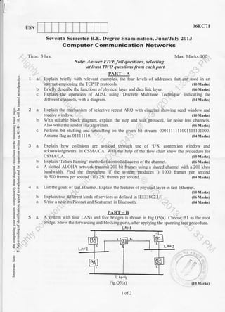
  • 1. 'l USN Time: 3 hrs. Notet Answer FIVE full questions, selecting at least TWO questions from each part. 06EC7t Max. Marks:100 of addresses that are used in an (t0 Marks) (06 Marks) (10 Marks) (06 Marks) (04 Marks) Seventh Semester B.E. Degree Examination, June/July 2013 Gomputer Gommunication Networks s .b 3c 6q) .=.l .=.9 e.. d= .> -i .i o z E PART - A I a. Explain briefly with relevant examples, the four levels 2a. b. c. 3a. 4 a. List the goals offast Ethernet. internet employing the TCP/IP protocols. (10 Marks) b. Briefly describe the functions ofphysical layer and data link layer. (06 Marks) c. Explain the operation of ADSL using 'Discrete Multitone Technique' indicating the different chaanels, with a diagram. (04 Marks) Explain the mechanism of selective repeat ARQ with diagram showing send window and receive window (10 Marks) With suitable block diagram, explain the stop and wait protocol, for noise less channels. Also write the sender site algorithm. (06 Marks) Perform bit stufling and unstuffing on the given bit stream: 0001111111001111101000. Assume 11ag as 01 1 1 1 I 10. (04 Marks) Explain how collisions are avoided through use of 'lFS, contention window and acknowledgments' in CSMA,/CA. With the help of the flow chart show the procedure for CSMA/CA. b. Explain'Token Passing' method ofcontrolled access ofthe channel. c. A slotted ALOHA network transmit 200 bit frames using a shared channel with a 200 kbps bandu,idth. Find the throughput if the system produces i) 1000 frames per second ii) 500 frames per second iii) 250 frames per second. (04 Marks) 5a. Explain the features ofphysical layer in fast Ethernet. b. Explain two different kinds of serr,,ices as defined in IEEE 802. I 1. c. Write a note on Piconet and Scatternet in Bluetooth. PART - B A sysiem with four LANs and frv"-G@ rhown in Fig.Qs(a). Choose Bl as the root bridge. Show the fbrwarding and blocking ports, after applying the spanning tree procedure. LeF,+ Fig.Qs(a) 1of2 LhNI (10 Marks)
  • 2. t , l 06EC71 b. Define repeater, bridge and router with necessary diagrams' (06 Marks) c. Differentiate between a bus backbone network and star backbone network. (04 Marks) . 6 a. An ISP is granted a block of addresses starting with 150.80.0.0/16. The ISP wants to -' distribute these blocks of2600 customers as follows: D The first group has 200 medium size business; each needs 16 addresses' ii) The second group has 400 small business; each needs 8 addresses' iii) The third grJup has 2000 households; each needs 4 addresses' ,' Design the subblocks and give the slash notation for each subblock. Find out how many adtltesses ate still available after these allocations. (10 Marks) b. eiplain briefly strategies used to handle the transition from IPv4 to IPv6. (06 Marks) c. A 'blbii;.of addressis is granted to a small organization. One of the addresses is 205.16.37.39128. What is the first address, last address and number of address in the block. 7a. Explain the 'Distarfe Vector Routing' 'for the following e1mple shown in Fig.Q7(a)' (10 Marks) (04 Marks) Briefly discuss the foltowing forwarding techniques: i) Next-Hop method versus Route method ii) Network-specific method versus Host specific method. Distinguish between diulticasting and multiple unicasting. Explain connection establishment and connection termination,in TCP. (10 Marks) write a note on DNS. (06 Marks) Write a shorri irote on source port number and destination port nurnber.in user datagram. ' (04 Marks) (06 Marks) (04 Marks) 8a. b. c. Fig.Q7(a) 2 of2
  • 3. r USN Time: 3 hrs. 068C72 Max. Marks:100 (06 Marks) (06 Marks) of glass fiber, how RI can be (04 Marks) approximately 1000 modes at an 850nm Seventh Semester B.E. Degree Examination, June/July 2013 Optical Fiber Gommunication Note: Answer FIVEfull questions, selecting at leost TWO questions from each part. o E I ai! '=^ a-a o." ,i .9 6, at= o :: 6.S o< .i ..i o z E la. b. c. PART-A Discuss the advantages and disadvantages ofOFC. Explain Mode Field Diameter (MFD) of a single mode fiber. Differentiate between glass fiber and plastic fibers. In case varied? d. A SI multimode fiber with a NA of 0.20 supports wavelength. i) What is the diameter of its core? iD How many modes does the fiber support at iii) How many modes does the fiber support at 2 a. Explain the "pulse dispersion" with suitable diagram and ditferentiate MMSIF, MMGIF and SMF by their information carrying capacity with reason. (06 Marks) b. Discuss the following for optical fibers: i) Extrinsicabsorprion. ii) Materialdispersion. c. Optical power launched into fiber at transmitter end is 150pw. The power at the end of 10km length of the link working in first window is -38.2 dBm. Another s/m of same length working in second window is 47.5 pw. Same length sim working in third window has 50% of launched power. Calculate ltber attenuation for each case and mention wavelength of operation. (06 Marks) 3 a. A double-hetero junction "lnGaAsP" LED emitting at a peak,wavelength of 1310 nm has radiative and non radiative recombination times of 25 ns and 90 ns respectively. The drive current is 35 mA. i) Find the internal quantum efficiency and the internal power. ii) If the RI of the light source material is n : J.5. Find the power emitted iiom the device. (06 Marks) b. Describe the following terms relating to LASER: i) External quantum efficiency. ii) Wavelengthspacing. c. Explain the tlree lactors which affects the response time ofa photodiode. 4 a- Discuss the different lensing scheme used to improve the source-to-fiber coupling efficiency, with the necessary sketches. (06 Marks) b. For a surface emitting LED has radiance of l50W(cm2.sr) and radius of emitting area is 35pm. Calculate the optical power coupled to the fibers with 1320 nm? 1550 nm? (04 Marks) (08 Marks) (06 Marks) (08 Marks) (06 Marks) (08 Marks) a1 = 25prm and NA : 0.20, step index a2 : 50pm and N A:0.20, step index. c. Define fiber splicing. Explain different types of splicing with neat sketches. 1 of2
  • 4. t-I 06F,C72 PART-B 5 a. Explain the different tlpes of front-end amplifiers in optical receiver. (06 Marks) b. With a neat sketch, explain how system performance information can be obtained from the eye diagram. c. Write a short note on burst-mode receivers. (08 Marks) (06 Marks) -.':g a. Following are the parameters of a point-to-point optical link: :- - i) Optical power launched : +3dBm ,. il) Sensitivity ofdetector : -32dBm r'- iii) Source/detector connector loss : 1dB 'iv), Length ofoptical cable : 60 km v1'... t'Cable attenuation : 0.3dB/kmv1'...t'Cable attenuation : 0.3dB/km vi) ' Jqrnper cable loss : 3dB vii) Co'nnector loss at each fiber :1dBLbnnector loss at eacn rlDer : lol]' r-' joint (two at each transmitter and receiver end be&trse of the jumper cables) Compute the powel margin of the link using spread sheet'mbthod' (06 Marks) b. Explain the basic eleruents of analog link with differenl nrii3e contribution. (09 Marks) c. What is sub carrier multiplexing? Explain. (05 Marks) 7 a. Explain the need of isolator iiidptical network.'Give its principle of operation also. (06 Marks) f. Explain the operational principle an! iilplementation of WDM. (08 Marks) s. Briefly discuss dielectric thin-film ftltg1C;. (06 Marks) ,'-- I '., 8 a. Explain the three main optical amplifier types. (06 Marks) b. Describe: i) SONET/SDH rings..,. ii) SONET/SDHnetworks. iii) Frame format pf STS-1 SONET. (t0 Marks) c. An EDFA amplifier'produces P..out : 27dBm for an input Pqio = 2dBm at 1542 nm. i) Find the aipplifier gai4 G. ii) Y,i: *" minimum pump power required. (04 Marks) .-. ,;..i * * * :t * 2 of2
  • 5. I USN 06EC73 (12 Marks) (02 Marks) (10 Marks) (06 Marks) E 89 te bE -a'CA tq ,i .? a,i 6.Y a3 9< - ..i o z o F Seventh Semester B.E. Degree Examination, June / July 2013 Power Electronics Time: 3 hrs. Max. Marks:100 Note: l. Answer any FIVE full questions, selecting utleost TWO question from each part. 2. Draw neat diagram and Waveforms, wherever possible. P.{RT - A I a. What is Power Electronics? Draw a neat block diagram of generalized power converter system. State the applications ofpower dlectronics. (06 Marks) b. With neat circuit diagram and waveforms. explain the rypes of power electronjc circuils. 2 a. The maximum junction temperature of a transistor is Tt : 1500C and the ambient temperature is To:250a, If the thermal impedances are &c:0.40ClW, R.,:0.1oC/W, and Rse : 0.50C/W. Calculate i) the maximum power dissipation and ii) the case c. Compare General purpose, Fast recovery and Schokky diodes. n - tlpe (enhancement) MOSFET. c. Write a note on isolation ofgate and base drives. temperature. (0,1 Marks) b. With the help of parasitic model and switching model, explain the switching waveforms of 3 a. Using a two transistor model of thyistor, show that Ie = olq + ]tuu' * Iquo' . (06 Marks) 1 - (cr, +crr) b. With neat sketch, explain turn on characteristics of SCR. (06 Marks) c. The input voltage Fig. Q3(c) is V, = 200V with load resistance of R - 5O. The load and stray inductances are negligible and the thy,ristor is operated at a frequency of f. : 2KHz. If the required dv/dt is 100 V/pS and the discharge current is limited to 100,4.. Determine i) the values ofR. and C. ii) the snubber loss, and iii) the power rating of the snubber resistor. (08 Marks) Pi3 . q3 c.d"/dv Y*u.-..t.,,,., C.,r.cliL 4a. b. c. Discuss the effect of inductance using the 1 - O full converter. (08 Marks) What is phase control? Explain the principal of phase control using 1 - $ half wave controlled rectifier. (08 Marks) Compare circulating and non - circulating mode ofoperation ofdual converter. (04 Marks) 1 of 2
  • 6. I b. 06EC73 PART-B A thyistor circuit is shown in fig. Q5(a), if thyristor Tr is switched on at t: 0, determine the conduction time of thyristor Tr and the capacitor voltage after Tr is tumed off. The circuit parameters are L : l0pH, C - 50pF and V' - 200V. The inductor carries an iniiial current oflm = 250A. (10 Marks) e Pl5 , 4.5a : o"t5 c..,r-*t^ u.J a.r. c- i t_ is ihe principle of complementary commutation? Explain the same with the help of suitable circuit and waveforms. (10 Marks) What is the principle of on off control? Explain the sanie r,nith a single phase full - wave controller. (06 Marks) Draw a neat sketch of 1 - $ AC voltage controller with RL load and explain its working. (06 Marks) c. A single - phase full wave AC voltage controller has a resistive load of R: l0 O and the input voltage is V.: 120V (rms), 60H2. The delay angles of thyristors Tr and T2 ilre eQual ol : 02: r/2. Determine i) the rms output voltage V" ii) the input power factor PF iii) the average current ofth},ristor Inand iv) the rms current ofthlaistor IR. (08 Marks) With a neat circuit diagram, explain the operation of a step down chopper and also explain constant frequency and variable frequency operation. Derive an expression for output voltage incase ofstep down chopper. (10 Marks) b. A step - up chopper with a pulse width of200ps operating on 200V, dc supply. Calcualte the output voltage, ifthe blocking period ofthe device is 50ps. (02 Marks) c- With a neat and quadrant operation, explain class E chopper. (08 Marks) a. With a neat circuit diagram, of 1 - { half bridge inverter, explain the principle of operation ofan inverter. (08 Marks) b. write briefnote on current source inverter. , (06 Marks) c. With the help of circuit diagram and waveforms, explain a variable DC -,trO t"u.[?.nnurur, 2 of2
  • 7. USN 068C74 TMS320C54XX (10 Marks) either on-chip or (06 Marks) located in (04 Marks) Seventh Semester B.E. Degree Examination, June/Juty 2013 c. d. g I te :q 56 9JE G- tq r--) < -i ..i a z A E DSP Algorithms and Architecture Time: 3 hrs. Max. Marks:100 Note: Answer FIVE fult questions, selecting at least TWO questions from each part. PART_A I a' List and explain the issues that have to considered in designing and implementing a DSp system. (04 Marks) [. lmplement an FIR firter ror y(n)- (xtn)+x(n -l)+xtn-2)). Determine the (i) sysrem function (ii) magnitude response function (iii) phase response function. Plot its magnitude and phase response. (06 Marks) c. Explain the process of decimation. (04 Marks) d The signal sequence x(n) : [0 2 4 6 Sl is interpolated using the interpolation filter sequence h : [0.5 1 0.5] and the interpolation factor is 2. Deiermine thi interpolated sequence y(m). (06 Marks) b. Explain the different frequently used teohniqries to prevent overflow and underflow conditions occuning in MAC unit. (04 Marks) Explain the diftbrent ways in which the on-chip memory can be organized efficiently and cost-effective manner. (04 Marks) Explain the register pointer updating algorithm for circular buffer addressing mode. (04 Marks) I-.ist the techniques used in DSP architecture to increase speed of operation and operations that should be accomplished in single clock to achieve purull.li.- in DSp iomplementation. (08 Marks) Explain with a neat clock diagram the indirect addressing mode of processor. Give the operand syntax and operation for the followins: i) Circular addressing mode ii) Bit reverse addressing mode. Ex-plain the different ways in which PC addresses the program memory off-chip and gets loaded for execution ofinstructions. Specifl the on-chip memory configurarion lor Mpl MC, OVLy and DROM processor mode status register of 5416 processor. Describe the operation and application of the following instructions of rMS320c54XX processor with example: i,) MAC i, MAS iii) LD *AR4,4, A Given contents ofAR4 is 8boeh& SxM: l. Determine the contents ofaccumulator. (06 ,larks) Write an ALP of TMS320C54XX processor to compute {n) = h cos x(n) + h(1) x(n - l) + h(2) x(n - 2), using MAC instruction, where h(0) : 5, h(l) : 31, h(2) : 13 are in program memory loiations starting at tr. 4n) '= t, x(n- 1):5 x(n - 2)= -3 are in data memory locations starting at iy(n) is to be saved (lo.wer 16 bits) in location y and y +l (higher 16 bits). (0s Marks) With a neat sketch, describe the Host port interface signals. 1Or tr.lart<g Explain the six-stage pipelined execution of TMS320C54XX. .i , , ios tuartg I of 2 3a. b. c. 4a. b. c. d.
  • 8. a program for a second order IIR filter on TMS320C54XX processor defined by the transfer function H(z) - 0.104 - 0.1022-1 + 0.1042-2 Assume that the filter 1+ z-t - 0.6122-2 poefficients are qls numbers x(n) is the input sample (integer), input samples. are placed in i tnrffer, insamples, fiom a data file, data-in.dat. y(n) is computed output. The output samples ard placed in a buffer outsamples. (10 Marks) c. Explain-with necessary block diagram, memory organization for implementing FIR filter of orderN.-'.. (05 Marks) 6 a. Determine the following for a 512 point FFT computation : i) Number of stages ii) Number of butterflies in each stage iii) Number of butterflies needed [or the entire computation. iv) Number ol butterllies that need no twiddle lactors. v) Number of butterflies ttial require real twiddle factors vi) Number of butterflies that require complex twiddle factors. (06 Marks) b. Explain how scaling prevents overflow conditions in the butterfly computation. (06 Marks) c. Write a TMS320C54XX program'segment that implements 8 point DIT FFT bit reversed PART _ B Explain Q7 and Qrs Notations with example. 068C74 (05 Marks) (08 Marks) DSP in the address range (06 Marks) IIO ND (06 Marks) (08 Marks) (06 Marks) (O8 Marks) 5 a. Define Q Notation. b. Realize and write index generation and to clear FFT dlrta memory. '...'' 7 a. Interface an 8kx 16 prqsaril ROM to the C5416 TFEOOOh _ TFFFFFh. b. Explain with a flow''chdrt diagram for software polling for the programmed converter interface. c. Define intemrpt. Write a flow chart of interrupt handling by C54XX processor. 8 a. Explafuriith neat block diagram the PCM 3002 interfaced to TMS320VC5416 in the DSK. (06 Marks) b. .Explain with block diagram the biotelemetry receiver implementation. i.. 'With a neat sketch, explain the JPEG encoder and decoder. ***** 2 of2
  • 9. / USN PART - B WIy smoothing is needed in image processing? What is ideal LPF and Butterworlh LPF in the above context. accomplish this. 06EC756 its effect on the image? ExPlain an (10 Marks) to transform the in Fig.Qs(b)(ii). and z that will (10 Marks) I o o g@ ;g o'o i: _: -9= 9< Z o E Seventh Semester B.E. Degree Examination, June/July 2013 lmage Processing Time: 3 hrs. Max. Marks:100 Note': Answer FIVEfull questions, selecting at least TWO questions from each parl PART - A I a. with a neat block diagram explain the fundamental steps in digital processing. (10 Marks) b. Consider the two image subsiates Sr and Sz shown in Fig.Ql(b). For V: < 1 >, determine whether these two subsets are: i) 4-adiacent, ii) S-adjacent or (iii) M-adjacent. (10 Marks) S1 S2 D I I o O l ll Ao ll l Fig.Ql(b) 2 a. Explain the role of sampling and Quantization in image processing system' (10 Marks) b. what are the basic relationships between pixels? with neat diagrams and appropriate mathematical expressions, explain (i) neighbours, ii) adjacency, iii) connectivity. (t0 Marks) 3 a. With respect to 2D discrete Fourier transform of an image, explain the following, derive suitable equations: i) Separability ii) Transition iii) Rotalion iv) Periodicity (10 Marks) b. Explain the homomorphic filtering approach fbr image enhancement (10 Marks) 4 a. Give the expression for Hadamord transform and generate the corresponding 1-D Kernal for N :4. Explain any two ofits properties. (12 Marks) b. Write an explanatory note on Histogram equalization. (08 Marks) 5a. b. An image has the gray level pdf p(r) shown in Fig.Q5(b)(i). It is desired gray levels of this images so that they will have the specified p(z) shown Assume continuous quantities and find the transformation in terms of r ? Lz) ootl oloo rtDo o ao o o o oo oo oolo otll Pie.Qs(b)(i) 1of2
  • 10. 6 a. With the help of a neat graphical illustration, explain the powerJaw piecewise linear contrast stretch. b. Explain how image degradation is carried out using: 06EC7s6 transformation and (10 Marks) (10 Marks) (10 Marks) (10 Marks) , r'.' .'.':.] -. r 1"..1i_ .-..i. t 2 of2
  • 11. T]SN Seventh Semester B.E. Degree Examination, June/July 2013 -s --t dql] 0r i; i. (E do 6'= o- ;i ca -i c.i o z E 1a. b. 4 a. Explain scope and visibility of a variable. b. What are the basic language requirements for RT language? Explain. c. What is CUTLASS? What are the requfuements of CUTLASS? PART - B 5 a. Explain dilTerent scheduling strategies. b. Three cyclic tasks A, B, C are required to run at 1 tick, 2 ticks and (1 tick : 20 ms). Assuming tasks A, B, C consumes 5 ms, 8 ms and Write task activation diagram lor priority order. (Context switching time i) A (highest), B, C ii) B (highest), A, C c. What is code sharing? Explain serially reusable and re-entrant code. Real Time Systems Time: 3 hrs. Notez Answer FIVE full questions, selecting dt least TWO questions from each part' PART-A Give two definitions for real time system. Explain dilferent classifications ol RTS based on synclronization 6 a. With a neat diagram, explain the general structure of IOSS. b. Explain the problem of shared memory. How semaphores are problem? c. Explain Liveness. a. Explain foreground and background system with a flowchart. b. Differentiate pool and channel. c. Explain software design for RTS using software module. a. Explain lunctional specifications with respect to a drying oven. b. Explain Yourdon methodologY. c. With a relevant diagram, explain Ward and Mellor's method' and intemal tasks ofthe comPuter. c. Explain hard and soft RTS with relevant equations. 2 a. Compare batch processing and continuous processing b. With a neat diagram, explain distributed systems with its advantages. c. Write a note on supervisory control systems. 3 a. The clock on computer generates an interrupt for every 20 ms' Draw a flow chart for interrupt service routine, *hi.h hu, to keep a 24 hour clock in terms of hours, minutes and seconds' (08 Marks) b. Explain a simple digital input and output interiaces. (10 Marks) c. Write a note on different LAN topologies. (02 Marks) o6EC762 Max. Marks:100 (04 Marks) between external process (08 Marks) (08 Marks) (05 Marks) (10 Marks) (05 Marks) (04 Marks) (10 Marks) (06 Marks) (06 Marks) 3 ticks respectively 10 ms respectively. : 0). (06 Marks) (08 Marks) (07 Marks) used to overcome this (09 Marks) (04 Marks) (10 Marks) (04 Marks) (06 Marks) (07 Marks) (05 Marks) (08 Marks).