project report on embedded system
•Transferir como DOCX, PDF•
8 gostaram•2,682 visualizações

Summer training project report on embedded system at BSNL ALTTC Ghaziabad. Submitted by RAM AVTAR (ECE Department of IMSEC) of 2016 Batch. Submitted in IMS Engineering College, Gaziabad

Recomendados
Recomendados
Mais conteúdo relacionado
Mais procurados
Mais procurados (20)
Destaque
Destaque (13)
Semelhante a project report on embedded system
Semelhante a project report on embedded system (20)
Último
Último (20)
project report on embedded system
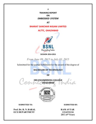
- 1. A TRAINING REPORT ON EMBEDDED SYSTEM AT BHARAT SANCHAR NIGAM LIMITED ALTTC, GHAZIABAD SESSION 2014-2015 From June 09, 2015 to July 03, 2015 Submitted for the partial fulfillment for the award of the degree of BACHELOR OF TECHNOLOGY OF IMS ENGINEERING COLLEGE GHAZIABAD SUBMITTED TO: SUBMITTED BY: Prof. Dr. R. N. BARAL RAM AVTAR ECE DEPARTMENT 1214331124 2EC (4th Year)
- 2. DECLARATION I RAM AVTAR, student of IMSEC GHAZIABAD of B.Tech 4th year(7th semester) hereby declare thatI havecompletedthis Summer Training in BSNL ALTTC, GHAZIABAD in Academic year2014-2015.My Certificate Number is ALTITNB300-2015- 1456013 . The information submitted is true and original to the best of my knowledge. RAM AVTAR (1214331124) 2EC 4th Year
- 3. Acknowledgment I am truly thankful to all the faculties who imparted the lectures on various subjects/topics and took us to the plant in a guided study visit along with detailed explaining about the plant and machinery. An Electronics student mainly focuses on practical applications of concepts learned projects like this one provide us with an ideal opportunity to do the same .I acknowledge the valuable inputs provided by Mr. NEERA GUPTA . Last but not least, a big thanks to all my family members and friends, for timely cooperation and support extended to me all the way. RAM AVTAR 1214331124 2EC 4th Year
- 4. INDEX S. No. Contents Page No. 1. Overview of Embedded Systems 2 2. Introduction to Atmega16 microcontroller 3 3. Analog to Digital converter 5 4. Timers in Atmega16 7 5. 7 segment Interfacing 8 6. LCD Interfacing 9 7. IR Sensor Interfacing 10 8. LM35 Interfacing 11 9. Matrix keypad interfacing 12 10. DTMF interfacing 13 11. RGB LED interfacing 15 12. Relay interfacing 16 13. Touchscreen interfacing 17 14. Major and Minor projects done 19 15. Preferences 19 16. Certificate of Summer Training 20
- 5. 1. Embedded Systems Introduction:- Embedded system is a scaled down computer system which is designed to perform a specifictask or operation. The whole system is embeddedinto an appliance.This reduces human effortto a greatextent. A single chip contains both hardware and software. Some importantthings to note aboutembedded systems: 1. Once an embedded hardware is programmed fora certain task, it is used foreverfor the same task. Changing the firmware afterwards is not possible. 2. Such systems are limited in computational resources like memory, CPU processing speed, I/O facilities but are still capable of performing the task given to them very efficiently. 3. Embeddedsystems canalso be having a reduced functionality version of operating system called RTOS (Real Time Operating System) for highly specialized applications. 4. Interacts with physical elements in our environment, viz. controlling and driving a motor, sensing temperature, etc. EMBEDDED SYSTEM IN DAILY LIFE Digital Clock Traffic Light DVD Player Smart Phones 2. MICROCONTROLLER A Microcontroller is a programmabledigital processor with necessary peripherals. Both microcontrollers and microprocessorsare complex sequential digital circuits meant to carry out job according to the program / instructions. ATMEGA16 MICROCONTROLLER: We will be working on Atmega16 microcontroller,which is a 40-pin IC and belongs to the MegaAVR category of AVR family.
- 6. Some of the features of Atmega16 are: 16KB of Flash memory 1KB of SRAM 512 Bytes of EEPROM Available in 40-Pin DIP 8- Channel 10-bit ADC Two 8-bit Timers/Counters One 16-bit Timer/Counter 4 PWM Channels Serial USART Digital to Analog Comparator PIN DIAGRAM I/O PORTS Input Output functions are set by Three Registers for each PORT. • DDRX ‐‐‐‐> Sets whether a pin is Input or Output of PORTX. • PORTX ‐‐‐> Sets the Output Value of PORTX. • PINX ‐‐‐‐‐> Reads the Value of PORTX. (Where X= A, B, C or D) DDRX (Data DirectionRegister) Now to make a pin act as I/O we set its corresponding bit in its DDR register. • To make Input set bit 0 • To make Output set bit 1 PORTX(PORTXData Register) If a pin is set to be output, then by setting bit 1 we make output High that is +5V and by setting bit 0, make output Low that is 0V. If a pin is set to be input, then by setting its corresponding bit in PORTX register will make it as follows, Set bit 0 ‐‐‐> Tri‐Stated Set bit 1 ‐‐‐> Pull Up. PORTX ‐‐‐‐> to set value of PORTX with a byte. PORTX.y ‐‐> to set value of yth pin of PORTX with a bit (works only with CVAVR).
- 7. PINX (Data Read Register) This register is used to read the value of a PORT. If a pin is set as input then corresponding bit on PIN register is, • 0 for Low Input that is V < 2.5V • 1 for High Input that is V > 2.5V (Ideally, but actually 0.8 V ‐ 2.8 V is error zone!) • PINX ‐‐‐‐> Read complete value of PORTX as a byte. • PINX.y ‐‐> Read yth pin of PORTX as a bit (works only with CVAVR). SOFTWARE The software which support this hardware and can communicate with micro controller using this circuit is- • AVRStudio 4 3. Analog to Digital Converters Microcontroller understands only digital language. To convert the analog output from the sensors to digital we need ADC. In AVR family of microcontroller we have inbuilt ADC on PORTA. Each pin in PORTA has an ADC circuit connected behind it. Thus we have 8 channels of ADC. The resolution of ADC output is 10 bit i.e. the output from the ADC is any number between 0 to 1023 ADC registers: The inbuilt ADC of AVR microcontroller have three register which are used for configuring the ADC. They are: ADMUX: it is used for selecting the ADC pin to be used for connecting the Analog sensors.Itis also used forsetting the reference value of the ADC. ADSCRA:itis used forcontrolling the ADC e.g.when should it start the conversion? Should it repeat the conversion? Should interrupt be generated after the conversion is complete? Etc. ADCH & ADCL: these are used for storing the ADC output values. Both the registers are 8 bit wide and we require 10 bits for storing the ADC value. Thus the two registers are used. The way of storing the ADC value is configured using ADSCRA. ADMUX
- 8. ADLAR:-This bit is setting the manner, the ADC result will be stored in ADC data register. ADLAR = 0 ADCH& ADCL ADCSR 4. Timers in ATMega16 In Atmega16, we have three timers:TIMER0 TIMER1 and TIMER2 Out of these, TIMER0 and TIMER2 are 8 bit timer, while TIMER1 is a 16 bit timer. All the timers have three unique registers and two common registers. TIMER1 has a special register, called ICR(Input Capture Register).It has two channels(channel A and channel B). TIMER2 has a specialregister known as ASSR, which is used two generate PWM using asynchronous clock.
- 9. Timer Registers • Each timer has three registers. They are: TCCR(Timer Counter Control Register) TCNT(Timer Counter), OCR (Output Compare Register). • Thus, three registers for TIMER0 are TCCR0, TCNT0 and OCR0. • Similarly for TIMER1 and TIMER2, we have TCCR1, TCNT1, OCR1 and TCCR2, TCNT2 and OCR2. • The three timers have two common registers. They are: TIMSK (Timer Interrupt Mask) TIFR (Timer Interrupt Flag Register Register Function Description • TCCR (Timer Counter Control Register): It is used for configuring the timer i.e. modes and pre scale factor. • TCNT: It stores the present value of the timer. It is used for monitoring the status of the timer. After each incrementing in the timer value, this register compares its value with the OCR register value. • OCR(Output Compare Register): It is used for setting the required duty Cycle 5. Seven Segment Display Interfacing • A seven-segmentdisplaycan be used to display the decimal numbers 0-9 and some alpha characters. • A Seven-Segment Display (SSD) is simply a figure eight grouping of LEDs {include a decimal point (DP)}. • Each Segment is labeled (a) to (g). • SSDs are available in two configurations • Common Cathode (all LED cathodes are connected) • Common Anode (all LED anodes are connected)
- 10. Fig: Interfacing with atmega16 fig: 7Segment display 6. LCD INTERFACING • LCD’s are all around us so liquid crystal displays are very useful in these days. • It is a kind of display that is made up of a special matter state formed using liquid and crystal both , it’s a forth state of matter • The most popular one is 16x2 LCD module.It has 2 rows & 16 columns. The intelligent displays are two types: Text Display Graphics Display PIN DESCRIPTION Figure 4.1: pin configuration for 16 X 2 LCD 8 data pins D7:D0 Bi-directional data/command pins. Alphanumeric characters are sent in ASCII format. RS: Register Select RS = 0 -> Command Register is selected RS = 1 -> Data Register is selected R/W: Read or Write 0 -> Write, 1 -> Read E: Enable (Latch data) Used to latch the data present on the data pins. A high-to-low edge is needed to latch the data. VEE: contrast control.
- 11. VDD & VSS: Power supply VDD= +5V VSS=GND 7. IR Sensor interfacing There are two part of the sensors: 1. Emitter 2. Receiver Emitter converts the electrical current in the Infra-Red Radiation. Receiver receive the IR radiation when the radiation reflect back after the collision from the obstacle and then this IR radiation is converted into electrical current. OperatingModes: Our IR sensor can work in two modes: Analog Mode: - In this the output is continuously changes depending upon the reflections from the objects. Digital Mode:- In this the output is constant either high or low depending upon reflections. How to use? • Digital Mode:-In this mode you can directly connect the sensor to any pin of the controllerand can perform any task according to the condition you mentioned in program. • Analog Mode:-Inthis mode sensorwillgive analog value so you have to use ADC because microcontroller works on digital 8. LM35 INTERFACING • LM35 is a precision IC temperature sensorwith its output proportional to the temperature (in o C). The sensor circuitry is sealed and therefore it is not subjected to oxidation and other processes. With LM35, temperature can be measured more accurately than with a thermistor. It also possess low self- heating and does not cause more than 0.1 o C temperature rise in still air.
- 12. • The operating temperature range is from -55°C to 150°C. The output voltage varies by 10mV in responseto every o C rise/fall in ambient temperature, i.e., its scale factor is 0.01V/ o C. Pin Diagram Output • Output of the temperature sensor is analog so we cannot measure it directly from the controller because it works on a digital logic so we have to initialize ADC of the controller. • Give the output of analog sensor on PORTA 9. Interfacing matrix keypad • The matrices are actually an interface technique. It can be used to interface inputs like the PC keyboard keys, but also to control multiple outputs like LEDs.According to this technique, the I/O are divided into two sections: the columns and the rows. • It is basically a two dimensional array. We are connected switched in a fashion as shown in figure. This is 4x4 keypad matrix which is having two four pin connector. One connector is connected with PORTC and another is from PORTA. As there are only four pins so we can connect these pins from lower or higher pins of the MCU PORTs. Flow chart of using this KEYPAD- Connect connectors from PORTs. Make one PORT as input and another as output (configuration of DDR). Give ground to one connector’s pin using output configured PORT and read the corresponding pin of input configured PORT. Pin No Function Name 1 Supply voltage; 5V (+35V to -2V) Vcc 2 Output voltage (+6V to - 1V) Output 3 Ground (0V) Ground
- 13. 10. DTMF Interfacing • The invention of this is attributed to WesternElectric and first used by the Bell System in commerce. • DTMF signals are the superposition of 2 sine waves with different frequencies. • It is a signaling Technology used for communicating between two far away devices. • It uses frequency of speech signals. • Only 12 tones are used by our mobile communication out of the 16 combination that are possible. • The DTMF is a popular signaling method between telephones and switching centers. DTMF Tone Generation • EXAMPLE:-Pressing the key 1 will result in a sound composed of both a 697 and a 1209 hertz (Hz) tone. Decoding DTMF
- 14. • The CM-8870 is a full DTMF Receiver that integrates both band split filter and decoderfunctions into a single18-pinDIP or SOIC package. If I am pressing a key let say 1, then it will give the combination of Frequencies 1209 & 697, and this will directly be given to our sound Converter IC, the output of that IC would be 0001(Q1, Q2, Q3, Q4), Following table shows the output for remaining keys. 11. RGB LED interfacing • It’s is similar to a normal LED but the difference is that it can emit every possible color.As its name suggestthat it has three LED’s inside it of Red, Green and Blue color. • It has Four LEGS, in which one is common and remaining three are for R, G and B color. 12. RELAY INTERFACING • A relay is a simple electromechanical switch made up of an electromagnet and a set of contacts. • Relays are used where it is necessary to control a circuit by a low- power signal (with complete electrical isolation between control and controlled circuits), or where several circuits must be controlled by one signal
- 15. • Provide a sufficient amount of current to this relay, an extra circuit is also require because microcontroller is not capable of providing such current, that’s why ULN2803 IC is used for this purpose. 13. Touch screen interfacing • A TouchScreen is an electronic visual display that the user can control through simple ormulti-touch gestures bytouching the screenwith one or more fingers.Some Touch Screen can also detect objects such as a stylus or ordinary or specially coated gloves Types of Touch Screen: • Resistive Touch Screen • Capacitive Touch Screen • Infrared Touch Screen • Surface Acoustic Wave • Optical Imaging Resistive Touch Screen • Resistive touchscreenis a relatively new technologywhich utilizes two flexible sheets that are separated by air gaps and coated by resistive material • Pressure applied to the surface of the display by a finger or stylus causes the layers to touch, which completes electricalcircuits and tells the device where the user is touching. Detecting a Touch To know if the coordinate readings are valid, there must be a way to detect whether the screen is being touched or not. This can be done by applying a positive voltage (VCC) to Y+ through a pull up resistor and applying ground to X–.
- 16. When there is no touch, Y+ is pulled up to the positive voltage. When there is a touch, Y+ is pulled down to ground as shown in Figure1. This voltage-level change can be used to generate a pin-change interrupt. How it works A uniform voltage gradient is applied to one sheet.whenever the second sheet touches the other sheet, the second sheet measures the voltage as a distance along the first sheet. This combinaton of voltage and distance provides X cordinate. after the X cordinate is located, entire process repeats itself by applying uniform voltage gradient to the second sheet inorder to find the Y cordinate.this entire process happens in a matter of milliseconds,oblivious to human eye. As it’s also a kind of sensing device so, will give the output in analog form. Again we need to convert this form into digital form. That’s why we need a ADC.
- 17. 14. Projects done during training Minor Projects Project 3: Wall Follower Robot Project 8: High Temperature Alarm 15. Preferences Prof. Neeraj Gupta www.google.com www.bsnl.co.in www.wikipidea.com