Microcontroller 8051 gs
•Transferir como PPT, PDF•
3 gostaram•1,596 visualizações

The document discusses the Intel 8051 microcontroller family. It provides a brief history of the 8051, noting it was introduced in 1980 and had 128 bytes of internal RAM and 4Kbytes of ROM. It then lists several manufacturers of 8051 variants and their key features. The rest of the document goes into more detail about the hardware architecture of the 8051, including the pin descriptions and functions of the ports, timers, and serial interface.

Recomendados
Mais conteúdo relacionado
Mais procurados
Mais procurados (20)
Semelhante a Microcontroller 8051 gs
Semelhante a Microcontroller 8051 gs (20)
Último
Último (20)
Microcontroller 8051 gs
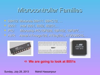
- 1. Sunday, July 28, 2013 Mahdi Hassanpour Microcontroller FamiliesMicrocontroller Families 68H12: Motorola 68H11, 68HC12, …68H12: Motorola 68H11, 68HC12, … 8051: Intel 8051, 8052, 80251,…8051: Intel 8051, 8052, 80251,… PIC: Microchip PIC16F628, 18F452, 16F877, …PIC: Microchip PIC16F628, 18F452, 16F877, … AVR: Atmel ATmega128, ATtiny28L, AT90S8515,…AVR: Atmel ATmega128, ATtiny28L, AT90S8515,… We are going to look at 8051s
- 3. Sunday, July 28, 2013 Mahdi Hassanpour 8051 History8051 History Introduced 1980Introduced 1980 12 MHz12 MHz 128128 bytesbytes Internal RAMInternal RAM 4 Kbytes ROM4 Kbytes ROM 1 Serial port support1 Serial port support
- 4. Sunday, July 28, 2013 Mahdi Hassanpour 8051 Manufacturers8051 Manufacturers AMD: Enhanced 8051AMD: Enhanced 8051 partsparts (no longer producing 80x51 parts)(no longer producing 80x51 parts) Atmel: FLASH and semi-custom partsAtmel: FLASH and semi-custom parts Dallas: Battery backed, program download, and fastestDallas: Battery backed, program download, and fastest variantsvariants Intel: 8051 through 80c51gb / 80c51slIntel: 8051 through 80c51gb / 80c51sl ISSI: IS80C51/31 runs up to 40MHzISSI: IS80C51/31 runs up to 40MHz Matra: 80c154, low voltage static variantsMatra: 80c154, low voltage static variants OKI: 80c154, mask partsOKI: 80c154, mask parts Philips87c748 thru 89c588 - more variants than anyone elsePhilips87c748 thru 89c588 - more variants than anyone else – now NXPnow NXP Siemens: 80c501 through 80c517a, and SIECO coresSiemens: 80c501 through 80c517a, and SIECO cores SMC: COM20051 with ARCNET token bus network engineSMC: COM20051 with ARCNET token bus network engine SSI: 80x52, 2 x HDLC variant for MODEM useSSI: 80x52, 2 x HDLC variant for MODEM use
- 5. Why do we need to learnWhy do we need to learn Microprocessors/controllers?Microprocessors/controllers? The microprocessor is the core of computer systems. Nowadays many communication, digital entertainment, portable devices, are controlled by them. A designer should know what types of components he needs, ways to reduce production costs and product reliable..
- 6. Different aspects of a microprocessor/controller Hardware :Interface to the real world Software :order how to deal with inputs
- 7. The necessary tools for aThe necessary tools for a microprocessor/controllermicroprocessor/controller CPU: Central Processing Unit I/O: Input /Output Bus: Address bus & Data bus Memory: RAM & ROM Timer Interrupt Serial Port Parallel Port
- 8. CPU General- Purpose Micro- processor RAM ROM I/O Port Timer Serial COM Port Data Bus Address Bus General-Purpose Microprocessor System Microprocessors:Microprocessors: CPU for Computers No RAM, ROM, I/O on CPU chip itself Example : Intel’s x86, Motorola’s 680x0 Many chips on mother’s board General-purpose microprocessor
- 9. RAM ROM I/O Port Timer Serial COM Port Microcontroller CPU A smaller computer On-chip RAM, ROM, I/O ports... Example : Motorola’s 6811, Intel’s 8051, Zilog’s Z8 and PIC 16X A single chip Microcontroller :
- 10. Microprocessor CPU is stand-alone, RAM, ROM, I/O, timer are separate designer can decide on the amount of ROM, RAM and I/O ports. expansive versatility general-purpose Microcontroller • CPU, RAM, ROM, I/O and timer are all on a single chip • fix amount of on-chip ROM, RAM, I/O ports • for applications in which cost, power and space are critical • single-purpose Microprocessor vs. Microcontroller
- 11. Embedded system means the processor is embedded into that application. An embedded product uses a microprocessor or microcontroller to do one task only. In an embedded system, there is only one application software that is typically burned into ROM. Example : printer, keyboard, video game player Embedded System
- 12. 1. meeting the computing needs of the task efficiently and cost effectively • speed, the amount of ROM and RAM, the number of I/O ports and timers, size, packaging, power consumption • easy to upgrade • cost per unit 2. availability of software development tools • assemblers, debuggers, C compilers, emulator, simulator, technical support 3. wide availability and reliable sources of the microcontrollers. Three criteria in Choosing a Microcontroller
- 13. Block DiagramBlock Diagram CPU On-chip RAM On-chip ROM for program code 4 I/O Ports Timer 0 Serial PortOSC Interrupt Control External interrupts Timer 1 Timer/Counter Bus Control TxD RxDP0 P1 P2 P3 Address/Data Counter Inputs
- 15. Sunday, July 28, 2013 Mahdi Hassanpour PackagingPackaging Plastic Dual In-Line package (PDIL)Plastic Dual In-Line package (PDIL)
- 16. Sunday, July 28, 2013 Mahdi Hassanpour Packaging IPackaging I Very small Quad Flat Package (VQFP)Very small Quad Flat Package (VQFP)
- 17. Sunday, July 28, 2013 Mahdi Hassanpour Packaging IIPackaging II Plastic Leaded Chip Carrier (PLCC)Plastic Leaded Chip Carrier (PLCC)
- 18. Pin Description of the 8051Pin Description of the 8051 1 2 3 4 5 6 7 8 9 10 11 12 13 14 15 16 17 18 19 20 40 39 38 37 36 35 34 33 32 31 30 29 28 27 26 25 24 23 22 21 P1.0 P1.1 P1.2 P1.3 P1.4 P1.5 P1.6 P1.7 RST (RXD)P3.0 (TXD)P3.1 (T0)P3.4 (T1)P3.5 XTAL2 XTAL1 GND (INT0)P3.2 (INT1)P3.3 (RD)P3.7 (WR)P3.6 Vcc P0.0(AD0 )P0.1(AD1) P0.2(AD2 )P0.3(AD3) P0.4(AD4) P0.5(AD5) P0.6(AD6) P0.7(AD7) EA/VPP ALE/PROG PSEN P2.7(A15) P2.6(A14 )P2.5(A13 )P2.4(A12 )P2.3(A11 )P2.2(A10) P2.1(A9) P2.0(A8) 8051 (8031)
- 19. Pins of 8051Pins of 8051 Vcc ( pin 40 ): – Vcc provides supply voltage to the chip. – The voltage source is +5V. GND ( pin 20 ): ground XTAL1 and XTAL2 ( pins 19,18 )
- 20. Figure (a). XTAL Connection to 8051Figure (a). XTAL Connection to 8051 C2 30pF C1 30pF XTAL2 XTAL1 GND Using a quartz crystal oscillator We can observe the frequency on the XTAL2 pin.
- 21. Pins of 8051Pins of 8051 (( 2/42/4 )) RST ( pin 9 ): reset – It is an input pin and is active high ( normally low ) . The high pulse must be high at least 2 machine cycles. – It is a power-on reset. Upon applying a high pulse to RST, the microcontroller will reset and all values in registers will be lost. Reset values of some 8051 registers
- 22. Figure (b). Power-On RESET CircuitFigure (b). Power-On RESET Circuit 30 pF 30 pF 8.2 K 10 uF + Vcc 11.0592 MHz EA/VPP X1 X2 RST 31 19 18 9
- 23. Pins of 8051Pins of 8051 (( 3/43/4 )) /EA ( pin 31 ): external access – There is no on-chip ROM in 8031 and 8032 . – The /EA pin is connected to GND to indicate the code is stored externally. – /PSEN & ALE are used for external ROM. – For 8051, /EA pin is connected to Vcc. – “/” means active low. /PSEN ( pin 29 ): program store enable – This is an output pin and is connected to the OE pin of the ROM.
- 24. Pins of 8051Pins of 8051 (( 4/44/4 )) ALE ( pin 30 ): address latch enable – It is an output pin and is active high. – 8051 port 0 provides both address and data. – The ALE pin is used for de-multiplexing the address and data by connecting to the G pin of the 74LS373 latch. I/O port pins – The four ports P0, P1, P2, and P3. – Each port uses 8 pins. – All I/O pins are bi-directional..
- 25. Pins of I/O PortPins of I/O Port The 8051 has four I/O ports – Port 0 ( pins 32-39 ): P0 ( P0.0 ~ P0.7 ) – Port 1 ( pins 1-8 ) : P1 ( P1.0 ~ P1.7 ) – Port 2 ( pins 21-28 ): P2 ( P2.0 ~ P2.7 ) – Port 3 ( pins 10-17 ): P3 ( P3.0 ~ P3.7 ) – Each port has 8 pins. Named P0.X ( X=0,1,...,7 ) , P1.X, P2.X, P3.X Ex : P0.0 is the bit 0 ( LSB ) of P0 Ex : P0.7 is the bit 7 ( MSB ) of P0 These 8 bits form a byte. Each port can be used as input or output (bi-direction).
- 26. Hardware Structure of I/O PinHardware Structure of I/O Pin Each pin of I/O ports – Internal CPU bus : communicate with CPU – A D latch store the value of this pin D latch is controlled by “Write to latch” – Write to latch = 1 : write data into the D latch – 2 Tri-state buffer : TB1: controlled by “Read pin” – Read pin = 1 : really read the data present at the pin TB2: controlled by “Read latch” – Read latch = 1 : read value from internal latch – A transistor M1 gate Gate=0: open Gate=1: close
- 27. D LatchD Latch::
- 28. A Pin of Port 1A Pin of Port 1 8051 IC D Q Clk Q Vcc Load(L1) Read latch Read pin Write to latch Internal CPU bus M1 P1.X pinP1.X TB1 TB2 P0.x
- 29. Writing “1” to Output Pin P1.XWriting “1” to Output Pin P1.X D Q Clk Q Vcc Load(L1) Read latch Read pin Write to latch Internal CPU bus M1 P1.X pinP1.X 8051 IC 2. output pin is Vcc1. write a 1 to the pin 1 0 output 1 TB1 TB2
- 30. Writing “0” to Output Pin P1.XWriting “0” to Output Pin P1.X D Q Clk Q Vcc Load(L1) Read latch Read pin Write to latch Internal CPU bus M1 P1.X pinP1.X 8051 IC 2. output pin is ground1. write a 0 to the pin 0 1 output 0 TB1 TB2
- 31. Reading “High” at Input PinReading “High” at Input Pin D Q Clk Q Vcc Load(L1) Read latch Read pin Write to latch Internal CPU bus M1 P1.X pin P1.X 8051 IC 2. MOV A,P1 external pin=High 1. write a 1 to the pin MOV P1,#0FFH 1 0 3. Read pin=1 Read latch=0 Write to latch=1 1 TB1 TB2
- 32. Reading “Low” at Input PinReading “Low” at Input Pin D Q Clk Q Vcc Load(L1) Read latch Read pin Write to latch Internal CPU bus M1 P1.X pin P1.X 8051 IC 2. MOV A,P1 external pin=Low1. write a 1 to the pin MOV P1,#0FFH 1 0 3. Read pin=1 Read latch=0 Write to latch=1 0 TB1 TB2
- 33. Other PinsOther Pins P1, P2, and P3 have internal pull-up resisters. – P1, P2, and P3 are not open drain. P0 has no internal pull-up resistors and does not connects to Vcc inside the 8051. – P0 is open drain. – Compare the figures of P1.X and P0.X. However, for a programmer, it is the same to program P0, P1, P2 and P3. All the ports upon RESET are configured as output.
- 34. A Pin of Port 0A Pin of Port 0 8051 IC D Q Clk Q Read latch Read pin Write to latch Internal CPU bus M1 P0.X pinP1.X TB1 TB2 P1.x
- 35. Port 0 with Pull-Up ResistorsPort 0 with Pull-Up Resistors P0.0 P0.1 P0.2 P0.3 P0.4 P0.5 P0.6 P0.7 DS5000 8751 8951 Vcc 10 K Port0
- 36. Port 3 Alternate FunctionsPort 3 Alternate Functions 1717RDRDP3.7P3.7 1616WRWRP3.6P3.6 1515T1T1P3.5P3.5 1414T0T0P3.4P3.4 1313INT1INT1P3.3P3.3 1212INT0INT0P3.2P3.2 1111TxDTxDP3.1P3.1 1010RxDRxDP3.0P3.0 PinPinFunctionFunctionP3 BitP3 Bit
- 37. RESET Value of Some 8051 Registers:RESET Value of Some 8051 Registers: 0000DPTR 0007SP 0000PSW 0000B 0000ACC 0000PC Reset ValueRegister RAM are all zero..
- 38. Registers A B R0 R1 R3 R4 R2 R5 R7 R6 DPH DPL PC DPTR PC Some 8051 16-bit Register Some 8-bitt Registers of the 8051
- 39. Memory mapping in 8051Memory mapping in 8051 ROM memory map in 8051 family 0000H 0FFFH 0000H 1FFFH 0000H 7FFFH 8751 AT89C51 8752 AT89C52 4k DS5000-32 8k 32k from Atmel Corporation from Dallas Semiconductor
- 40. Sunday, July 28, 2013 Mahdi Hassanpour 8051 Internal RAM8051 Internal RAM
- 41. Sunday, July 28, 2013 Mahdi Hassanpour Special Function Registers (SFRs)Special Function Registers (SFRs)
- 42. RAM memory space allocation in the 8051 7FH 30H 2FH 20H 1FH 17H 10H 0FH 07H 08H 18H 00H Register Bank 0 )Stack) Register Bank 1 Register Bank 2 Register Bank 3 Bit-Addressable RAM Scratch pad RAM
- 43. Stack in the 8051Stack in the 8051 The register used to access the stack is called SP (stack pointer) register. The stack pointer in the 8051 is only 8 bits wide, which means that it can take value 00 to FFH. When 8051 powered up, the SP register contains value 07. 7FH 30H 2FH 20H 1FH 17H 10H 0FH 07H 08H 18H 00H Register Bank 0 )Stack) Register Bank 1 Register Bank 2 Register Bank 3 Bit-Addressable RAM Scratch pad RAM
- 44. Timer :Timer :
- 46. TMOD RegisterTMOD Register:: Gate : When set, timer only runs while INT(0,1) is high. C/T : Counter/Timer select bit. M1 : Mode bit 1. M0 : Mode bit 0.
- 47. TCON Register:TCON Register: TF1: Timer 1 overflow flag. TR1: Timer 1 run control bit. TF0: Timer 0 overflag. TR0: Timer 0 run control bit. IE1: External interrupt 1 edge flag. IT1: External interrupt 1 type flag. IE0: External interrupt 0 edge flag. IT0: External interrupt 0 type flag.
- 49. Interrupt Enable Register :Interrupt Enable Register : EA : Global enable/disable. --- : Undefined. ET2 :Enable Timer 2 interrupt. ES :Enable Serial port interrupt. ET1 :Enable Timer 1 interrupt. EX1 :Enable External 1 interrupt. ET0 : Enable Timer 0 interrupt. EX0 : Enable External 0 interrupt..
- 50. Sunday, July 28, 2013 Mahdi Hassanpour PortsPorts Driving low-power peripherals i.e.. LEDs, relaysDriving low-power peripherals i.e.. LEDs, relays
- 51. Sunday, July 28, 2013 Mahdi Hassanpour Accessing Ports in CAccessing Ports in C void main (void)void main (void) {{ unsigned int i;unsigned int i; /* Delay var *//* Delay var */ unsigned char j;unsigned char j; /* LED var *//* LED var */ while (1)while (1) /* Loop forever *//* Loop forever */ {{ for (j=0x01; j< 0x80; j<<=1) /* Blink LED 0, 1, 2, 3, 4, 5, 6 */for (j=0x01; j< 0x80; j<<=1) /* Blink LED 0, 1, 2, 3, 4, 5, 6 */ {{ P1 = j;P1 = j; /* Output to LED Port *//* Output to LED Port */ msdelay(2000);msdelay(2000); }} for (j=0x80; j> 0x01; j>>=1) /* Blink LED 6, 5, 4, 3, 2, 1 */for (j=0x80; j> 0x01; j>>=1) /* Blink LED 6, 5, 4, 3, 2, 1 */ {{ P1 = j;P1 = j; /* Output to LED Port *//* Output to LED Port */ msdelay(2000);msdelay(2000); }} }} }}
- 52. Sunday, July 28, 2013 Mahdi Hassanpour A simple project using AT89C51A simple project using AT89C51 Here we’ve designed, built and programmed a digitalHere we’ve designed, built and programmed a digital BCD counter that counts from 0 to 9 on a 7SegmentBCD counter that counts from 0 to 9 on a 7Segment display.display. We use register A as Accumulator, in each delayed cycleWe use register A as Accumulator, in each delayed cycle the accumulator increments by one and result is showedthe accumulator increments by one and result is showed on the 7segment display.on the 7segment display.
- 53. Sunday, July 28, 2013 Mahdi Hassanpour A simple project using AT89C51A simple project using AT89C51
Notas do Editor
- Intel’s x86: 8086,8088,80386,80486, Pentium Motorola’s 680x0: 68000, 68010, 68020,68030,6040
- versatility 多用途的 : any number of applications for PC
- processor 整合到整個系統中 , 你只看到此系統的外觀 , 應用 , 感覺不到有 processor 在其中 . Embedded system 通常只有一項應用 , 而 PC 有許多 applications (game, accounting, fax, mail...) A printer is an example of embedded system since the processor inside it performs one task only.
- Program is to read data from P0 and then send data to P1