SlideShare uma empresa Scribd logo
1 de 35
39 | P a g e
CHAPTER-10 PCB MANUFACTURING
After finishing CAM work, the FILES will send for manufacturing process. In manufacturing
process, the manufacturing steps are different for different printed circuit board .like single side,
double side, multisided pcb but the most common manufacturing process is given below.
10.1 PCB MANUFATURING PROCESS STEPS:-
CNC CCL CUTTING,PINNING,
STACKING&DRILLING
WET PROCESSING DPS
PIT (D/F)
D/F LAMINATION
EXPOSE & DEVELOPING
WET PROCESSING
CU PLATING
RESIST STRIPPING
ELECTING & TIN STRIPPING
ETCHINGINSPECTION ETECHING INSPECTION
SCREAN PRINTING BRUSHING & S/M PRINTING
PIT(SM) EXPOSE (S/M), DEVELOPING
S M INSPECTION S/M INSPECTION
WET PROCESSING HAL
SCREEN PRINTING L P
CNC V-GROOVE & ROUTING
BBT FIXURE FABRICATION & TESTING
FINAL INSPECTION PCB INSPECTION
PPE PRE PRODUCTION
ENGINNERING,(DATA,
FILMS,PANALISATION, CAM WORK )
STORES RAW MATERIALS &GENERAL STORE
ACTIVITIES
MANITENANCE PLANT MAINTENCE
40 | P a g e
10.1 Process Sequences for Single, Double and Multi-layer PCB
Single side PCB Double side PCB Multi layer PCB
File inspection File inspection File inspection
Drill data generation Drill data generation Drill data generation
Cutting Cutting Cutting
Drilling Drilling I/L Tooling Holes
Photo imaging DPS I/L Photo image
Etching Photo imaging I/L Etching
Solder masking PTH Oxide Treatment
HASL Etching Pressing
Legend print Solder Masking Drilling
V-grooving / routing HASL De smear
BBT Legend print DPS
FQC V-grooving / routing Photo image
Stores BBT PTH
FQC Etching
Stores Solder masking
HASL
Legend Printing
V-grooving / routing
BBT
FQC
Stores
41 | P a g e
CHAPTER – 11
MANUFACTURING PROCESS
11.1 THE STEPS INVOLVED IN MANUFACTURING OF PRINTED CIRCUIT BOARD
ARE:-
1) Pre production engineering:- In this process , two steps are involved they are file
inspection and drill data generation, the engineers will generate through software
called CAM work zone. As we explained in above chapter. the engineer will generate
Circuit films, Solder Masking films, Legend Printing films at photo lab. Later these
generated films are taken for production. Before the board is manufactured in the photo
lab the circuit films, SM films, LP films are generated. It is called the pre production
engineering.
 The customer gives the original circuit and it is transferred on to the sheet in the photo
lab process i.e. pre-production engineering. After the tasks are completed in photo lab
then the film is taken for the exposing.
Fig3.1.a photo lab
DIAZO EXPOSING
 For circuit we use diazo film.
 The master film and diazo film are put in emulsion to emulsion contact in the exposure
and the exposure is turned on.
 The exposed diazo film is developed in the developer machine by bringing the emulsion
in contact with ammonia vapour, and then films are developed.
 Developed films are inspected and given for working to PIT.
42 | P a g e
LITH EXPOSING
 For SM and LP we use lith films.If the originals are negatives take positive copy.
 The master film and lith film are put in emulsion to emulsion contact in the exposure and
the exposure is turned on.
 The exposed lith film is developed in the developer machine by bringing the emulsion in
contact with developer solution, and then films are developed.
 Developed films are inspected and given for working.Inspect SM films are given to PIT.
2) CNC computer numberical counter:-
 In the first manufacturing step of CNC(computer numberical counter ) , the materials
required are copper clade laminate, aluminum entry sheet, white tapes ,drill and router
bits, emery paper, smooth files.
 In this process we have using equipments like power sharing, stack master, wood
backend, banioun waste, cotton gloves, tooth brush, DNC(data numerical counter), CNC
driller(posalux), laminate, drill bits and router bits, aluminum entry sheets , backup and
white tapes, emery paper, bunion waste, cotton gloves, smooth files, tooth brush, HSR
drill bits.
 In CNC process, CCL (copper clad laminate) is have to made into over customer required
size.
CCL MANUFACTURING:-
43 | P a g e
 CCL has made up of chemical components which are resin and solvent both are
compounding with each other because to make material hard. Now this chemical
compounding will attach with glass cloth by the help of impregnation and drying now the
chemical compounding becomes sheeting. This sheeting have to do pre-preg. Now pre-
preg have to make ply-up. Now this whole process is known as “glass epoxy”.
 Now this glass epoxy and copper/iron(cu/f) has combined with each other as over
required.
 For example there is 3 types of single side,double side, multi-side pcb. So as over
required for single side pcb , we have to combine one side with glass epoxy and other
side with copper or iron.
 Same to double side and multi side pcbs .
 i.e for double side PCB, glass epoxy and around copper /iron coating . whereas multi
layer pcb is differ from others.
 For multi layer pcb, they have to arrange one after another, first they arrange glass epoxy
then coated with copper then again epoxy, as process repeat as over requirement.
 Maximum 38 layers have done upto now . construction of layers will be depends upon
thickness of copper
.
Fig. copper claded laminate with dimensions of 1245x1092 rectangle shape.
 Glass epoxy has thickness of 0.2,0.4,0.6,0.8,1,1.2,1.6,2.4,3.2 mm. thickness is measure
in microns.
44 | P a g e
 Copper has thickness of standard sizes they are
 Single side pcbs have a standard thickness of pcb board they are
 1/0  35 microns
 2/0  70 microns
 Glass epoxy thickness of single side pcb is 0.8,1,1.6,1.2 mm.
 For double side and multi side pcbs , thickness of the standard sizes of CCL sheet .
o Length 1042x1245width
o 1245x1092
o 1245x1042
o 1245x942
 This sheet is packed with 10 nos and make a bandle.
 Now customer will given circuit which sheet size is L2.03X110.29B now wander will
plane how to generate required size of pcb.
 Let us take an example as 1245x1042 sheet ,thickness of 1.6microns , this 1245x1042
sheet will cut sizes of L230X5=1150 and width w 250x4=1000. Remaining sheet is
removed. Customer designed circuit size is 2.03x110.29, this will arrange the ciruit with
more number of circuit on same boarded. So that 4 panel will be necessary in 230x48
board.This CCL sheet is cutted with the help of POWER SHARING which consists of
blades with fixed sizes.
 Now this sheet is send to “PINING”
 Now other materials like backend sheet,aluminum entry sheet are also cutted in fixed
sizes . this are used at the time of drilling .
 H/H  17.5 microns
 1/1  35 microns
 2/2  70 microns
45 | P a g e
Fig. power sharing with cutting of CCL
PINING:-(22-8-14 to 30-8-14)
 After receving from cutting , now the sheet is pining with the help of STACK MASTER
(barnaby) which consist of drill bit with standard size of 3mm in this company.
 This machine pins on both sides .
STACKING:-
 In stacking process, the panels have to arrange in a one bundle because while
drilling, to reduce the power consumption and time, we have to make this stcking
process.
 Stacking will be depends upon thickness of board, i.e for example
 1.6 mm  4panels can arrange in one bundle
 2.4mm  2
 0.8  5
 1  5
 Aluminum entry sheet is used because the copper boared will be damaged during the
process of drilling , so aluminu entry sheet is used as a protection to the panel board.
 Backend is used because will drilling the panels are shacking, so that damage will occurs
, to avoid such damages, backend is used.With this both aluminum sheet and backend
attach with bundles ,then send to drilling process.
46 | P a g e
DRILLING PROCESS:-
 During drilling process, different industries use diff drilling process but at sulakshana
ciruit used specification drilling machines name called “POSALUX”, which has capable
of drilling spindles no -8 and it will runs with a posalux software. After generating code
for posalux, they insert a code to posalux software, posalux language is EXTELLOL .
 Pre production engineer will generate this code with the help of CAD work. After
inserting code to posalux, spindles starting working , before starting we have to insert
the drills to spindles. the drillers sizes will be starts from 0.3mm to 6.5mm.
 After inserting code and drillers, the work will starts and finished with required time.
 If any errors detected, automatically system will stops and after finishing error correction
by manually, the system work continuously. This is the process how to manufacture and
materials required at CNC. After this process, the boared is send to wet processing.
Fig posalux drilling machine with excellon software for viewer.
47 | P a g e
3) Direct plating system DPS(wet processing):-
 It is the second step in the printed circuit board manufacturing.It is a direct
plating system.It is an electroless copper deposition. It is a chemical bath .There
will be a various combination of chemicals called shipyard chemicals.
 Before processing of this stage the holes are not conductive. After the completion
of this stage the holes are covered with palladium to make it conductive.
 In this process we required to converting the insulated material into a
conducting material by doing some electro less process. See in below fig.
 That means “palladium material” is forming the conductive layer on the surface of
the insulator.
Fig.showing ship yard chemicall which boared is dumbed in this bunks for various times.
 In direct plating system, the materials used in ship yard chemicals are sensitizer 5100B,
sensitizer 5123M,activator 5300R, activator 5300B,enchancer 5400,stabilizer
5600,microtech 5700A,microtech 5700B,Sulphuric acid, hydrogen peroxide etc. they are
different chemical have to used it depends upon customer required.
48 | P a g e
4) Photo image transform PIT(D/F):-
In this process, it is important step in manufacturing process because transfer the image
from art work inspected and issued by the photo lab. Photo imaging process is done in
three stages.
I. lamination ,
II. Exposing ,
III. Developing
I. Lamination:-The whole board surface is laminated with a thin layer of
photosensitive/etch resist (Photo Polymer Film) either by a liquid process or as a film.
II. Exposing: - This resist layer is exposed to ultra-violet light through a photo tool (art
work), so that the uncovered area is polymerized and hardened. Unhardened photo resist
is removed by developing. The most commonly used phot resists are ‘negative’-working,
which means they polymerize on exposure with ultraviolet light and hence become
insoluble in a direct developer. Non-polymerized resist is removed by ‘developing’ to
expose copper areas ready for electroplating.
Fig showing laminating thin layer on board with help of achine and stacking the another
thin layer for exposing and checking the circuit with drilles.
49 | P a g e
.
Fig exposing the dry film with machine which uv light exposing to boared.
III. Developing:-In the developing process the non-polymerized film is soluble in the
developing solution at certain concentration, pressure and speed of the conveyor. Then
the boards are rinsed with water and dried in the dryer is given below. dry film is
removed and washed with water and chemicals.
Fig after exposing, the board is look like this and next step is drying with dryer.
 The Mylar or dry film which protected the photo resist is now removed and the panel is
moved out of the clean room and through a developer which removes the unhardened
resist. For inner layers the copper pattern we want was covered by the resist. For outer
layers it is exposed ready to be plated. The panels should have the copper surface is clean
and all the unwanted resist has been removed. After finishing , the board is send to
electro plating at wet processing.
50 | P a g e
5) Electro plating at wet processing or copper plating:-
 In this we electrolyte the boards with copper .The operator loads the panels on the flight
bars. Here we check for all the clamps to ensure good electric connection and a thin layer
of tin is added. The panels themselves act as cathode for electro plating. Next we
electroplate the boards with copper. The operator loads the panels onto the flight
bars. He checks all the clamps to ensure a good electrical connection. The panels
themselves act as cathodes for electroplating and we can plate the hole walls thanks to the
conductive carbon layer already deposited there. The operator starts the automated
plating line. The copper surface of the panels is cleaned and activated in a number of
baths and then electroplated.
 The whole process is computer controlled to ensure that each set or flight of panels stays
in each bath exactly the right amount of time. You can see the copper anodes in their
bags.
 To ensure good conductivity through the holes we need to plate an average of 25 microns
of copper on the hole walls. This means that we also plate 25 – 30 microns on the surface
tracks. So if we start with a typical 17.5 micron copper foil it will be 40 – 42 microns
after processing.
 The baths are designed to produce an even copper thickness across the panel. Modern
chemical solutions also have good “throwing power” to produce an even thickness of
copper right through the hole.
 Once we have plated the copper onto the board we then plate a thin layer of tin. This we
will use in the next step of the process when we etch off the unwanted copper foil.
Fig shows electro plating in which copper plating and tin plating.
51 | P a g e
Fig shows the etching the unwanted material on bored by ship yard chemicals.
 In simple word, in process we have to do “ electro plating system”. In this copper
anode is present , sheet is presented in this copper is deposited on the board. After
this ,Resist tripping have done acid base neutralization will done. After this the
board is send to electing where it remove the unwanted copper. Then tin stripping
where only tin is exposed.
 After finishing electro plating , the board is send to etching inspection.
Fig shows after finshing electro plating the boared become like this.
52 | P a g e
6) Etching inspection:-Where they detected the errors in board and send to next
process or if errors are more they remove the board. In this process, basically
inspection may be two types 1) manual optical inseption. 2) automatic optical inseption.
 Automated optical inspection (AOI) is an automated visual inspection of a wide
range of products, such as PCBs, LCDs, transistors, automotive parts, lids
and labels on product packages .In case of PCB-inspection, a camera autonomously
scans the device under test (DUT) for variety of surface feature defects such as
scratches and stains, open circuits, short circuits, thinning of the solder as well as
missing components, incorrect components, and incorrectly placed components.
 Manual optical inspection(MOI) is a manual visual inspection range of products,
such as PCBs, LCDs, transistors, automotive parts, lids and labels on product
packages or agricultural products (seed corn or fruits). In pcb inspection man can be
done through the help of light brightness and zooming mirror.
 Errors deteting during inspection are as follows
a. Line width violations.
b. Spacing violation.
c. Excess copper.
d. Missing pad. (e.g. a feature that should be on the board is missing.)
e. Short circuits.
f. Cuts/Open circuits.
g. Whole breakage.
 These are errors detecting during manual optical inspection. But where as auto optical
inspection there are few more errors detected by machines they are
 Area Defects,
 Billboarding
 Component offset
 Component polarity
 Component presence/absence
 Component skew
 Excessive solder joints
53 | P a g e
 Flipped component
 Height Defects
 Insufficient paste around Leads
 Insufficient solder joints
 Lifted leads
 No-population tests
 Paste registration
 Severely damaged components
 Solder bridges
 Tombstoning
 Volume defects
 Wrong part.
This error will done in all inspections like Etching inspection, soldermasking inspection,
final inspection. Where they detected the errors in board and send to next process or
if errors are more they remove the board.
Fig show inpection in brightness if errors came, they detect and clear it with some technical
equipment.
54 | P a g e
7) Screen printing:-
 There are two tasks involved in it .They are brushing and S/M printing. Brushing
is to remove roughness (or) to make the material smooth.
 After brushing, we apply solder masking. We have epoxy ink solder mask on to
each side of the board to protect the copper surface and prevent solder shorting
between the components during assembly.
 The electra glasses are used for the ink purpose in the manufacturing of printed
circuit boards.
fig show screen printing machine , board will be placed in middle part of machine pour ink.
 EPOXY INK: It is the ink that is used to transfer the image on to the board. The colour
of the ink is of different types. It depends on the customer specification, normally green
colour is used.
 They are acetone, brown tape, chromline, electra dark glass, electra light glass, electra
black glass, rubber gloves, paper tape, soap oil, bleaching powder are materials required
at screen printing.
 After finishing screen printing, the board is send to heat the boards in over up to 70
degrees and cool them.
55 | P a g e
8) PIT photo image transfer (Solder Masking):- after completion of screen printing the
ink is present in the holes of board to make the holes open. we use this method.we
develop the boards using uv light, to observe whether all holes are open, are there are any
short circuits.
 Most boards have a epoxy-ink solder mask printed onto each side to protect the copper
surface and prevent solder shorting between components during assembly
 The panels are first cleaned and brushed to remove any surface tarnish. Each panel is
given a final clean to remove any dust from the surface and loaded into the vertical
coater. The coating machine simultaneously covers both sides of the panel with the
epoxy solder mask ink. The double action ensures that the ink completely encapsulates
the copper tracking, typically now 35 – 40 microns higher than the surface of the panel.
fig solder mask epoxy ink.
 The panels are now racked and put through a drier which hardens the resist just enough to
allow it to be printed (“tack-dried”).
 Next the coated panels are imaged. For this we use a two drawer UV printer. The
operator mounts the photo tool films on the machine and then places the panel onto the
registration pins.
 The other areas which are not to be solderable are covered with a solder resist material. It
is basically a polymer coating that prevents the solder from bringing traces and possibly
creating shortcuts to nearby component leads.
56 | P a g e
 The imaged panels are put out of the clean room and into the developer which strips off
the unhardened and unwanted resist. Later the required resist will be further hardened or
“cured” to provide a robust and permanent coat.
 It is exposing and developing of a board, after the image is transferred on to the board
using an ink called epoxy ink. Normally we use green colour. After solder masking we
heat the boards in oven up to 70 degrees and cool them. Later we develop the boards
using uv light, to observe whether all holes are open.
Fig solder mask pcb heated and cooled
 After finishing, this boared is send to sm inspection.
9) SM INSPECTION:-
 It is to inspect the boards, whether all holes are open (or) any short circuits.
10)HOT AIR LEAVLING:-
 The printed circuit board is dipped in to a bath of molten solder so that all the exposed
copper surface is covered by solder. Excess solder is removed by passing the printed
circuit board between hot air and knives.
Fig show HAL , dipp the pcb in machine and after leveing hot air is leved out side see above.
57 | P a g e
 Advantages of HAL are: Excellent wetting during component soldering.
 Disadvantages of HAL are: High thermal stress during process may introduce the defects
in printed circuit board.
10) Legend printing:-
 In this process we have to print the colour on the component identification purpose.
So that we used this process. We can print with white or red or other colours as our
required with the help of machine. The machine is similar to screen printing machine as
given in above page.
Fig after legend printing, the board looks like this with this we can identify components
placement.
 After finishing legend printing, the PCB board is send to heat the boards in over up to
70 degrees and cool them. So that the board become hard.
11) CNC V-GROOVING AND ROUTING
 These are used for creating break away tabs (or) lines. Routing builds a preceding step
called placement which determines the location of each active element of an IC (or)
component on printed circuit board.
 After placement, the routing step adds wires needed to properly connects the placed
components.
58 | P a g e
ROUTING PROCESS
 It is a step in which the board is shaped as per as customer requirement for the placement
of the components. After component placement, the most important stage of the PCB
design process is routing the connections.
 for customer required we have to desired the boarded with shaped with the help
of electronic machine.
 The routing file is received from the photo lab is inserted in the machine with customer
required.
Fig shown that routing the shall of pcbs with posalux machine by the help of excellon file.
V –GROVVING PROCESS
 It is process, the machine will just drawn the cutting shape on the PCB board for cutting
the board into small sized pcb as required. After this, the pcb is send to routing process.
59 | P a g e
12) Bare boared testing BBT :-
 It is a bear board testing .It is used for the checking of errors in the printed circuit board.
If there are any errors the board will be rejected and it will be indicated in the monitor
screen.
 The fixure fabrication & testing where we have to test the boared whether it is
work or not with the help of machines.
Fig show pcb is testing with the help of machines.
 It is an Auto optimization inseption, which mean it can check with the board is working
correctly or not. It will detect the errors as I mentioned in etching inseption. If more
errors the board will be cancelled.
13) FINAL INSEPTION.
 It is the last step in the printed circuit board manufacturing process. It is a manual
optical inseption.can is done with man.
 To check whether all the boards are perfect without any errors. If error is found the
boards are rejected. If the boards are perfect the board is make into required customer
size and then packed given to the customer in a given period of time.
 After bear board testing i.e. Once again manually the boards are inspected to find errors
i.e. whether the circuit is correct, any short circuits, and improper connections….etc.
60 | P a g e
14) Stores & manufacturing :-
 In this process, they have to pack the product and make the payment and deliver
to the customer.
fig shown final packege of pcb.
 With this manufactureing process is finished. Same process is repet for all boards
like single side, double side, multi layer PCBs.
 Next step is send to customer, there company they have to placement the
component as per position in pcb and required wires and external protection
layer is connected and tested the device whether it is working or not.
61 | P a g e
CHAPTER -12
MARKETING MANAGEMENT IN PCB
12.1 Supply chain management
We have learned about the Supply chain management Supply chain management place a
crucial role in industry because it provides a great deal of interaction and trust between
companies to work it provides an over site of materials information and finances as they
move in suppler to the manufacturer to wholesaler to retailer to customer. It involves the
coordinating and integrating these flows both within and among the companies.

12.2 COMPONENTS OF SUPPLY CHAIN MANAGEMENT
Five basic components of Supply chain management are: 
 Planning: It is strategic portion of Supply chain management .In this companies need a
strategy for managing all the resources. 
 Source: In this the companies must choose suppliers to deliver the goods and services that
they need to create their product 
 Making/manufacturing: It is the manufacturing step. The company managers schedule the
activities necessary for production, testing, packing and preparation for delivery. 
 Deliver: In this step the company coordinates the receipt of orders from customers pick
carriers to get products to customers. 
 Return: In this step the supply chain planners (or) company managers to create
responsive and flexible network for receiving defective and excess products back from
customers and to support customers if they have any problem with the product. 
62 | P a g e
12.3 IDEAS OF SUPPLY CHAIN MANAGEMENT
It is based on the two core ideas they are:
 Practically every product that reaches an end user represents the cumulative effect of
multiple organizations are referred to collectively as supply chain. While supply
chains have existed for a long time most organizations have paid attention to what
was happening with in their “four walls”.
Supply chain management (SCM) is "the systemic, strategic coordination of the traditional
business functions and the tactics across these business functions within a particular company
and across businesses within the supply chain, for the purposes of improving the long term
performance of the individual companies and the supply chain as a whole." It has also been
defined as the "design, planning, execution, control, and monitoring of supply chain activities
with the objective of creating net value, building a competitive infrastructure, leveraging
worldwide logistics, synchronizing supply with demand and measuring performance
globally."Supply chain management provides the oversight of materials, information,
finances as they move from supplier to manufacturer to whole seller to retailer to customer.It
involves the coordinating and integrating these flows both within and among companies. It is
said that the ultimate goal of any effective supply chain management is to reduce the costs.
Fig 5.3.a chain of supply chain management
63 | P a g e
CHAPTER – 13 PCB marketing in world .
13.1 Pcb market size:-
 Indian PCB Market Size,
Imports INR 2650
 Imports come mainly from China, Taiwan, Hong Kong, Korea and the US.
 The import prices are almost at par with domestic prices with difference narrowing down
to just 5-8%. The imports are largely due to huge demand-supply gap. However,
domestic prices in medium volumes are competitive and do notface any threat from
imports.
 Exports INR 400
India is exporting about 24 percent of its production to the US, Germany, Malaysia,
Austria, Belgium,Netherlands, the UK, Italy, Spain, Thailand and New Zealand. India
exports single-side, double-side, andmultilayer PCBs.
 Domestic INR 1250PCB manufacturers in India mostly cater across electronics
applications in India except motherboards,mobiles and high-end telecom equipment.
 Total Indian PCB Market Size = INR 4000 crores
13.2 An impressive 17% CAGR growing PCB demand
The market demand is expected to grow to over 45Mn SQM by 2014 from existing 17.7Mn
SQM at a
CAGR of 17%.
• The market is fairly large and there is no dependence on single or few suppliers or customers.
Linaks will be able to encash this opportunity in the Domestic market.
I. Consumer Electronics (CE) 38350
II. IndustrialElectronics/Automation (IE) 1150
III. Computers and peripherals 780
IV. Comn.& Broadcast eqpt. 4250
V. Strategic Electronics (SE) 220
VI. Automotive Electronics (AE) 720
Total 45470 17.00%
64 | P a g e
13.3 PCB Demand
The main demands for PCBs come from consumer, industrial, and automotive electronics
markets, as well as from Power & telecommunications.
• PCB manufacturers in India mostly caters to the small to medium volumes across
all sectors.
• The mobile phone, PC and communication technology sectors which are biggest
consumers of PCBs still rely a lot on imports.
13.4 PCB Usage Practices in India
65 | P a g e

Fig shows aggregated demand in different devices with consumers and types of pcbs used by
different sectors .
66 | P a g e
CHAPTER- 14
Optimization of materials in pcb
14.1 Optimization in pcb manufacturing
• In the first manufacturing step of CNC (Computer numericalcounter) the materials
required are laminate, drill bits, router bits, aluminum entry sheet, white tapes, emery
paper, banioun waste, cotton gloves, tooth brush, smooth files.
• In the CNC ,This materials are necessary to manufacture the pcb . so there is no scope
to optimize or to remove of this materials because this materials are used for
designing and manufacturing purpose . hence there is no possible way to optimization of
materials but in this step we can reduce the power usage only.
• In the wet processing ,Various chemicals are used such as copper sulphate, stannous
sulphate , sulphuricacid, sodium carbonate. sensitizer 5100B, sensitizer 5123M,activator
5300R, activator 5300B,enchancer 5400,stabilizer 5600,microtech 5700A,microtech
5700B,Sulphuric acid, hydrogen peroxide..etc.
• In the wet processing, we use different chemicals and different combinations of
chemicals because customer required different type of chemical in their making
purpose so they require purpose we are using different chemical .
• Different chemicals and different combinations of chemicals called shipyard chemicals.
• In this wet processing we can optimize the usage of chemicals .we are using different
chemicals after using every chemical we can prevent for another purpose or using for
further steps. Like that we can do there is utilization of chemicals with out wasting.
• In PIT(Photo image transfer ), there is no scope to optimization of materials in
manufacturing .
• In SM and LP(solder masking and laser printing), we can print the screen with
customer required cheimicals . here we can optimize the chemical with less quantity
using the chemicals will mixing the solutions.
• After finising V-grovving and Routing in CNC, the unwanted metal or board can be
send to copper cladding laminate manufacturing process because it will do again
making of ccl.
• In etching or sm or final inseption , the unwanted board and remove board can used
for ccl making .
67 | P a g e
• In HAL (hot air leavel), we can reduce the air pressure level .
• This is all possible ways to optimize the chemicals and materials in pcb
manufacturing .
• By optimizing , the cost of pcb board also influences or in other worlds TO
OPTIMIZE THE MATERIALS IN PCB MANUFACTURING , IT EFFECTS
TO MANUFACTURING COST SIMULATION.
• Failure Mode and Effect Analysis (FMEA) is that tool. FMEA is a formal process of
identifying all the ways a process or product can fail, and then determining how to reduce
or eliminate them.
• Overall Equipment Effectiveness (OEE) is a metric that includes throughput, availability
and quality. It is a metric that allows organizations to view performance of assets in the
factory.
• Availability = operating time/planned production time
• Throughput (run rate) = (total pieces/operating time) / planned cycle time.
• Quality = TPY = (good pieces / total pieces)
• Since statistically over 80% of components are placed with automated SMT equipment,
we move our focus on those specific assets. There are 3 main elements to optimizing
process performance in SMT equipment, and ensuring high OEE:
1) Ensuring maximum availability of assets by minimizing downtime
2) Ensuring high throughput by ensuring optimal machine efficiency
3) Ensuring high quality by monitoring placement quality real-time.
68 | P a g e
14.2 Optimization of errors in CAD and CAM
Some of the techniques how to optimize the PCB.As the given bellow this are few steps given by
■ Minimizing capture pads
Altera’s boards regularly use 18-mil to 20-mil capture pads on 9-mil to 10-mil drill diameters,
respectively.
■ Removing all non-functional pads
Altera recommends removing all NFPs for designs with high aspect ratio vias. Altera regularly
uses 9-mil and 10-mil drills on 90-mil and 100-mil thick PCBs, respectively (an aspect ratio of
10:1).
■ Increasing anti-pad diameter
Altera recommends using 40-mil to 50-mil anti-pad clearances. Altera boards have achieved
good performance results with 40-mil and 50-mil anti-pad via designs.
■ Minimizing via stubs
Altera recommends using stripline routing on layers near the opposite surface of where the signal
enters the via to minimize stub lengthsAdding AC return vias adjacent to each signal via:
Altera recommends adding ground vias placed within 35 mils center-to-center adjacent to each
signal via for providing better AC return path.
■ Using back drilling to remove stubs when appropriate.
Example of how optimization is applicable to automated drilling operations for PCB , which
has potential reduction of cost of PCB manufacturing.
Fig Automated drilling operations for PCB.
69 | P a g e
CHAPTER -15
Applications of PCB
15.1 Applications of PCB in electronic industries:
 Applications in varied areas
 Large and small
 Rigid and flexible
 Conventional electronics driver circuits like as below
 Computerized Reflow Oven
 Stencil Printer
 Digital Oscilloscopes
 Soldering Station
 Multiple power supply
 Frequency Generator
 Multi Meter
 Variact
 EPROM Programmer.
70 | P a g e
CHAPTER -16
RESULTS OF PROJECT.
I had done project which results are given below. The results of CAD,CAM,FINAL PCB.
16.1 Result of CAD and CAM:
Fig show circuit diagram for CAM schematic editor.
Fig show result tracks of CAD.
71 | P a g e
Figure shows CAM files of drilling files,routing,solder masking,legend printing and dry filmPIT.
Fig show final pcb after manufacturing.
72 | P a g e
Conclusion
Optimization of materials and optimization in size reducing and error detection play a crucial
role in printed circuit board. To reduce the size of pcb’s the current materials should be replaced
by alternative materials .So that the size of pcb’s is reduced and cost of pcb’s is also reduced.
There are many raw materials are used in the printed circuit board. As the size of printed circuit
board plays a crucial role in today’s electronic industry. The main aim of the industry to supply
the goods to the customer in a time limit. So in order meet target they should follow the supply
chain management .Supply chain management gives the oversight of different departments
together and coordinates them to meet the demand. Printed circuit boards (PCB) are one of the
most important parts of electrical and electronic devices. It provides mechanical support for the
electronic components. It interconnects the components to each other and provides input/output
connections so that the electronics can interact with the user. PCBs are used in both desktop and
laptop computers. They serve as the foundation for many internal computer components, such as
video cards, controller cards, network interface cards, and expansion cards. These components
all connect to the motherboard, which is also a printed circuit board. So these raw materials plays
most important role in pcb manufacturing So in detail study of these raw materials will helps us
to create different sizes of pcb’s which in turn reduces the cost and time for manufacturing.
As the size of printed circuit board is reducing gradually and reasons for its gradual decrease in
size is of usage of raw materials. There are around 150 raw materials are used and these raw
materials plays a crucial role in the reduction of size of printed circuit board. To optimize the
reducing of errors we have to use manual optical inspection. The costs of printed circuit board
also intern should be reduced and also time for the manufacturing of printed circuit board.
73 | P a g e
References
1) http://www.engineersgarage.com/contribution/kicad-tutorial?page=5
2) Sulakshana ckt ltd for manufacturing process.
3) Achieving Optimal Manufacturing Flow using OEE (Part 4)January 2011
4) http://communities.mentor.com/mgcx/community/manufacturing_solutions)
5) Viewmate pentlogon for CAM work.
6) KIicad for CAD simulation.
7) www.wikipedia.com and www.google.co.in.
8) www.sclpcb.com.

Mais conteúdo relacionado

Mais procurados

Introduction to PCB Designing
Introduction to PCB DesigningIntroduction to PCB Designing
Introduction to PCB DesigningSharan kumar
 
Surface mount technology
Surface mount technologySurface mount technology
Surface mount technologyprernamalhotra
 
Types of PCB Designing Layers
Types of PCB Designing LayersTypes of PCB Designing Layers
Types of PCB Designing LayersSharan kumar
 
Introduction to PCB Design (Eagle)
Introduction to PCB Design (Eagle)Introduction to PCB Design (Eagle)
Introduction to PCB Design (Eagle)yeokm1
 
PTH and SMT Component identification and understanding
PTH and SMT Component identification and understandingPTH and SMT Component identification and understanding
PTH and SMT Component identification and understandingsudarshan jadwal
 
Introduction to Surface Mount Technology
Introduction to Surface Mount TechnologyIntroduction to Surface Mount Technology
Introduction to Surface Mount TechnologyABDUL MUNAFF
 
Printed board circuit design (Pcb) PPT
 Printed board circuit design (Pcb) PPT Printed board circuit design (Pcb) PPT
Printed board circuit design (Pcb) PPTHoneyKumar34
 
Chapter13 pcb design
Chapter13 pcb designChapter13 pcb design
Chapter13 pcb designVin Voro
 

Mais procurados (20)

Pcb designing
Pcb designingPcb designing
Pcb designing
 
Introduction to PCB Designing
Introduction to PCB DesigningIntroduction to PCB Designing
Introduction to PCB Designing
 
PCB DESIGN - Introduction to PCB Design Manufacturing
PCB DESIGN - Introduction to PCB Design ManufacturingPCB DESIGN - Introduction to PCB Design Manufacturing
PCB DESIGN - Introduction to PCB Design Manufacturing
 
Pcb 101
Pcb 101Pcb 101
Pcb 101
 
Pcb designing
Pcb designingPcb designing
Pcb designing
 
Surface mount technology
Surface mount technologySurface mount technology
Surface mount technology
 
INTRODUCTION TO PCB
INTRODUCTION TO PCBINTRODUCTION TO PCB
INTRODUCTION TO PCB
 
PCB
PCBPCB
PCB
 
PCB Designing
PCB Designing PCB Designing
PCB Designing
 
Types of PCB Designing Layers
Types of PCB Designing LayersTypes of PCB Designing Layers
Types of PCB Designing Layers
 
5 Important Steps of a Wave Soldering Process
5 Important Steps of a Wave Soldering Process5 Important Steps of a Wave Soldering Process
5 Important Steps of a Wave Soldering Process
 
Introduction to PCB Design (Eagle)
Introduction to PCB Design (Eagle)Introduction to PCB Design (Eagle)
Introduction to PCB Design (Eagle)
 
Pcb layout
Pcb layoutPcb layout
Pcb layout
 
PTH and SMT Component identification and understanding
PTH and SMT Component identification and understandingPTH and SMT Component identification and understanding
PTH and SMT Component identification and understanding
 
Introduction to Surface Mount Technology
Introduction to Surface Mount TechnologyIntroduction to Surface Mount Technology
Introduction to Surface Mount Technology
 
How To Design PCB
How To Design PCBHow To Design PCB
How To Design PCB
 
PCB Designing
PCB Designing PCB Designing
PCB Designing
 
SMT
SMTSMT
SMT
 
Printed board circuit design (Pcb) PPT
 Printed board circuit design (Pcb) PPT Printed board circuit design (Pcb) PPT
Printed board circuit design (Pcb) PPT
 
Chapter13 pcb design
Chapter13 pcb designChapter13 pcb design
Chapter13 pcb design
 

Destaque

PCB DESIGNING & MANUFACTURING
PCB DESIGNING & MANUFACTURING PCB DESIGNING & MANUFACTURING
PCB DESIGNING & MANUFACTURING prasanna kumar
 
Printed circuit board A laboratory process for making PCB
Printed circuit board   A laboratory process for making PCBPrinted circuit board   A laboratory process for making PCB
Printed circuit board A laboratory process for making PCBVasuki Soni
 
Manufacturing of PCB
Manufacturing of PCBManufacturing of PCB
Manufacturing of PCBSujith J S
 
PCB Fabrication Process by Sierra Assembly
PCB Fabrication Process by Sierra Assembly PCB Fabrication Process by Sierra Assembly
PCB Fabrication Process by Sierra Assembly Sierra Assembly
 
Printed Circuit Board Basics
Printed Circuit Board BasicsPrinted Circuit Board Basics
Printed Circuit Board BasicsSierra Assembly
 
PCBA Assembly Process Flow / PCB Assembly Manufacturing
PCBA Assembly Process Flow / PCB Assembly ManufacturingPCBA Assembly Process Flow / PCB Assembly Manufacturing
PCBA Assembly Process Flow / PCB Assembly ManufacturingAgile Circuit Co., Ltd
 
Ficha informativa Primer Informe diputada Soraya Flores
Ficha informativa Primer Informe diputada Soraya FloresFicha informativa Primer Informe diputada Soraya Flores
Ficha informativa Primer Informe diputada Soraya FloresSoraya Flores Carranza
 
Double sided PCB manufacturing
Double sided PCB manufacturingDouble sided PCB manufacturing
Double sided PCB manufacturingAditya Todi
 

Destaque (9)

PCB DESIGNING & MANUFACTURING
PCB DESIGNING & MANUFACTURING PCB DESIGNING & MANUFACTURING
PCB DESIGNING & MANUFACTURING
 
Printed circuit board A laboratory process for making PCB
Printed circuit board   A laboratory process for making PCBPrinted circuit board   A laboratory process for making PCB
Printed circuit board A laboratory process for making PCB
 
Manufacturing of PCB
Manufacturing of PCBManufacturing of PCB
Manufacturing of PCB
 
PCB Fabrication Process by Sierra Assembly
PCB Fabrication Process by Sierra Assembly PCB Fabrication Process by Sierra Assembly
PCB Fabrication Process by Sierra Assembly
 
Printed Circuit Board Basics
Printed Circuit Board BasicsPrinted Circuit Board Basics
Printed Circuit Board Basics
 
PCB Layout Fundamentals
PCB Layout FundamentalsPCB Layout Fundamentals
PCB Layout Fundamentals
 
PCBA Assembly Process Flow / PCB Assembly Manufacturing
PCBA Assembly Process Flow / PCB Assembly ManufacturingPCBA Assembly Process Flow / PCB Assembly Manufacturing
PCBA Assembly Process Flow / PCB Assembly Manufacturing
 
Ficha informativa Primer Informe diputada Soraya Flores
Ficha informativa Primer Informe diputada Soraya FloresFicha informativa Primer Informe diputada Soraya Flores
Ficha informativa Primer Informe diputada Soraya Flores
 
Double sided PCB manufacturing
Double sided PCB manufacturingDouble sided PCB manufacturing
Double sided PCB manufacturing
 

Semelhante a PCB MANUFACTURING

Lecture 5 Fabrication files -outputs.pptx
Lecture 5 Fabrication files -outputs.pptxLecture 5 Fabrication files -outputs.pptx
Lecture 5 Fabrication files -outputs.pptxJamilAltiti
 
REPORT_UML_PRITAM
REPORT_UML_PRITAMREPORT_UML_PRITAM
REPORT_UML_PRITAMPritam Roy
 
Packaging chapter-07-databook
Packaging chapter-07-databookPackaging chapter-07-databook
Packaging chapter-07-databookPSKing1
 
Plate Manufacturing (2).ppt
Plate Manufacturing (2).pptPlate Manufacturing (2).ppt
Plate Manufacturing (2).pptDineshCKerala
 
Multi Layer Printed Circuit Board Introduction and Manufacturing process
Multi Layer Printed Circuit  Board Introduction and Manufacturing processMulti Layer Printed Circuit  Board Introduction and Manufacturing process
Multi Layer Printed Circuit Board Introduction and Manufacturing processAditya Deshpande
 
Karimanal ectc 2013_chipstacking_final presentation
Karimanal ectc 2013_chipstacking_final presentationKarimanal ectc 2013_chipstacking_final presentation
Karimanal ectc 2013_chipstacking_final presentationKamal Karimanal
 
PCB Manufacturing Process.docx
PCB Manufacturing Process.docxPCB Manufacturing Process.docx
PCB Manufacturing Process.docx09JameelAhmedJ
 
photolithography_a
photolithography_aphotolithography_a
photolithography_aguestda8318
 
3_DVD_IC_Fabrication_Flow_designer_perspective.pdf
3_DVD_IC_Fabrication_Flow_designer_perspective.pdf3_DVD_IC_Fabrication_Flow_designer_perspective.pdf
3_DVD_IC_Fabrication_Flow_designer_perspective.pdfUsha Mehta
 
Optical exposures
Optical exposuresOptical exposures
Optical exposuresAJAL A J
 
VLSI_chapter1.pptx
VLSI_chapter1.pptxVLSI_chapter1.pptx
VLSI_chapter1.pptxroyal sethi
 
Qfn assembly reliability
Qfn assembly reliabilityQfn assembly reliability
Qfn assembly reliabilityBob Wettermann
 
Qfn assembly reliability
Qfn assembly reliabilityQfn assembly reliability
Qfn assembly reliabilityBob Wettermann
 
QFN assembly reliability
QFN assembly reliabilityQFN assembly reliability
QFN assembly reliabilityBob Wettermann
 
Pcb fabrication-process
Pcb fabrication-processPcb fabrication-process
Pcb fabrication-processdagzhou
 

Semelhante a PCB MANUFACTURING (20)

PCB Fabrication
PCB FabricationPCB Fabrication
PCB Fabrication
 
Lecture 5 Fabrication files -outputs.pptx
Lecture 5 Fabrication files -outputs.pptxLecture 5 Fabrication files -outputs.pptx
Lecture 5 Fabrication files -outputs.pptx
 
REPORT_UML_PRITAM
REPORT_UML_PRITAMREPORT_UML_PRITAM
REPORT_UML_PRITAM
 
Packaging chapter-07-databook
Packaging chapter-07-databookPackaging chapter-07-databook
Packaging chapter-07-databook
 
Plate Manufacturing (2).ppt
Plate Manufacturing (2).pptPlate Manufacturing (2).ppt
Plate Manufacturing (2).ppt
 
Multi Layer Printed Circuit Board Introduction and Manufacturing process
Multi Layer Printed Circuit  Board Introduction and Manufacturing processMulti Layer Printed Circuit  Board Introduction and Manufacturing process
Multi Layer Printed Circuit Board Introduction and Manufacturing process
 
Karimanal ectc 2013_chipstacking_final presentation
Karimanal ectc 2013_chipstacking_final presentationKarimanal ectc 2013_chipstacking_final presentation
Karimanal ectc 2013_chipstacking_final presentation
 
Pcb designing
Pcb designingPcb designing
Pcb designing
 
PCB Manufacturing Process.docx
PCB Manufacturing Process.docxPCB Manufacturing Process.docx
PCB Manufacturing Process.docx
 
photolithography_a
photolithography_aphotolithography_a
photolithography_a
 
2q
2q2q
2q
 
SV_IPC_DC_10-15-2015
SV_IPC_DC_10-15-2015SV_IPC_DC_10-15-2015
SV_IPC_DC_10-15-2015
 
3_DVD_IC_Fabrication_Flow_designer_perspective.pdf
3_DVD_IC_Fabrication_Flow_designer_perspective.pdf3_DVD_IC_Fabrication_Flow_designer_perspective.pdf
3_DVD_IC_Fabrication_Flow_designer_perspective.pdf
 
Optical exposures
Optical exposuresOptical exposures
Optical exposures
 
Savastiouk slides
Savastiouk slidesSavastiouk slides
Savastiouk slides
 
VLSI_chapter1.pptx
VLSI_chapter1.pptxVLSI_chapter1.pptx
VLSI_chapter1.pptx
 
Qfn assembly reliability
Qfn assembly reliabilityQfn assembly reliability
Qfn assembly reliability
 
Qfn assembly reliability
Qfn assembly reliabilityQfn assembly reliability
Qfn assembly reliability
 
QFN assembly reliability
QFN assembly reliabilityQFN assembly reliability
QFN assembly reliability
 
Pcb fabrication-process
Pcb fabrication-processPcb fabrication-process
Pcb fabrication-process
 

Último

毕业文凭制作#回国入职#diploma#degree加拿大瑞尔森大学毕业证成绩单pdf电子版制作修改#毕业文凭制作#回国入职#diploma#degree
毕业文凭制作#回国入职#diploma#degree加拿大瑞尔森大学毕业证成绩单pdf电子版制作修改#毕业文凭制作#回国入职#diploma#degree 毕业文凭制作#回国入职#diploma#degree加拿大瑞尔森大学毕业证成绩单pdf电子版制作修改#毕业文凭制作#回国入职#diploma#degree
毕业文凭制作#回国入职#diploma#degree加拿大瑞尔森大学毕业证成绩单pdf电子版制作修改#毕业文凭制作#回国入职#diploma#degree z zzz
 
Papular No 1 Online Istikhara Amil Baba Pakistan Amil Baba In Karachi Amil B...
Papular No 1 Online Istikhara Amil Baba Pakistan  Amil Baba In Karachi Amil B...Papular No 1 Online Istikhara Amil Baba Pakistan  Amil Baba In Karachi Amil B...
Papular No 1 Online Istikhara Amil Baba Pakistan Amil Baba In Karachi Amil B...Authentic No 1 Amil Baba In Pakistan
 
5S - House keeping (Seiri, Seiton, Seiso, Seiketsu, Shitsuke)
5S - House keeping (Seiri, Seiton, Seiso, Seiketsu, Shitsuke)5S - House keeping (Seiri, Seiton, Seiso, Seiketsu, Shitsuke)
5S - House keeping (Seiri, Seiton, Seiso, Seiketsu, Shitsuke)861c7ca49a02
 
Call Girls in Dwarka Sub City 💯Call Us 🔝8264348440🔝
Call Girls in Dwarka Sub City 💯Call Us 🔝8264348440🔝Call Girls in Dwarka Sub City 💯Call Us 🔝8264348440🔝
Call Girls in Dwarka Sub City 💯Call Us 🔝8264348440🔝soniya singh
 
Hifi Babe North Delhi Call Girl Service Fun Tonight
Hifi Babe North Delhi Call Girl Service Fun TonightHifi Babe North Delhi Call Girl Service Fun Tonight
Hifi Babe North Delhi Call Girl Service Fun TonightKomal Khan
 
原版1:1复刻斯坦福大学毕业证Stanford毕业证留信学历认证
原版1:1复刻斯坦福大学毕业证Stanford毕业证留信学历认证原版1:1复刻斯坦福大学毕业证Stanford毕业证留信学历认证
原版1:1复刻斯坦福大学毕业证Stanford毕业证留信学历认证gwhohjj
 
NO1 WorldWide kala jadu Love Marriage Black Magic Punjab Powerful Black Magic...
NO1 WorldWide kala jadu Love Marriage Black Magic Punjab Powerful Black Magic...NO1 WorldWide kala jadu Love Marriage Black Magic Punjab Powerful Black Magic...
NO1 WorldWide kala jadu Love Marriage Black Magic Punjab Powerful Black Magic...Amil baba
 
定制(USF学位证)旧金山大学毕业证成绩单原版一比一
定制(USF学位证)旧金山大学毕业证成绩单原版一比一定制(USF学位证)旧金山大学毕业证成绩单原版一比一
定制(USF学位证)旧金山大学毕业证成绩单原版一比一ss ss
 
NO1 Certified Black Magic Specialist Expert In Bahawalpur, Sargodha, Sialkot,...
NO1 Certified Black Magic Specialist Expert In Bahawalpur, Sargodha, Sialkot,...NO1 Certified Black Magic Specialist Expert In Bahawalpur, Sargodha, Sialkot,...
NO1 Certified Black Magic Specialist Expert In Bahawalpur, Sargodha, Sialkot,...Amil Baba Dawood bangali
 
vip Krishna Nagar Call Girls 9999965857 Call or WhatsApp Now Book
vip Krishna Nagar Call Girls 9999965857 Call or WhatsApp Now Bookvip Krishna Nagar Call Girls 9999965857 Call or WhatsApp Now Book
vip Krishna Nagar Call Girls 9999965857 Call or WhatsApp Now Bookmanojkuma9823
 
(办理学位证)韩国汉阳大学毕业证成绩单原版一比一
(办理学位证)韩国汉阳大学毕业证成绩单原版一比一(办理学位证)韩国汉阳大学毕业证成绩单原版一比一
(办理学位证)韩国汉阳大学毕业证成绩单原版一比一C SSS
 
existing product research b2 Sunderland Culture
existing product research b2 Sunderland Cultureexisting product research b2 Sunderland Culture
existing product research b2 Sunderland CultureChloeMeadows1
 
毕业文凭制作#回国入职#diploma#degree美国威斯康星大学麦迪逊分校毕业证成绩单pdf电子版制作修改#毕业文凭制作#回国入职#diploma#d...
毕业文凭制作#回国入职#diploma#degree美国威斯康星大学麦迪逊分校毕业证成绩单pdf电子版制作修改#毕业文凭制作#回国入职#diploma#d...毕业文凭制作#回国入职#diploma#degree美国威斯康星大学麦迪逊分校毕业证成绩单pdf电子版制作修改#毕业文凭制作#回国入职#diploma#d...
毕业文凭制作#回国入职#diploma#degree美国威斯康星大学麦迪逊分校毕业证成绩单pdf电子版制作修改#毕业文凭制作#回国入职#diploma#d...ttt fff
 
1:1原版定制美国加州州立大学东湾分校毕业证成绩单pdf电子版制作修改#真实留信入库#永久存档#真实可查#diploma#degree
1:1原版定制美国加州州立大学东湾分校毕业证成绩单pdf电子版制作修改#真实留信入库#永久存档#真实可查#diploma#degree1:1原版定制美国加州州立大学东湾分校毕业证成绩单pdf电子版制作修改#真实留信入库#永久存档#真实可查#diploma#degree
1:1原版定制美国加州州立大学东湾分校毕业证成绩单pdf电子版制作修改#真实留信入库#永久存档#真实可查#diploma#degreeyuu sss
 
定制(RHUL学位证)伦敦大学皇家霍洛威学院毕业证成绩单原版一比一
定制(RHUL学位证)伦敦大学皇家霍洛威学院毕业证成绩单原版一比一定制(RHUL学位证)伦敦大学皇家霍洛威学院毕业证成绩单原版一比一
定制(RHUL学位证)伦敦大学皇家霍洛威学院毕业证成绩单原版一比一ss ss
 
美国IUB学位证,印第安纳大学伯明顿分校毕业证书1:1制作
美国IUB学位证,印第安纳大学伯明顿分校毕业证书1:1制作美国IUB学位证,印第安纳大学伯明顿分校毕业证书1:1制作
美国IUB学位证,印第安纳大学伯明顿分校毕业证书1:1制作ss846v0c
 
定制(UI学位证)爱达荷大学毕业证成绩单原版一比一
定制(UI学位证)爱达荷大学毕业证成绩单原版一比一定制(UI学位证)爱达荷大学毕业证成绩单原版一比一
定制(UI学位证)爱达荷大学毕业证成绩单原版一比一ss ss
 
专业一比一美国加州州立大学东湾分校毕业证成绩单pdf电子版制作修改#真实工艺展示#真实防伪#diploma#degree
专业一比一美国加州州立大学东湾分校毕业证成绩单pdf电子版制作修改#真实工艺展示#真实防伪#diploma#degree专业一比一美国加州州立大学东湾分校毕业证成绩单pdf电子版制作修改#真实工艺展示#真实防伪#diploma#degree
专业一比一美国加州州立大学东湾分校毕业证成绩单pdf电子版制作修改#真实工艺展示#真实防伪#diploma#degreeyuu sss
 

Último (20)

毕业文凭制作#回国入职#diploma#degree加拿大瑞尔森大学毕业证成绩单pdf电子版制作修改#毕业文凭制作#回国入职#diploma#degree
毕业文凭制作#回国入职#diploma#degree加拿大瑞尔森大学毕业证成绩单pdf电子版制作修改#毕业文凭制作#回国入职#diploma#degree 毕业文凭制作#回国入职#diploma#degree加拿大瑞尔森大学毕业证成绩单pdf电子版制作修改#毕业文凭制作#回国入职#diploma#degree
毕业文凭制作#回国入职#diploma#degree加拿大瑞尔森大学毕业证成绩单pdf电子版制作修改#毕业文凭制作#回国入职#diploma#degree
 
Papular No 1 Online Istikhara Amil Baba Pakistan Amil Baba In Karachi Amil B...
Papular No 1 Online Istikhara Amil Baba Pakistan  Amil Baba In Karachi Amil B...Papular No 1 Online Istikhara Amil Baba Pakistan  Amil Baba In Karachi Amil B...
Papular No 1 Online Istikhara Amil Baba Pakistan Amil Baba In Karachi Amil B...
 
5S - House keeping (Seiri, Seiton, Seiso, Seiketsu, Shitsuke)
5S - House keeping (Seiri, Seiton, Seiso, Seiketsu, Shitsuke)5S - House keeping (Seiri, Seiton, Seiso, Seiketsu, Shitsuke)
5S - House keeping (Seiri, Seiton, Seiso, Seiketsu, Shitsuke)
 
Call Girls in Dwarka Sub City 💯Call Us 🔝8264348440🔝
Call Girls in Dwarka Sub City 💯Call Us 🔝8264348440🔝Call Girls in Dwarka Sub City 💯Call Us 🔝8264348440🔝
Call Girls in Dwarka Sub City 💯Call Us 🔝8264348440🔝
 
Hifi Babe North Delhi Call Girl Service Fun Tonight
Hifi Babe North Delhi Call Girl Service Fun TonightHifi Babe North Delhi Call Girl Service Fun Tonight
Hifi Babe North Delhi Call Girl Service Fun Tonight
 
young call girls in Gtb Nagar,🔝 9953056974 🔝 escort Service
young call girls in Gtb Nagar,🔝 9953056974 🔝 escort Serviceyoung call girls in Gtb Nagar,🔝 9953056974 🔝 escort Service
young call girls in Gtb Nagar,🔝 9953056974 🔝 escort Service
 
原版1:1复刻斯坦福大学毕业证Stanford毕业证留信学历认证
原版1:1复刻斯坦福大学毕业证Stanford毕业证留信学历认证原版1:1复刻斯坦福大学毕业证Stanford毕业证留信学历认证
原版1:1复刻斯坦福大学毕业证Stanford毕业证留信学历认证
 
NO1 WorldWide kala jadu Love Marriage Black Magic Punjab Powerful Black Magic...
NO1 WorldWide kala jadu Love Marriage Black Magic Punjab Powerful Black Magic...NO1 WorldWide kala jadu Love Marriage Black Magic Punjab Powerful Black Magic...
NO1 WorldWide kala jadu Love Marriage Black Magic Punjab Powerful Black Magic...
 
定制(USF学位证)旧金山大学毕业证成绩单原版一比一
定制(USF学位证)旧金山大学毕业证成绩单原版一比一定制(USF学位证)旧金山大学毕业证成绩单原版一比一
定制(USF学位证)旧金山大学毕业证成绩单原版一比一
 
NO1 Certified Black Magic Specialist Expert In Bahawalpur, Sargodha, Sialkot,...
NO1 Certified Black Magic Specialist Expert In Bahawalpur, Sargodha, Sialkot,...NO1 Certified Black Magic Specialist Expert In Bahawalpur, Sargodha, Sialkot,...
NO1 Certified Black Magic Specialist Expert In Bahawalpur, Sargodha, Sialkot,...
 
vip Krishna Nagar Call Girls 9999965857 Call or WhatsApp Now Book
vip Krishna Nagar Call Girls 9999965857 Call or WhatsApp Now Bookvip Krishna Nagar Call Girls 9999965857 Call or WhatsApp Now Book
vip Krishna Nagar Call Girls 9999965857 Call or WhatsApp Now Book
 
(办理学位证)韩国汉阳大学毕业证成绩单原版一比一
(办理学位证)韩国汉阳大学毕业证成绩单原版一比一(办理学位证)韩国汉阳大学毕业证成绩单原版一比一
(办理学位证)韩国汉阳大学毕业证成绩单原版一比一
 
existing product research b2 Sunderland Culture
existing product research b2 Sunderland Cultureexisting product research b2 Sunderland Culture
existing product research b2 Sunderland Culture
 
毕业文凭制作#回国入职#diploma#degree美国威斯康星大学麦迪逊分校毕业证成绩单pdf电子版制作修改#毕业文凭制作#回国入职#diploma#d...
毕业文凭制作#回国入职#diploma#degree美国威斯康星大学麦迪逊分校毕业证成绩单pdf电子版制作修改#毕业文凭制作#回国入职#diploma#d...毕业文凭制作#回国入职#diploma#degree美国威斯康星大学麦迪逊分校毕业证成绩单pdf电子版制作修改#毕业文凭制作#回国入职#diploma#d...
毕业文凭制作#回国入职#diploma#degree美国威斯康星大学麦迪逊分校毕业证成绩单pdf电子版制作修改#毕业文凭制作#回国入职#diploma#d...
 
1:1原版定制美国加州州立大学东湾分校毕业证成绩单pdf电子版制作修改#真实留信入库#永久存档#真实可查#diploma#degree
1:1原版定制美国加州州立大学东湾分校毕业证成绩单pdf电子版制作修改#真实留信入库#永久存档#真实可查#diploma#degree1:1原版定制美国加州州立大学东湾分校毕业证成绩单pdf电子版制作修改#真实留信入库#永久存档#真实可查#diploma#degree
1:1原版定制美国加州州立大学东湾分校毕业证成绩单pdf电子版制作修改#真实留信入库#永久存档#真实可查#diploma#degree
 
定制(RHUL学位证)伦敦大学皇家霍洛威学院毕业证成绩单原版一比一
定制(RHUL学位证)伦敦大学皇家霍洛威学院毕业证成绩单原版一比一定制(RHUL学位证)伦敦大学皇家霍洛威学院毕业证成绩单原版一比一
定制(RHUL学位证)伦敦大学皇家霍洛威学院毕业证成绩单原版一比一
 
9953330565 Low Rate Call Girls In Jahangirpuri Delhi NCR
9953330565 Low Rate Call Girls In Jahangirpuri  Delhi NCR9953330565 Low Rate Call Girls In Jahangirpuri  Delhi NCR
9953330565 Low Rate Call Girls In Jahangirpuri Delhi NCR
 
美国IUB学位证,印第安纳大学伯明顿分校毕业证书1:1制作
美国IUB学位证,印第安纳大学伯明顿分校毕业证书1:1制作美国IUB学位证,印第安纳大学伯明顿分校毕业证书1:1制作
美国IUB学位证,印第安纳大学伯明顿分校毕业证书1:1制作
 
定制(UI学位证)爱达荷大学毕业证成绩单原版一比一
定制(UI学位证)爱达荷大学毕业证成绩单原版一比一定制(UI学位证)爱达荷大学毕业证成绩单原版一比一
定制(UI学位证)爱达荷大学毕业证成绩单原版一比一
 
专业一比一美国加州州立大学东湾分校毕业证成绩单pdf电子版制作修改#真实工艺展示#真实防伪#diploma#degree
专业一比一美国加州州立大学东湾分校毕业证成绩单pdf电子版制作修改#真实工艺展示#真实防伪#diploma#degree专业一比一美国加州州立大学东湾分校毕业证成绩单pdf电子版制作修改#真实工艺展示#真实防伪#diploma#degree
专业一比一美国加州州立大学东湾分校毕业证成绩单pdf电子版制作修改#真实工艺展示#真实防伪#diploma#degree
 

PCB MANUFACTURING

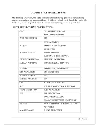
  • 1. 39 | P a g e CHAPTER-10 PCB MANUFACTURING After finishing CAM work, the FILES will send for manufacturing process. In manufacturing process, the manufacturing steps are different for different printed circuit board .like single side, double side, multisided pcb but the most common manufacturing process is given below. 10.1 PCB MANUFATURING PROCESS STEPS:- CNC CCL CUTTING,PINNING, STACKING&DRILLING WET PROCESSING DPS PIT (D/F) D/F LAMINATION EXPOSE & DEVELOPING WET PROCESSING CU PLATING RESIST STRIPPING ELECTING & TIN STRIPPING ETCHINGINSPECTION ETECHING INSPECTION SCREAN PRINTING BRUSHING & S/M PRINTING PIT(SM) EXPOSE (S/M), DEVELOPING S M INSPECTION S/M INSPECTION WET PROCESSING HAL SCREEN PRINTING L P CNC V-GROOVE & ROUTING BBT FIXURE FABRICATION & TESTING FINAL INSPECTION PCB INSPECTION PPE PRE PRODUCTION ENGINNERING,(DATA, FILMS,PANALISATION, CAM WORK ) STORES RAW MATERIALS &GENERAL STORE ACTIVITIES MANITENANCE PLANT MAINTENCE
  • 2. 40 | P a g e 10.1 Process Sequences for Single, Double and Multi-layer PCB Single side PCB Double side PCB Multi layer PCB File inspection File inspection File inspection Drill data generation Drill data generation Drill data generation Cutting Cutting Cutting Drilling Drilling I/L Tooling Holes Photo imaging DPS I/L Photo image Etching Photo imaging I/L Etching Solder masking PTH Oxide Treatment HASL Etching Pressing Legend print Solder Masking Drilling V-grooving / routing HASL De smear BBT Legend print DPS FQC V-grooving / routing Photo image Stores BBT PTH FQC Etching Stores Solder masking HASL Legend Printing V-grooving / routing BBT FQC Stores
  • 3. 41 | P a g e CHAPTER – 11 MANUFACTURING PROCESS 11.1 THE STEPS INVOLVED IN MANUFACTURING OF PRINTED CIRCUIT BOARD ARE:- 1) Pre production engineering:- In this process , two steps are involved they are file inspection and drill data generation, the engineers will generate through software called CAM work zone. As we explained in above chapter. the engineer will generate Circuit films, Solder Masking films, Legend Printing films at photo lab. Later these generated films are taken for production. Before the board is manufactured in the photo lab the circuit films, SM films, LP films are generated. It is called the pre production engineering.  The customer gives the original circuit and it is transferred on to the sheet in the photo lab process i.e. pre-production engineering. After the tasks are completed in photo lab then the film is taken for the exposing. Fig3.1.a photo lab DIAZO EXPOSING  For circuit we use diazo film.  The master film and diazo film are put in emulsion to emulsion contact in the exposure and the exposure is turned on.  The exposed diazo film is developed in the developer machine by bringing the emulsion in contact with ammonia vapour, and then films are developed.  Developed films are inspected and given for working to PIT.
  • 4. 42 | P a g e LITH EXPOSING  For SM and LP we use lith films.If the originals are negatives take positive copy.  The master film and lith film are put in emulsion to emulsion contact in the exposure and the exposure is turned on.  The exposed lith film is developed in the developer machine by bringing the emulsion in contact with developer solution, and then films are developed.  Developed films are inspected and given for working.Inspect SM films are given to PIT. 2) CNC computer numberical counter:-  In the first manufacturing step of CNC(computer numberical counter ) , the materials required are copper clade laminate, aluminum entry sheet, white tapes ,drill and router bits, emery paper, smooth files.  In this process we have using equipments like power sharing, stack master, wood backend, banioun waste, cotton gloves, tooth brush, DNC(data numerical counter), CNC driller(posalux), laminate, drill bits and router bits, aluminum entry sheets , backup and white tapes, emery paper, bunion waste, cotton gloves, smooth files, tooth brush, HSR drill bits.  In CNC process, CCL (copper clad laminate) is have to made into over customer required size. CCL MANUFACTURING:-
  • 5. 43 | P a g e  CCL has made up of chemical components which are resin and solvent both are compounding with each other because to make material hard. Now this chemical compounding will attach with glass cloth by the help of impregnation and drying now the chemical compounding becomes sheeting. This sheeting have to do pre-preg. Now pre- preg have to make ply-up. Now this whole process is known as “glass epoxy”.  Now this glass epoxy and copper/iron(cu/f) has combined with each other as over required.  For example there is 3 types of single side,double side, multi-side pcb. So as over required for single side pcb , we have to combine one side with glass epoxy and other side with copper or iron.  Same to double side and multi side pcbs .  i.e for double side PCB, glass epoxy and around copper /iron coating . whereas multi layer pcb is differ from others.  For multi layer pcb, they have to arrange one after another, first they arrange glass epoxy then coated with copper then again epoxy, as process repeat as over requirement.  Maximum 38 layers have done upto now . construction of layers will be depends upon thickness of copper . Fig. copper claded laminate with dimensions of 1245x1092 rectangle shape.  Glass epoxy has thickness of 0.2,0.4,0.6,0.8,1,1.2,1.6,2.4,3.2 mm. thickness is measure in microns.
  • 6. 44 | P a g e  Copper has thickness of standard sizes they are  Single side pcbs have a standard thickness of pcb board they are  1/0  35 microns  2/0  70 microns  Glass epoxy thickness of single side pcb is 0.8,1,1.6,1.2 mm.  For double side and multi side pcbs , thickness of the standard sizes of CCL sheet . o Length 1042x1245width o 1245x1092 o 1245x1042 o 1245x942  This sheet is packed with 10 nos and make a bandle.  Now customer will given circuit which sheet size is L2.03X110.29B now wander will plane how to generate required size of pcb.  Let us take an example as 1245x1042 sheet ,thickness of 1.6microns , this 1245x1042 sheet will cut sizes of L230X5=1150 and width w 250x4=1000. Remaining sheet is removed. Customer designed circuit size is 2.03x110.29, this will arrange the ciruit with more number of circuit on same boarded. So that 4 panel will be necessary in 230x48 board.This CCL sheet is cutted with the help of POWER SHARING which consists of blades with fixed sizes.  Now this sheet is send to “PINING”  Now other materials like backend sheet,aluminum entry sheet are also cutted in fixed sizes . this are used at the time of drilling .  H/H  17.5 microns  1/1  35 microns  2/2  70 microns
  • 7. 45 | P a g e Fig. power sharing with cutting of CCL PINING:-(22-8-14 to 30-8-14)  After receving from cutting , now the sheet is pining with the help of STACK MASTER (barnaby) which consist of drill bit with standard size of 3mm in this company.  This machine pins on both sides . STACKING:-  In stacking process, the panels have to arrange in a one bundle because while drilling, to reduce the power consumption and time, we have to make this stcking process.  Stacking will be depends upon thickness of board, i.e for example  1.6 mm  4panels can arrange in one bundle  2.4mm  2  0.8  5  1  5  Aluminum entry sheet is used because the copper boared will be damaged during the process of drilling , so aluminu entry sheet is used as a protection to the panel board.  Backend is used because will drilling the panels are shacking, so that damage will occurs , to avoid such damages, backend is used.With this both aluminum sheet and backend attach with bundles ,then send to drilling process.
  • 8. 46 | P a g e DRILLING PROCESS:-  During drilling process, different industries use diff drilling process but at sulakshana ciruit used specification drilling machines name called “POSALUX”, which has capable of drilling spindles no -8 and it will runs with a posalux software. After generating code for posalux, they insert a code to posalux software, posalux language is EXTELLOL .  Pre production engineer will generate this code with the help of CAD work. After inserting code to posalux, spindles starting working , before starting we have to insert the drills to spindles. the drillers sizes will be starts from 0.3mm to 6.5mm.  After inserting code and drillers, the work will starts and finished with required time.  If any errors detected, automatically system will stops and after finishing error correction by manually, the system work continuously. This is the process how to manufacture and materials required at CNC. After this process, the boared is send to wet processing. Fig posalux drilling machine with excellon software for viewer.
  • 9. 47 | P a g e 3) Direct plating system DPS(wet processing):-  It is the second step in the printed circuit board manufacturing.It is a direct plating system.It is an electroless copper deposition. It is a chemical bath .There will be a various combination of chemicals called shipyard chemicals.  Before processing of this stage the holes are not conductive. After the completion of this stage the holes are covered with palladium to make it conductive.  In this process we required to converting the insulated material into a conducting material by doing some electro less process. See in below fig.  That means “palladium material” is forming the conductive layer on the surface of the insulator. Fig.showing ship yard chemicall which boared is dumbed in this bunks for various times.  In direct plating system, the materials used in ship yard chemicals are sensitizer 5100B, sensitizer 5123M,activator 5300R, activator 5300B,enchancer 5400,stabilizer 5600,microtech 5700A,microtech 5700B,Sulphuric acid, hydrogen peroxide etc. they are different chemical have to used it depends upon customer required.
  • 10. 48 | P a g e 4) Photo image transform PIT(D/F):- In this process, it is important step in manufacturing process because transfer the image from art work inspected and issued by the photo lab. Photo imaging process is done in three stages. I. lamination , II. Exposing , III. Developing I. Lamination:-The whole board surface is laminated with a thin layer of photosensitive/etch resist (Photo Polymer Film) either by a liquid process or as a film. II. Exposing: - This resist layer is exposed to ultra-violet light through a photo tool (art work), so that the uncovered area is polymerized and hardened. Unhardened photo resist is removed by developing. The most commonly used phot resists are ‘negative’-working, which means they polymerize on exposure with ultraviolet light and hence become insoluble in a direct developer. Non-polymerized resist is removed by ‘developing’ to expose copper areas ready for electroplating. Fig showing laminating thin layer on board with help of achine and stacking the another thin layer for exposing and checking the circuit with drilles.
  • 11. 49 | P a g e . Fig exposing the dry film with machine which uv light exposing to boared. III. Developing:-In the developing process the non-polymerized film is soluble in the developing solution at certain concentration, pressure and speed of the conveyor. Then the boards are rinsed with water and dried in the dryer is given below. dry film is removed and washed with water and chemicals. Fig after exposing, the board is look like this and next step is drying with dryer.  The Mylar or dry film which protected the photo resist is now removed and the panel is moved out of the clean room and through a developer which removes the unhardened resist. For inner layers the copper pattern we want was covered by the resist. For outer layers it is exposed ready to be plated. The panels should have the copper surface is clean and all the unwanted resist has been removed. After finishing , the board is send to electro plating at wet processing.
  • 12. 50 | P a g e 5) Electro plating at wet processing or copper plating:-  In this we electrolyte the boards with copper .The operator loads the panels on the flight bars. Here we check for all the clamps to ensure good electric connection and a thin layer of tin is added. The panels themselves act as cathode for electro plating. Next we electroplate the boards with copper. The operator loads the panels onto the flight bars. He checks all the clamps to ensure a good electrical connection. The panels themselves act as cathodes for electroplating and we can plate the hole walls thanks to the conductive carbon layer already deposited there. The operator starts the automated plating line. The copper surface of the panels is cleaned and activated in a number of baths and then electroplated.  The whole process is computer controlled to ensure that each set or flight of panels stays in each bath exactly the right amount of time. You can see the copper anodes in their bags.  To ensure good conductivity through the holes we need to plate an average of 25 microns of copper on the hole walls. This means that we also plate 25 – 30 microns on the surface tracks. So if we start with a typical 17.5 micron copper foil it will be 40 – 42 microns after processing.  The baths are designed to produce an even copper thickness across the panel. Modern chemical solutions also have good “throwing power” to produce an even thickness of copper right through the hole.  Once we have plated the copper onto the board we then plate a thin layer of tin. This we will use in the next step of the process when we etch off the unwanted copper foil. Fig shows electro plating in which copper plating and tin plating.
  • 13. 51 | P a g e Fig shows the etching the unwanted material on bored by ship yard chemicals.  In simple word, in process we have to do “ electro plating system”. In this copper anode is present , sheet is presented in this copper is deposited on the board. After this ,Resist tripping have done acid base neutralization will done. After this the board is send to electing where it remove the unwanted copper. Then tin stripping where only tin is exposed.  After finishing electro plating , the board is send to etching inspection. Fig shows after finshing electro plating the boared become like this.
  • 14. 52 | P a g e 6) Etching inspection:-Where they detected the errors in board and send to next process or if errors are more they remove the board. In this process, basically inspection may be two types 1) manual optical inseption. 2) automatic optical inseption.  Automated optical inspection (AOI) is an automated visual inspection of a wide range of products, such as PCBs, LCDs, transistors, automotive parts, lids and labels on product packages .In case of PCB-inspection, a camera autonomously scans the device under test (DUT) for variety of surface feature defects such as scratches and stains, open circuits, short circuits, thinning of the solder as well as missing components, incorrect components, and incorrectly placed components.  Manual optical inspection(MOI) is a manual visual inspection range of products, such as PCBs, LCDs, transistors, automotive parts, lids and labels on product packages or agricultural products (seed corn or fruits). In pcb inspection man can be done through the help of light brightness and zooming mirror.  Errors deteting during inspection are as follows a. Line width violations. b. Spacing violation. c. Excess copper. d. Missing pad. (e.g. a feature that should be on the board is missing.) e. Short circuits. f. Cuts/Open circuits. g. Whole breakage.  These are errors detecting during manual optical inspection. But where as auto optical inspection there are few more errors detected by machines they are  Area Defects,  Billboarding  Component offset  Component polarity  Component presence/absence  Component skew  Excessive solder joints
  • 15. 53 | P a g e  Flipped component  Height Defects  Insufficient paste around Leads  Insufficient solder joints  Lifted leads  No-population tests  Paste registration  Severely damaged components  Solder bridges  Tombstoning  Volume defects  Wrong part. This error will done in all inspections like Etching inspection, soldermasking inspection, final inspection. Where they detected the errors in board and send to next process or if errors are more they remove the board. Fig show inpection in brightness if errors came, they detect and clear it with some technical equipment.
  • 16. 54 | P a g e 7) Screen printing:-  There are two tasks involved in it .They are brushing and S/M printing. Brushing is to remove roughness (or) to make the material smooth.  After brushing, we apply solder masking. We have epoxy ink solder mask on to each side of the board to protect the copper surface and prevent solder shorting between the components during assembly.  The electra glasses are used for the ink purpose in the manufacturing of printed circuit boards. fig show screen printing machine , board will be placed in middle part of machine pour ink.  EPOXY INK: It is the ink that is used to transfer the image on to the board. The colour of the ink is of different types. It depends on the customer specification, normally green colour is used.  They are acetone, brown tape, chromline, electra dark glass, electra light glass, electra black glass, rubber gloves, paper tape, soap oil, bleaching powder are materials required at screen printing.  After finishing screen printing, the board is send to heat the boards in over up to 70 degrees and cool them.
  • 17. 55 | P a g e 8) PIT photo image transfer (Solder Masking):- after completion of screen printing the ink is present in the holes of board to make the holes open. we use this method.we develop the boards using uv light, to observe whether all holes are open, are there are any short circuits.  Most boards have a epoxy-ink solder mask printed onto each side to protect the copper surface and prevent solder shorting between components during assembly  The panels are first cleaned and brushed to remove any surface tarnish. Each panel is given a final clean to remove any dust from the surface and loaded into the vertical coater. The coating machine simultaneously covers both sides of the panel with the epoxy solder mask ink. The double action ensures that the ink completely encapsulates the copper tracking, typically now 35 – 40 microns higher than the surface of the panel. fig solder mask epoxy ink.  The panels are now racked and put through a drier which hardens the resist just enough to allow it to be printed (“tack-dried”).  Next the coated panels are imaged. For this we use a two drawer UV printer. The operator mounts the photo tool films on the machine and then places the panel onto the registration pins.  The other areas which are not to be solderable are covered with a solder resist material. It is basically a polymer coating that prevents the solder from bringing traces and possibly creating shortcuts to nearby component leads.
  • 18. 56 | P a g e  The imaged panels are put out of the clean room and into the developer which strips off the unhardened and unwanted resist. Later the required resist will be further hardened or “cured” to provide a robust and permanent coat.  It is exposing and developing of a board, after the image is transferred on to the board using an ink called epoxy ink. Normally we use green colour. After solder masking we heat the boards in oven up to 70 degrees and cool them. Later we develop the boards using uv light, to observe whether all holes are open. Fig solder mask pcb heated and cooled  After finishing, this boared is send to sm inspection. 9) SM INSPECTION:-  It is to inspect the boards, whether all holes are open (or) any short circuits. 10)HOT AIR LEAVLING:-  The printed circuit board is dipped in to a bath of molten solder so that all the exposed copper surface is covered by solder. Excess solder is removed by passing the printed circuit board between hot air and knives. Fig show HAL , dipp the pcb in machine and after leveing hot air is leved out side see above.
  • 19. 57 | P a g e  Advantages of HAL are: Excellent wetting during component soldering.  Disadvantages of HAL are: High thermal stress during process may introduce the defects in printed circuit board. 10) Legend printing:-  In this process we have to print the colour on the component identification purpose. So that we used this process. We can print with white or red or other colours as our required with the help of machine. The machine is similar to screen printing machine as given in above page. Fig after legend printing, the board looks like this with this we can identify components placement.  After finishing legend printing, the PCB board is send to heat the boards in over up to 70 degrees and cool them. So that the board become hard. 11) CNC V-GROOVING AND ROUTING  These are used for creating break away tabs (or) lines. Routing builds a preceding step called placement which determines the location of each active element of an IC (or) component on printed circuit board.  After placement, the routing step adds wires needed to properly connects the placed components.
  • 20. 58 | P a g e ROUTING PROCESS  It is a step in which the board is shaped as per as customer requirement for the placement of the components. After component placement, the most important stage of the PCB design process is routing the connections.  for customer required we have to desired the boarded with shaped with the help of electronic machine.  The routing file is received from the photo lab is inserted in the machine with customer required. Fig shown that routing the shall of pcbs with posalux machine by the help of excellon file. V –GROVVING PROCESS  It is process, the machine will just drawn the cutting shape on the PCB board for cutting the board into small sized pcb as required. After this, the pcb is send to routing process.
  • 21. 59 | P a g e 12) Bare boared testing BBT :-  It is a bear board testing .It is used for the checking of errors in the printed circuit board. If there are any errors the board will be rejected and it will be indicated in the monitor screen.  The fixure fabrication & testing where we have to test the boared whether it is work or not with the help of machines. Fig show pcb is testing with the help of machines.  It is an Auto optimization inseption, which mean it can check with the board is working correctly or not. It will detect the errors as I mentioned in etching inseption. If more errors the board will be cancelled. 13) FINAL INSEPTION.  It is the last step in the printed circuit board manufacturing process. It is a manual optical inseption.can is done with man.  To check whether all the boards are perfect without any errors. If error is found the boards are rejected. If the boards are perfect the board is make into required customer size and then packed given to the customer in a given period of time.  After bear board testing i.e. Once again manually the boards are inspected to find errors i.e. whether the circuit is correct, any short circuits, and improper connections….etc.
  • 22. 60 | P a g e 14) Stores & manufacturing :-  In this process, they have to pack the product and make the payment and deliver to the customer. fig shown final packege of pcb.  With this manufactureing process is finished. Same process is repet for all boards like single side, double side, multi layer PCBs.  Next step is send to customer, there company they have to placement the component as per position in pcb and required wires and external protection layer is connected and tested the device whether it is working or not.
  • 23. 61 | P a g e CHAPTER -12 MARKETING MANAGEMENT IN PCB 12.1 Supply chain management We have learned about the Supply chain management Supply chain management place a crucial role in industry because it provides a great deal of interaction and trust between companies to work it provides an over site of materials information and finances as they move in suppler to the manufacturer to wholesaler to retailer to customer. It involves the coordinating and integrating these flows both within and among the companies.  12.2 COMPONENTS OF SUPPLY CHAIN MANAGEMENT Five basic components of Supply chain management are:   Planning: It is strategic portion of Supply chain management .In this companies need a strategy for managing all the resources.   Source: In this the companies must choose suppliers to deliver the goods and services that they need to create their product   Making/manufacturing: It is the manufacturing step. The company managers schedule the activities necessary for production, testing, packing and preparation for delivery.   Deliver: In this step the company coordinates the receipt of orders from customers pick carriers to get products to customers.   Return: In this step the supply chain planners (or) company managers to create responsive and flexible network for receiving defective and excess products back from customers and to support customers if they have any problem with the product. 
  • 24. 62 | P a g e 12.3 IDEAS OF SUPPLY CHAIN MANAGEMENT It is based on the two core ideas they are:  Practically every product that reaches an end user represents the cumulative effect of multiple organizations are referred to collectively as supply chain. While supply chains have existed for a long time most organizations have paid attention to what was happening with in their “four walls”. Supply chain management (SCM) is "the systemic, strategic coordination of the traditional business functions and the tactics across these business functions within a particular company and across businesses within the supply chain, for the purposes of improving the long term performance of the individual companies and the supply chain as a whole." It has also been defined as the "design, planning, execution, control, and monitoring of supply chain activities with the objective of creating net value, building a competitive infrastructure, leveraging worldwide logistics, synchronizing supply with demand and measuring performance globally."Supply chain management provides the oversight of materials, information, finances as they move from supplier to manufacturer to whole seller to retailer to customer.It involves the coordinating and integrating these flows both within and among companies. It is said that the ultimate goal of any effective supply chain management is to reduce the costs. Fig 5.3.a chain of supply chain management
  • 25. 63 | P a g e CHAPTER – 13 PCB marketing in world . 13.1 Pcb market size:-  Indian PCB Market Size, Imports INR 2650  Imports come mainly from China, Taiwan, Hong Kong, Korea and the US.  The import prices are almost at par with domestic prices with difference narrowing down to just 5-8%. The imports are largely due to huge demand-supply gap. However, domestic prices in medium volumes are competitive and do notface any threat from imports.  Exports INR 400 India is exporting about 24 percent of its production to the US, Germany, Malaysia, Austria, Belgium,Netherlands, the UK, Italy, Spain, Thailand and New Zealand. India exports single-side, double-side, andmultilayer PCBs.  Domestic INR 1250PCB manufacturers in India mostly cater across electronics applications in India except motherboards,mobiles and high-end telecom equipment.  Total Indian PCB Market Size = INR 4000 crores 13.2 An impressive 17% CAGR growing PCB demand The market demand is expected to grow to over 45Mn SQM by 2014 from existing 17.7Mn SQM at a CAGR of 17%. • The market is fairly large and there is no dependence on single or few suppliers or customers. Linaks will be able to encash this opportunity in the Domestic market. I. Consumer Electronics (CE) 38350 II. IndustrialElectronics/Automation (IE) 1150 III. Computers and peripherals 780 IV. Comn.& Broadcast eqpt. 4250 V. Strategic Electronics (SE) 220 VI. Automotive Electronics (AE) 720 Total 45470 17.00%
  • 26. 64 | P a g e 13.3 PCB Demand The main demands for PCBs come from consumer, industrial, and automotive electronics markets, as well as from Power & telecommunications. • PCB manufacturers in India mostly caters to the small to medium volumes across all sectors. • The mobile phone, PC and communication technology sectors which are biggest consumers of PCBs still rely a lot on imports. 13.4 PCB Usage Practices in India
  • 27. 65 | P a g e Fig shows aggregated demand in different devices with consumers and types of pcbs used by different sectors .
  • 28. 66 | P a g e CHAPTER- 14 Optimization of materials in pcb 14.1 Optimization in pcb manufacturing • In the first manufacturing step of CNC (Computer numericalcounter) the materials required are laminate, drill bits, router bits, aluminum entry sheet, white tapes, emery paper, banioun waste, cotton gloves, tooth brush, smooth files. • In the CNC ,This materials are necessary to manufacture the pcb . so there is no scope to optimize or to remove of this materials because this materials are used for designing and manufacturing purpose . hence there is no possible way to optimization of materials but in this step we can reduce the power usage only. • In the wet processing ,Various chemicals are used such as copper sulphate, stannous sulphate , sulphuricacid, sodium carbonate. sensitizer 5100B, sensitizer 5123M,activator 5300R, activator 5300B,enchancer 5400,stabilizer 5600,microtech 5700A,microtech 5700B,Sulphuric acid, hydrogen peroxide..etc. • In the wet processing, we use different chemicals and different combinations of chemicals because customer required different type of chemical in their making purpose so they require purpose we are using different chemical . • Different chemicals and different combinations of chemicals called shipyard chemicals. • In this wet processing we can optimize the usage of chemicals .we are using different chemicals after using every chemical we can prevent for another purpose or using for further steps. Like that we can do there is utilization of chemicals with out wasting. • In PIT(Photo image transfer ), there is no scope to optimization of materials in manufacturing . • In SM and LP(solder masking and laser printing), we can print the screen with customer required cheimicals . here we can optimize the chemical with less quantity using the chemicals will mixing the solutions. • After finising V-grovving and Routing in CNC, the unwanted metal or board can be send to copper cladding laminate manufacturing process because it will do again making of ccl. • In etching or sm or final inseption , the unwanted board and remove board can used for ccl making .
  • 29. 67 | P a g e • In HAL (hot air leavel), we can reduce the air pressure level . • This is all possible ways to optimize the chemicals and materials in pcb manufacturing . • By optimizing , the cost of pcb board also influences or in other worlds TO OPTIMIZE THE MATERIALS IN PCB MANUFACTURING , IT EFFECTS TO MANUFACTURING COST SIMULATION. • Failure Mode and Effect Analysis (FMEA) is that tool. FMEA is a formal process of identifying all the ways a process or product can fail, and then determining how to reduce or eliminate them. • Overall Equipment Effectiveness (OEE) is a metric that includes throughput, availability and quality. It is a metric that allows organizations to view performance of assets in the factory. • Availability = operating time/planned production time • Throughput (run rate) = (total pieces/operating time) / planned cycle time. • Quality = TPY = (good pieces / total pieces) • Since statistically over 80% of components are placed with automated SMT equipment, we move our focus on those specific assets. There are 3 main elements to optimizing process performance in SMT equipment, and ensuring high OEE: 1) Ensuring maximum availability of assets by minimizing downtime 2) Ensuring high throughput by ensuring optimal machine efficiency 3) Ensuring high quality by monitoring placement quality real-time.
  • 30. 68 | P a g e 14.2 Optimization of errors in CAD and CAM Some of the techniques how to optimize the PCB.As the given bellow this are few steps given by ■ Minimizing capture pads Altera’s boards regularly use 18-mil to 20-mil capture pads on 9-mil to 10-mil drill diameters, respectively. ■ Removing all non-functional pads Altera recommends removing all NFPs for designs with high aspect ratio vias. Altera regularly uses 9-mil and 10-mil drills on 90-mil and 100-mil thick PCBs, respectively (an aspect ratio of 10:1). ■ Increasing anti-pad diameter Altera recommends using 40-mil to 50-mil anti-pad clearances. Altera boards have achieved good performance results with 40-mil and 50-mil anti-pad via designs. ■ Minimizing via stubs Altera recommends using stripline routing on layers near the opposite surface of where the signal enters the via to minimize stub lengthsAdding AC return vias adjacent to each signal via: Altera recommends adding ground vias placed within 35 mils center-to-center adjacent to each signal via for providing better AC return path. ■ Using back drilling to remove stubs when appropriate. Example of how optimization is applicable to automated drilling operations for PCB , which has potential reduction of cost of PCB manufacturing. Fig Automated drilling operations for PCB.
  • 31. 69 | P a g e CHAPTER -15 Applications of PCB 15.1 Applications of PCB in electronic industries:  Applications in varied areas  Large and small  Rigid and flexible  Conventional electronics driver circuits like as below  Computerized Reflow Oven  Stencil Printer  Digital Oscilloscopes  Soldering Station  Multiple power supply  Frequency Generator  Multi Meter  Variact  EPROM Programmer.
  • 32. 70 | P a g e CHAPTER -16 RESULTS OF PROJECT. I had done project which results are given below. The results of CAD,CAM,FINAL PCB. 16.1 Result of CAD and CAM: Fig show circuit diagram for CAM schematic editor. Fig show result tracks of CAD.
  • 33. 71 | P a g e Figure shows CAM files of drilling files,routing,solder masking,legend printing and dry filmPIT. Fig show final pcb after manufacturing.
  • 34. 72 | P a g e Conclusion Optimization of materials and optimization in size reducing and error detection play a crucial role in printed circuit board. To reduce the size of pcb’s the current materials should be replaced by alternative materials .So that the size of pcb’s is reduced and cost of pcb’s is also reduced. There are many raw materials are used in the printed circuit board. As the size of printed circuit board plays a crucial role in today’s electronic industry. The main aim of the industry to supply the goods to the customer in a time limit. So in order meet target they should follow the supply chain management .Supply chain management gives the oversight of different departments together and coordinates them to meet the demand. Printed circuit boards (PCB) are one of the most important parts of electrical and electronic devices. It provides mechanical support for the electronic components. It interconnects the components to each other and provides input/output connections so that the electronics can interact with the user. PCBs are used in both desktop and laptop computers. They serve as the foundation for many internal computer components, such as video cards, controller cards, network interface cards, and expansion cards. These components all connect to the motherboard, which is also a printed circuit board. So these raw materials plays most important role in pcb manufacturing So in detail study of these raw materials will helps us to create different sizes of pcb’s which in turn reduces the cost and time for manufacturing. As the size of printed circuit board is reducing gradually and reasons for its gradual decrease in size is of usage of raw materials. There are around 150 raw materials are used and these raw materials plays a crucial role in the reduction of size of printed circuit board. To optimize the reducing of errors we have to use manual optical inspection. The costs of printed circuit board also intern should be reduced and also time for the manufacturing of printed circuit board.
  • 35. 73 | P a g e References 1) http://www.engineersgarage.com/contribution/kicad-tutorial?page=5 2) Sulakshana ckt ltd for manufacturing process. 3) Achieving Optimal Manufacturing Flow using OEE (Part 4)January 2011 4) http://communities.mentor.com/mgcx/community/manufacturing_solutions) 5) Viewmate pentlogon for CAM work. 6) KIicad for CAD simulation. 7) www.wikipedia.com and www.google.co.in. 8) www.sclpcb.com.