SlideShare uma empresa Scribd logo
1 de 82
Semiconductor and 
optoelectronics 
Prof.V.Krishnakumar 
Professor and Head 
Department of Physics 
Periyar University 
Salem – 636 011 
India
Electricity 
• Electricity is the flow of electrons 
• Good conductors (copper) have easily released 
electrons that drift within the metal 
• Under influence of electric field, electrons flow in 
a current 
–magnitude of current depends on magnitude 
of voltage applied to circuit, and the 
resistance in the path of the circuit 
• Current flow governed by Ohm’s Law 
+ V = IR 
electron flow direction 
-
Electron Bands 
• Electrons circle nucleus in 
defined shells 
– K 2 electrons 
– L 8 electrons 
– M 18 electrons 
– N 32 electrons 
• Within each shell, electrons 
are further grouped into 
subshells 
– s 2 electrons 
– p 6 electrons 
– d 10 electrons 
– f 14 electrons 
• electrons are assigned to 
shells and subshells from 
inside out 
– Si has 14 electrons: 2 K, 8 L, 4 M 
10 
6 
2 
M shell 
K 
L 
d 
p 
s
Electronic Materials 
• The goal of electronic materials is to 
generate and control the flow of an 
electrical current. 
• Electronic materials include: 
1. Conductors: have low resistance which 
allows electrical current flow 
2. Insulators: have high resistance which 
suppresses electrical current flow 
3. Semiconductors: can allow or suppress 
electrical current flow
Conductors 
• Good conductors have low resistance so 
electrons flow through them with ease. 
• Best element conductors include: 
– Copper, silver, gold, aluminum, & nickel 
• Alloys are also good conductors: 
– Brass & steel 
• Good conductors can also be liquid: 
– Salt water
Conductor Atomic Structure 
• The atomic structure of 
good conductors usually 
includes only one 
electron in their outer 
shell. 
– It is called a valence 
electron. 
– It is easily striped from 
the atom, producing 
current flow. Copper Atom
Insulators 
• Insulators have a high resistance so 
current does not flow in them. 
• Good insulators include: 
– Glass, ceramic, plastics, & wood 
• Most insulators are compounds of several 
elements. 
• The atoms are tightly bound to one 
another so electrons are difficult to strip 
away for current flow.
Semiconductors 
• Semiconductors are materials that essentially 
can be conditioned to act as good 
conductors, or good insulators, or any thing in 
between. 
• Common elements such as carbon, silicon, 
and germanium are semiconductors. 
• Silicon is the best and most widely used 
semiconductor.
Semiconductor Valence Orbit 
• The main 
characteristic of a 
semiconductor 
element is that it has 
four electrons in its 
outer or valence 
orbit.
Crystal Lattice Structure 
• The unique capability of 
semiconductor atoms is 
their ability to link 
together to form a 
physical structure called 
a crystal lattice. 
• The atoms link together 
with one another 
sharing their outer 
electrons. 
• These links are called 
covalent bonds. 
2D Crystal Lattice Structure
3D Crystal Lattice Structure
Semiconductors can be Insulators 
• If the material is pure semiconductor material like 
silicon, the crystal lattice structure forms an excellent 
insulator since all the atoms are bound to one another 
and are not free for current flow. 
• Good insulating semiconductor material is referred to 
as intrinsic. 
• Since the outer valence electrons of each atom are 
tightly bound together with one another, the electrons 
are difficult to dislodge for current flow. 
• Silicon in this form is a great insulator. 
• Semiconductor material is often used as an insulator.
Doping 
• To make the semiconductor conduct 
electricity, other atoms called impurities must 
be added. 
• “Impurities” are different elements. 
• This process is called doping.
Semiconductors can be Conductors 
• An impurity, or element 
like arsenic, has 5 
valence electrons. 
• Adding arsenic (doping) 
will allow four of the 
arsenic valence 
electrons to bond with 
the neighboring silicon 
atoms. 
• The one electron left 
over for each arsenic 
atom becomes 
available to conduct 
current flow.
N-Type Semiconductor 
The silicon doped with 
extra electrons is 
called an “N type” 
semiconductor. 
“N” is for negative, 
which is the charge 
of an electron.
Resistance Effects of Doping 
• If you use lots of arsenic atoms for doping, 
there will be lots of extra electrons so the 
resistance of the material will be low and 
current will flow freely. 
• If you use only a few boron atoms, there 
will be fewer free electrons so the 
resistance will be high and less current will 
flow. 
• By controlling the doping amount, virtually 
any resistance can be achieved.
Current Flow in N-type Semiconductors 
• The DC voltage source has a 
positive terminal that attracts 
the free electrons in the 
semiconductor and pulls 
them away from their atoms 
leaving the atoms charged 
positively. 
• Electrons from the negative 
terminal of the supply enter 
the semiconductor material 
and are attracted by the 
positive charge of the atoms 
missing one of their 
electrons. 
• Current (electrons) flows from 
the positive terminal to the 
negative terminal.
Another Way to Dope 
• You can also dope a 
semiconductor material with an 
atom such as boron that has 
only 3 valence electrons. 
• The 3 electrons in the outer 
orbit do form covalent bonds 
with its neighboring 
semiconductor atoms as 
before. But one electron is 
missing from the bond. 
• This place where a fourth 
electron should be is referred 
to as a hole. 
• The hole assumes a positive 
charge so it can attract 
electrons from some other 
source. 
• Holes become a type of 
current carrier like the electron 
to support current flow.
P-Type Semiconductor 
Silicon doped with 
material missing 
electrons that produce 
locations called holes 
is called “P type” 
semiconductor. 
“P” is for positive, 
which is the charge 
of a hole.
Current Flow in P-type Semiconductors 
• Electrons from the negative 
supply terminal are attracted 
to the positive holes and fill 
them. 
• The positive terminal of the 
supply pulls the electrons 
from the holes leaving the 
holes to attract more 
electrons. 
• Current (electrons) flows from 
the negative terminal to the 
positive terminal. 
• Inside the semiconductor 
current flow is actually by the 
movement of the holes from 
positive to negative.
Introduction to Semiconductor Devices 
Semiconductor p-n junction diodes 
p 
n
p-n junction formation 
p-type material 
Semiconductor material 
doped with acceptors. 
Material has high hole 
concentration 
Concentration of free 
electrons in p-type material 
is very low. 
n-type material 
Semiconductor material 
doped with donors. 
Material has high 
concentration of free 
electrons. 
Concentration of holes in 
n-type material is very 
low.
p-n junction formation 
p-type material 
Contains 
NEGATIVELY 
charged acceptors 
(immovable) and 
POSITIVELY charged 
holes (free). 
Total charge = 0 
n-type material 
Contains 
POSITIVELY charged 
donors (immovable) 
and NEGATIVELY 
charged free electrons. 
Total charge = 0
Diffusion 
A substance, the purple dots, in 
solution. A membrane prevents 
movement of the water and the 
molecules from crossing from 
one side of the beaker to the 
other. 
Now that the gates have been 
opened, the random movements of 
the molecules have caused, 
overtime, the number of molecules 
to be equal on the two sides of the 
barrier.
Diffusion 
As a result of diffusion, the molecules or other free 
particles distribute uniformly over the entire volume
p- n junction formation 
What happens if n- and p-type materials are in close contact? 
Being free particles, electrons start diffusing from n-type material into p-material 
Being free particles, holes, too, start diffusing from p-type material into n-material 
Have they been NEUTRAL particles, eventually all the free electrons 
and holes had uniformly distributed over the entire compound crystal. 
However, every electrons transfers a negative charge (-q) onto the p-side 
and also leaves an uncompensated (+q) charge of the donor on 
the n-side. 
Every hole creates one positive charge (q) on the n-side and (-q) on 
the p-side
p- n junction formation 
What happens if n- and p-type materials are in close contact? 
p-type n-type 
Electrons and holes remain staying close to the p-n junction because 
negative and positive charges attract each other. 
Negative charge stops electrons from further diffusion 
Positive charge stops holes from further diffusion 
The diffusion forms a dipole charge layer at the p-n junction interface. 
There is a “built-in” VOLTAGE at the p-n junction interface that prevents 
penetration of electrons into the p-side and holes into the n-side.
p- n junction current – voltage characteristics 
What happens when the voltage is applied to a p-n junction? 
p-type n-type 
The polarity shown, attracts holes to the left and electrons to the right. 
According to the current continuity law, the current can only flow if 
all the charged particles move forming a closed loop 
However, there are very few holes in n-type material and there are 
very few electrons in the p-type material. 
There are very few carriers available to support the current through 
the junction plane 
For the voltage polarity shown, the current is nearly zero
p- n junction current – voltage characteristics 
What happens if voltage of opposite polarity is applied to a p-n junction? 
p-type n-type 
The polarity shown, attracts electrons to the left and holes to the right. 
There are plenty of electrons in the n-type material and plenty of holes 
in the p-type material. 
There are a lot of carriers available to cross the junction. 
When the voltage applied is lower than the built-in voltage, 
the current is still nearly zero 
When the voltage exceeds the built-in voltage, the current can flow through 
the p-n junction
Diode current – voltage (I-V) characteristics 
Semiconductor diode consists of a p-n junction with two 
contacts attached to the p- and n- sides 
V 0 
ù 
p n 
I I qV S exp 
= æ 1 
úû 
é 
êë 
ö çè 
- ÷ø 
kT 
IS is usually a very small current, IS ≈ 10-17 …10-13 A 
When the voltage V is negative (“reverse” polarity) the exponential term ≈ -1; 
The diode current is ≈ IS ( very small). 
When the voltage V is positive (“forward” polarity) the exponential term 
increases rapidly with V and the current is high.
p- n diode applications: 
Light emitters 
P-n junction can emit the 
light when forward biased 
p-type n-type 
+- 
Electrons drift into p-material and find plenty of holes there. They 
“RECOMBINE” by filling up the “empty” positions. 
Holes drift into n-material and find plenty of electrons there. They also 
“RECOMBINE” by filling up the “empty” positions. 
The energy released in the process of “annihilation” produces 
PHOTONS – the particles of light
+- 
p- n diode applications: 
Photodetectors 
P-n junction can detect light 
when reverse biased 
p-type n-type 
When the light illuminates the p-n junction, the photons energy RELEASES free 
electrons and holes. 
They are referred to as PHOTO-ELECTRONS and PHOTO-HOLES 
The applied voltage separates the photo-carriers attracting electrons toward 
“plus” and holes toward “minus” 
As long as the light is ON, there is a current flowing through the p-n junction
CB 
VB 
WWhheenn tthhee eelleeccttrroonn 
ffaallllss ddoowwnn ffrroomm 
ccoonndduuccttiioonn bbaanndd aanndd 
ffiillllss iinn aa hhoollee iinn 
vvaalleennccee bbaanndd,, tthheerree iiss 
aann oobbvviioouuss lloossss ooff 
eenneerrggyy..
IInn oorrddeerr ttoo aacchhiieevvee aa 
rreeaassoonnaabbllee eeffffiicciieennccyy 
ffoorr pphhoottoonn eemmiissssiioonn,, 
tthhee sseemmiiccoonndduuccttoorr 
mmuusstt hhaavvee aa ddiirreecctt 
bbaanndd ggaapp.. 
CB 
VB
FFoorr eexxaammppllee;; 
SSiilliiccoonn iiss kknnoowwnn aass aann iinnddiirreecctt bbaanndd--ggaapp 
mmaatteerriiaall.. 
aass aann eelleeccttrroonn ggooeess ffrroomm tthhee bboottttoomm ooff 
tthhee ccoonndduuccttiioonn bbaanndd ttoo tthhee ttoopp ooff tthhee 
vvaalleennccee bbaanndd;; 
iitt mmuusstt aallssoo uunnddeerrggoo aa 
ssiiggnniiffiiccaanntt cchhaannggee iinn 
mmoommeennttuumm.. 
CB 
VB 
WWhhaatt tthhiiss mmeeaannss iiss tthhaatt 
E 
k
• As we all kknnooww,, wwhheenneevveerr ssoommeetthhiinngg cchhaannggeess 
ssttaattee,, oonnee mmuusstt ccoonnsseerrvvee nnoott oonnllyy eenneerrggyy,, bbuutt 
aallssoo mmoommeennttuumm.. 
• IInn tthhee ccaassee ooff aann eelleeccttrroonn ggooiinngg ffrroomm 
ccoonndduuccttiioonn bbaanndd ttoo tthhee vvaalleennccee bbaanndd iinn ssiilliiccoonn,, 
bbootthh ooff tthheessee tthhiinnggss ccaann oonnllyy bbee ccoonnsseerrvveedd:: 
The transition also creates a 
quantized set of lattice vibrations, 
called phonons, or "heat“ .
• PPhhoonnoonnss ppoosssseessss bbootthh eenneerrggyy aanndd mmoommeennttuumm.. 
• TThheeiirr ccrreeaattiioonn uuppoonn tthhee rreeccoommbbiinnaattiioonn ooff aann 
eelleeccttrroonn aanndd hhoollee aalllloowwss ffoorr ccoommpplleettee 
ccoonnsseerrvvaattiioonn ooff bbootthh eenneerrggyy aanndd mmoommeennttuumm.. 
• AAllll ooff tthhee eenneerrggyy wwhhiicchh tthhee eelleeccttrroonn ggiivveess uupp iinn 
ggooiinngg ffrroomm tthhee ccoonndduuccttiioonn bbaanndd ttoo tthhee vvaalleennccee 
bbaanndd ((11..11 eeVV)) eennddss uupp iinn pphhoonnoonnss,, wwhhiicchh iiss 
aannootthheerr wwaayy ooff ssaayyiinngg tthhaatt tthhee eelleeccttrroonn hheeaattss uupp 
tthhee ccrryyssttaall..
In aa ccllaassss ooff mmaatteerriiaallss ccaalllleedd ddiirreecctt bbaanndd--ggaapp 
sseemmiiccoonndduuccttoorrss;; 
»tthhee ttrraannssiittiioonn ffrroomm ccoonndduuccttiioonn bbaanndd ttoo 
vvaalleennccee bbaanndd iinnvvoollvveess eesssseennttiiaallllyy nnoo 
cchhaannggee iinn mmoommeennttuumm.. 
»PPhhoottoonnss,, iitt ttuurrnnss oouutt,, ppoosssseessss aa ffaaiirr 
aammoouunntt ooff eenneerrggyy (( sseevveerraall eeVV/pphhoottoonn 
iinn ssoommee ccaasseess )) bbuutt tthheeyy hhaavvee vveerryy 
lliittttllee mmoommeennttuumm aassssoocciiaatteedd wwiitthh 
tthheemm..
• Thus, for a ddiirreecctt bbaanndd ggaapp mmaatteerriiaall,, tthhee eexxcceessss 
eenneerrggyy ooff tthhee eelleeccttrroonn--hhoollee rreeccoommbbiinnaattiioonn ccaann 
eeiitthheerr bbee ttaakkeenn aawwaayy aass hheeaatt,, oorr mmoorree lliikkeellyy,, aass 
aa pphhoottoonn ooff lliigghhtt.. 
• TThhiiss rraaddiiaattiivvee ttrraannssiittiioonn tthheenn 
ccoonnsseerrvveess eenneerrggyy aanndd mmoommeennttuumm 
bbyy ggiivviinngg ooffff lliigghhtt wwhheenneevveerr aann 
eelleeccttrroonn aanndd hhoollee rreeccoommbbiinnee.. CB 
VB 
TThhiiss ggiivveess rriissee ttoo 
((ffoorr uuss)) aa nneeww ttyyppee 
ooff ddeevviiccee;; 
tthhee lliigghhtt eemmiittttiinngg ddiiooddee ((LLEEDD))..
What is LED? 
Semiconductors 
bring quality 
to light! 
LED are semiconductor p-n junctions that under forward bias conditions can emit 
radiation by electroluminescence in the UV, visible or infrared regions of the 
electromagnetic spectrum. The qaunta of light energy released is approximately 
proportional to the band gap of the semiconductor.
Getting to know LED 
Advantages of Light Emitting Diodes (LEDs) 
Longevity: 
The light emitting element in a diode is a small 
conductor chip rather than a filament which greatly 
extends the diode’s life in comparison to an 
incandescent bulb (10 000 hours life time compared 
to ~1000 hours for incandescence light bulb) 
Efficiency: 
Diodes emit almost no heat and run at very low 
amperes. 
Greater Light Intensity: 
Since each diode emits its own light 
Cost: 
Not too bad 
Robustness: 
Solid state component, not as fragile as 
incandescence light bulb
LED chip is the part 
that we shall deal 
with in this course
Luminescence is the process 
behind light emission 
• Luminescence is a term used to describe the 
emission of radiation from a solid when the 
solid is supplied with some form of energy. 
• Electroluminescence  excitation results 
from the application of an electric field 
• In a p-n junction diode injection 
electroluminescence occurs resulting in light 
emission when the junction is forward biased
PPrroodduucciinngg pphhoottoonn 
EElleeccttrroonnss rreeccoommbbiinnee wwiitthh hhoolleess.. 
EEnneerrggyy ooff pphhoottoonn iiss tthhee eenneerrggyy ooff 
bbaanndd ggaapp.. 
CB 
VB 
e-h
How does it work? 
P-n junction Electrical 
Contacts 
A typical LED needs aa pp--nn jjuunnccttiioonn 
There are a lot of electrons and holes at 
the junction due to excitations 
Electrons from n need to be injected to p 
to promote recombination 
Junction is biased to produce even more 
e-h and to inject electrons from n to p for 
recombination to happen 
Recombination 
produces light!!
Injection Luminescence in 
LED 
 Under forward bias – majority carriers from both sides of the junction 
can cross the depletion region and entering the material at the other 
side. 
 Upon entering, the majority carriers become minority carriers 
 For example, electrons in n-type (majority carriers) enter the p-type 
to become minority carriers 
 The minority carriers will be larger  minority carrier injection 
 Minority carriers will diffuse and recombine with the majority carrier. 
 For example, the electrons as minority carriers in the p-region will 
recombine with the holes. Holes are the majority carrier in the p-region. 
 The recombination causes light to be emitted 
 Such process is termed radiative recombination.
MMAATTEERRIIAALLSS FFOORR LLEEDDSS 
• TThhee sseemmiiccoonndduuccttoorr bbaannddggaapp 
eenneerrggyy ddeeffiinneess tthhee eenneerrggyy ooff tthhee 
eemmiitttteedd pphhoottoonnss iinn aa LLEEDD.. 
• TToo ffaabbrriiccaattee LLEEDDss tthhaatt ccaann eemmiitt 
pphhoottoonnss ffrroomm tthhee iinnffrraarreedd ttoo tthhee 
uullttrraavviioolleett ppaarrttss ooff tthhee ee..mm.. 
ssppeeccttrruumm,, tthheenn wwee mmuusstt ccoonnssiiddeerr 
sseevveerraall ddiiffffeerreenntt mmaatteerriiaall 
ssyysstteemmss.. 
• NNoo ssiinnggllee ssyysstteemm ccaann ssppaann tthhiiss 
eenneerrggyy bbaanndd aatt pprreesseenntt,, aalltthhoouugghh 
tthhee 33--55 nniittrriiddeess ccoommee cclloossee.. 
CB 
VB
• Unfortunately, many ooff ppootteennttiiaallllllyy uusseeffuull 22--66 
ggrroouupp ooff ddiirreecctt bbaanndd--ggaapp sseemmiiccoonndduuccttoorrss 
((ZZnnSSee,,ZZnnTTee,,eettcc..)) ccoommee nnaattuurraallllyy ddooppeedd eeiitthheerr pp-- 
ttyyppee,, oorr nn--ttyyppee,, bbuutt tthheeyy ddoonn’’tt lliikkee ttoo bbee ttyyppee-- 
ccoonnvveerrtteedd bbyy oovveerrddooppiinngg.. 
• TThhee mmaatteerriiaall rreeaassoonnss bbeehhiinndd tthhiiss aarree 
ccoommpplliiccaatteedd aanndd nnoott eennttiirreellyy wweellll--kknnoowwnn.. 
• TThhee ssaammee pprroobblleemm iiss eennccoouunntteerreedd iinn tthhee 33--55 
nniittrriiddeess aanndd tthheeiirr aallllooyyss IInnNN,, GGaaNN,, AAllNN,, IInnGGaaNN,, 
AAllGGaaNN,, aanndd IInnAAllGGaaNN.. TThhee aammaazziinngg tthhiinngg aabboouutt 
33--55 nniittrriiddee aallllooyy ssyysstteemmss iiss tthhaatt aappppeeaarr ttoo bbee 
ddiirreecctt ggaapp tthhrroouugghhoouutt..
Construction of Typical LED 
Light output 
n 
Substrate 
Al 
SiO2 
Electrical 
contacts 
p
LED Construction 
 Efficient light emitter is also an efficient absorbers of 
radiation therefore, a shallow p-n junction required. 
 Active materials (n and p) will be grown on a lattice 
matched substrate. 
 The p-n junction will be forward biased with contacts 
made by metallisation to the upper and lower surfaces. 
 Ought to leave the upper part ‘clear’ so photon can 
escape. 
 The silica provides passivation/device isolation and 
carrier confinement
Efficient LED 
 Need a p-n junction (preferably the same 
semiconductor material only different dopants) 
 Recombination must occur  Radiative 
transmission to give out the ‘right coloured LED’ 
 ‘Right coloured LED’  hc/l = Ec-Ev = Eg 
 so choose material with the right Eg 
 Direct band gap semiconductors to allow efficient 
recombination 
 All photons created must be able to leave the 
semiconductor 
 Little or no reabsorption of photons
Correct band gap Direct band gap 
Materials 
Requirements 
Material can be 
made p and n-type 
Efficient radiative 
pathways must exist
Direct band gap 
Candidate 
Materials 
materials 
e.g. GaAs not Si 
 UV-ED l ~0.5-400nm 
Eg > 3.25eV 
 LED - l ~450-650nm 
Eg = 3.1eV to 1.6eV 
 IR-ED- l ~750nm- 1nm 
Eg = 1.65eV 
Readily Materials with refractive doped n or p-types 
index that could allow light 
to ‘get out’
Candidate Materials 
Group III-V & Group II-VI 
Group II Group III Group IV Group V 
iii iv v 
ii 
Al 
Ga 
In 
N 
P 
As 
Periodic Table to show group III-V and II-V binaries
Candidate Materials 
Group III-V & Group II-VI 
Group II Group III Group IV Group V 
iii iv v 
ii 
Al 
Ga 
In 
N 
P 
As 
Periodic Table to show group III-V and II-V binaries
CCoolloorr NNaammee WWaavveelleennggtthh 
((NNaannoommeetteerrss)) 
SSeemmiiccoonndduuccttoorr 
CCoommppoossiittiioonn 
IInnffrraarreedd 888800 GGaaAAllAAss//GGaaAAss 
UUllttrraa RReedd 666600 GGaaAAllAAss//GGaaAAllAAss 
SSuuppeerr RReedd 663333 AAllGGaaIInnPP 
SSuuppeerr OOrraannggee 661122 AAllGGaaIInnPP 
OOrraannggee 660055 GGaaAAssPP//GGaaPP 
YYeellllooww 558855 GGaaAAssPP//GGaaPP 
IInnccaannddeesscceenntt 
WWhhiittee 44550000KK ((CCTT)) IInnGGaaNN//SSiiCC 
PPaallee WWhhiittee 66550000KK ((CCTT)) IInnGGaaNN//SSiiCC 
CCooooll WWhhiittee 88000000KK ((CCTT)) IInnGGaaNN//SSiiCC 
PPuurree GGrreeeenn 555555 GGaaPP//GGaaPP 
SSuuppeerr BBlluuee 447700 GGaaNN//SSiiCC 
BBlluuee VViioolleett 443300 GGaaNN//SSiiCC 
UUllttrraavviioolleett 339955 IInnGGaaNN//SSiiCC
Getting to know LED 
Advantages of Light Emitting Diodes (LEDs) 
Longevity: 
The light emitting element in a diode is a small 
conductor chip rather than a filament which greatly 
extends the diode’s life in comparison to an 
incandescent bulb (10 000 hours life time compared 
to ~1000 hours for incandescence light bulb) 
Efficiency: 
Diodes emit almost no heat and run at very low 
amperes. 
Greater Light Intensity: 
Since each diode emits its own light 
Cost: 
Not too bad 
Robustness: 
Solid state component, not as fragile as 
incandescence light bulb
LED chip is the part 
that we shall deal 
with in this course
Some Types of LEDs 
Bargraph 7-segment Starburst Dot matrix
Applications of LEDs
Your fancy telephone, i-pod, palm pilot 
and digital camera
• Diode laser
• What is the word LASER 
stands for? 
• Light amplification by Stimulated Emission of 
Radiation
Stimulated Emission 
E2 
E1 
hu 
(a) Absorption 
hu 
E2 E2 
E1 E1 
(b) Spontaneous emission 
hu 
In hu 
Out 
hu 
(c) Stimulated emission 
Absorption, spontaneous (random photon) emission and stimulated 
emission. 
© 1999 S.O. Kasap, Optoelectronics (Prentice Hall) 
In stimulated emission, an incoming photon with energy hu stimulates the 
emission process by inducing electrons in E2 to transit down to E1. 
While moving down to E1, photon of the same energy hu will be emitted 
Resulting in 2 photons coming out of the system 
Photons are amplified – one incoming photon resulting in two photons 
coming out.
Population Inversion 
• Non equilibrium distribution of 
atoms among the various 
energy level atomic system 
• To induce more atoms in E2, i.e. 
to create population inversion, 
a large amount of energy is 
required to excite atoms to E2 
• The excitation process of atoms 
so N2 > N2 is called pumping 
• It is difficult to attain pumping 
when using two-level-system. 
• Require 3-level system instead 
More atoms 
here 
E2 
E1 
N2> N1 
N2 
N1 
E3 
E2 
E1 
There level 
system
Principles of Laser 
E 
3 
E 
1 
hu13 
E 
2 
Metastable 
state 
E 
3 
E 
1 
E 
2 
hu32 
E 
3 
E 
1 
E 
2 
E 
3 
E 
1 
E 
2 
OUT 
hu21 
hu21 
Coherent photons 
(a) (b) (c) (d) 
. 
IN 
• In actual case, excite atoms from E1 to E3. 
• Exciting atoms from E1 to E3 optical pumping 
• Atoms from E3 decays rapidly to E2 emitting hu3 
• If E2 is a long lived state, atoms from E2 will not decay to E1 rapidly 
• Condition where there are a lot of atoms in E2 population inversion 
achieved! i.e. between E2 and E1.
Coherent Photons Production 
(explanation of (d)) 
• When one atom in E2 decays 
spontaneously, a random photon 
resulted which will induce stimulated 
photon from the neighbouring atoms 
• The photons from the neighbouring 
atoms will stimulate their neighbours 
and form avalanche of photons. 
• Large collection of coherent photons 
resulted.
Laser Diode Principle 
• Consider a p-n junction 
• In order to design a laser diode, the p-n junction must be 
heavily doped. 
• In other word, the p and n materials must be degenerately 
doped 
• By degenerated doping, the Fermi level of the n-side will lies in 
the conduction band whereas the Fermi level in the p-region 
will lie in the valance band.
Diode Laser Operation 
p+ n+ 
E 
Fn 
E 
g 
(a) 
E 
c 
E 
v 
E 
v 
Holes inVB 
Junction 
Electrons inCB 
Electrons E 
c 
p+ 
E 
g 
V 
n+ 
(b) 
E 
Fn 
eV 
E 
Fp 
Inversion 
region 
E 
Fp 
E 
c 
E 
c 
eV 
o 
•P-n junction must be degenerately doped. 
•Fermi level in valance band (p) and 
conduction band (n). 
•No bias, built n potential; eVo barrier to stop 
electron and holes movement 
•Forward bias, eV> Eg 
•Built in potential diminished to zero 
•Electrons and holes can diffuse to the space 
charge layer
Application of Forward Bias 
• Suppose that the degenerately doped p-n junction 
is forward biased by a voltage greater than the 
band gap; eV > Eg 
• The separation between EFn and EFp is now the 
applied potential energy 
• The applied voltage diminished the built-in 
potential barrier, eVo to almost zero. 
• Electrons can now flow to the p-side 
• Holes can now flow to the n-side
Population Inversion in Diode 
Laser 
hu 
Optical gain EFn - EFp 
Eg 
0 
Optical absorption 
Energy 
EFn 
Ec 
Ev 
CB 
VB 
Electrons 
in CB 
Holes in VB 
= Empty states 
Density of states 
EFp 
eV 
At T > 0 
At T = 0 
(a) (b) 
(a) The density of states and energy distribution of electrons and holes in 
the conduction and valence bands respectively at T » 0 in the SCL 
under forward bias such that EFn - EFp > Eg. Holes in the VB are empty 
states. (b) Gain vs. photon energy. 
© 1999 S.O. Kasap, Optoelectronics (Prentice Hall)
Population Inversion in Diode 
Laser 
Electrons in CB 
EFn 
EFp 
CB 
VB 
Eg 
Holes in VB 
eV 
EFn-EfP = eV 
eV > Eg 
eV = forward bias voltage 
Fwd Diode current pumping  
injection pumping 
More electrons in 
the conduction 
band near EC 
Than electrons in 
the valance band 
near EV 
There is therefore a population inversion between 
energies near EC and near EV around the junction. 
This only achieved when degenerately doped p-n 
junction is forward bias with energy > Egap
The Lasing Action 
• The population inversion region is a layer along the 
junction  also call inversion layer or active region 
• Now consider a photon with E = Eg 
• Obviously this photon can not excite electrons from 
EV since there is NO electrons there 
• However the photon CAN STIMULATE electron to 
fall down from CB to VB. 
• Therefore, the incoming photon stimulates 
emission than absorption 
• The active region is then said to have ‘optical gain’ 
since the incoming photon has the ability to cause 
emission rather than being absorbed.
Pumping Mechanism in 
Laser Diode 
• It is obvious that the population inversion 
between energies near EC and those near EV 
occurs by injection of large charge carrier 
across the junction by forward biasing the 
junction. 
• Therefore the pumping mechanism is 
FORWARD DIODE CURRENT  Injection 
pumping
For Successful Lasing Action: 
1. Optical Gain (not absorb) 
Achieved by population inversion 
2. Optical Feedback 
Achieved by device configuration 
Needed to increase the total optical amplification by making photons 
pass through the gain region multiple times 
Insert 2 mirrors at each end of laser 
This is term an oscillator cavity or Fabry Perot cavity 
Mirrors are partly transmitted and party reflected
Materials for Laser Diodes
Optical Power in Laser is Very 
High due to Optical Feedback and 
Higher Forward Bias Current. 
Threshold current density
Direct Gap Diode Laser 
• Direct band gap  high probability of electrons-holes 
recombination  radioactively 
• The recombination radiation may interact with the 
holes in the valance band and being absorbed or 
interact with the electrons in the conduction band 
thereby stimulating the production of further 
photons of the same frequency  stimulated 
emission
Materials 
Available
Technologically Important 
Material for Blue Laser
InGaN and AlGaN 
• InGaN and AlGaN have been produced over the entire composition 
range between their component binaries; InN, GaN, AlN 
• InAlN is less explored. 
• GaN and AlN are fairly well lattice-matched to SiC substrates, 
• SiC has substrate is better as it can be doped (dopability) and high 
thermal conductivity relative to more commonly used Al2O3 substrates. 
• AlN and GaN can be used for high temperature application due to 
wide bandgaps and low intrinsic carrier concentrations.
Laser sword

Mais conteúdo relacionado

Mais procurados

Ion Implantation
Ion Implantation Ion Implantation
Ion Implantation Younes Sina
 
PHOTONIC DEVICES INTRODUCTION
PHOTONIC DEVICES INTRODUCTIONPHOTONIC DEVICES INTRODUCTION
PHOTONIC DEVICES INTRODUCTIONAnkit Pandey
 
Transition metal dichalcogenide NPs, recent advances in scientific research
Transition metal dichalcogenide NPs, recent advances in scientific researchTransition metal dichalcogenide NPs, recent advances in scientific research
Transition metal dichalcogenide NPs, recent advances in scientific researchANJUNITHIKURUP
 
Fabrication of Semiconductors
Fabrication of SemiconductorsFabrication of Semiconductors
Fabrication of Semiconductorsaman1312
 
Non linear optics and SHG
Non linear optics and SHGNon linear optics and SHG
Non linear optics and SHGsahil rajput
 
Band structure(2)
Band structure(2)Band structure(2)
Band structure(2)David David
 
Resonant Tunneling Diodes
Resonant Tunneling DiodesResonant Tunneling Diodes
Resonant Tunneling Diodessanjeevstewart
 
Introduction to nanophotonics
Introduction to nanophotonicsIntroduction to nanophotonics
Introduction to nanophotonicsajayrampelli
 
Lecture 4 4521 semiconductor device physics - metal-semiconductor system
Lecture 4   4521 semiconductor device physics - metal-semiconductor systemLecture 4   4521 semiconductor device physics - metal-semiconductor system
Lecture 4 4521 semiconductor device physics - metal-semiconductor systemNedal Al Taradeh
 
Metal semiconductor contact
Metal semiconductor contactMetal semiconductor contact
Metal semiconductor contactAnchit Biswas
 
Opto electronics devices
Opto electronics devicesOpto electronics devices
Opto electronics devicesSiddharth Panda
 
Float Zone, Bridgman Techniques--ABU SYED KUET
Float Zone, Bridgman Techniques--ABU SYED KUETFloat Zone, Bridgman Techniques--ABU SYED KUET
Float Zone, Bridgman Techniques--ABU SYED KUETA. S. M. Jannatul Islam
 

Mais procurados (20)

Ion Implantation
Ion Implantation Ion Implantation
Ion Implantation
 
Nonlinear optics
Nonlinear opticsNonlinear optics
Nonlinear optics
 
PHOTONIC DEVICES INTRODUCTION
PHOTONIC DEVICES INTRODUCTIONPHOTONIC DEVICES INTRODUCTION
PHOTONIC DEVICES INTRODUCTION
 
Powerpoint slides
Powerpoint slidesPowerpoint slides
Powerpoint slides
 
non linear optics
non linear opticsnon linear optics
non linear optics
 
Transition metal dichalcogenide NPs, recent advances in scientific research
Transition metal dichalcogenide NPs, recent advances in scientific researchTransition metal dichalcogenide NPs, recent advances in scientific research
Transition metal dichalcogenide NPs, recent advances in scientific research
 
Fabrication of Semiconductors
Fabrication of SemiconductorsFabrication of Semiconductors
Fabrication of Semiconductors
 
Theory of surface plasmon polaritons
Theory of surface plasmon polaritonsTheory of surface plasmon polaritons
Theory of surface plasmon polaritons
 
Design of Thin Film Solar Cell
Design of Thin Film Solar CellDesign of Thin Film Solar Cell
Design of Thin Film Solar Cell
 
SEMICONDUCTOR PHYSICS
SEMICONDUCTOR PHYSICSSEMICONDUCTOR PHYSICS
SEMICONDUCTOR PHYSICS
 
Non linear optics and SHG
Non linear optics and SHGNon linear optics and SHG
Non linear optics and SHG
 
Photonic Crystals
Photonic CrystalsPhotonic Crystals
Photonic Crystals
 
Band structure(2)
Band structure(2)Band structure(2)
Band structure(2)
 
Resonant Tunneling Diodes
Resonant Tunneling DiodesResonant Tunneling Diodes
Resonant Tunneling Diodes
 
Introduction to nanophotonics
Introduction to nanophotonicsIntroduction to nanophotonics
Introduction to nanophotonics
 
Lecture 4 4521 semiconductor device physics - metal-semiconductor system
Lecture 4   4521 semiconductor device physics - metal-semiconductor systemLecture 4   4521 semiconductor device physics - metal-semiconductor system
Lecture 4 4521 semiconductor device physics - metal-semiconductor system
 
Metal semiconductor contact
Metal semiconductor contactMetal semiconductor contact
Metal semiconductor contact
 
Plasmons
PlasmonsPlasmons
Plasmons
 
Opto electronics devices
Opto electronics devicesOpto electronics devices
Opto electronics devices
 
Float Zone, Bridgman Techniques--ABU SYED KUET
Float Zone, Bridgman Techniques--ABU SYED KUETFloat Zone, Bridgman Techniques--ABU SYED KUET
Float Zone, Bridgman Techniques--ABU SYED KUET
 

Destaque

Optoelectronics seminar: MESFET
Optoelectronics seminar: MESFETOptoelectronics seminar: MESFET
Optoelectronics seminar: MESFETMridula Sharma
 
nippon semiconductor
nippon semiconductornippon semiconductor
nippon semiconductorvikas gupta
 
What Makes Great Infographics
What Makes Great InfographicsWhat Makes Great Infographics
What Makes Great InfographicsSlideShare
 
Masters of SlideShare
Masters of SlideShareMasters of SlideShare
Masters of SlideShareKapost
 
STOP! VIEW THIS! 10-Step Checklist When Uploading to Slideshare
STOP! VIEW THIS! 10-Step Checklist When Uploading to SlideshareSTOP! VIEW THIS! 10-Step Checklist When Uploading to Slideshare
STOP! VIEW THIS! 10-Step Checklist When Uploading to SlideshareEmpowered Presentations
 
10 Ways to Win at SlideShare SEO & Presentation Optimization
10 Ways to Win at SlideShare SEO & Presentation Optimization10 Ways to Win at SlideShare SEO & Presentation Optimization
10 Ways to Win at SlideShare SEO & Presentation OptimizationOneupweb
 
How To Get More From SlideShare - Super-Simple Tips For Content Marketing
How To Get More From SlideShare - Super-Simple Tips For Content MarketingHow To Get More From SlideShare - Super-Simple Tips For Content Marketing
How To Get More From SlideShare - Super-Simple Tips For Content MarketingContent Marketing Institute
 
A Guide to SlideShare Analytics - Excerpts from Hubspot's Step by Step Guide ...
A Guide to SlideShare Analytics - Excerpts from Hubspot's Step by Step Guide ...A Guide to SlideShare Analytics - Excerpts from Hubspot's Step by Step Guide ...
A Guide to SlideShare Analytics - Excerpts from Hubspot's Step by Step Guide ...SlideShare
 
How to Make Awesome SlideShares: Tips & Tricks
How to Make Awesome SlideShares: Tips & TricksHow to Make Awesome SlideShares: Tips & Tricks
How to Make Awesome SlideShares: Tips & TricksSlideShare
 
Semiconductors materials
Semiconductors materialsSemiconductors materials
Semiconductors materialsabuamo
 
Roughness Tester W20 for Waveness and Roughness Mobile
Roughness Tester W20 for Waveness and Roughness MobileRoughness Tester W20 for Waveness and Roughness Mobile
Roughness Tester W20 for Waveness and Roughness MobileHommel Etamic (Jenoptik)
 
Medan Elektromagnetik 2-9
Medan Elektromagnetik 2-9Medan Elektromagnetik 2-9
Medan Elektromagnetik 2-9Fathan Hakim
 

Destaque (20)

Opto Electronics
Opto ElectronicsOpto Electronics
Opto Electronics
 
Optoelectronics
OptoelectronicsOptoelectronics
Optoelectronics
 
Optoelectronics seminar: MESFET
Optoelectronics seminar: MESFETOptoelectronics seminar: MESFET
Optoelectronics seminar: MESFET
 
nippon semiconductor
nippon semiconductornippon semiconductor
nippon semiconductor
 
What Makes Great Infographics
What Makes Great InfographicsWhat Makes Great Infographics
What Makes Great Infographics
 
Masters of SlideShare
Masters of SlideShareMasters of SlideShare
Masters of SlideShare
 
STOP! VIEW THIS! 10-Step Checklist When Uploading to Slideshare
STOP! VIEW THIS! 10-Step Checklist When Uploading to SlideshareSTOP! VIEW THIS! 10-Step Checklist When Uploading to Slideshare
STOP! VIEW THIS! 10-Step Checklist When Uploading to Slideshare
 
You Suck At PowerPoint!
You Suck At PowerPoint!You Suck At PowerPoint!
You Suck At PowerPoint!
 
10 Ways to Win at SlideShare SEO & Presentation Optimization
10 Ways to Win at SlideShare SEO & Presentation Optimization10 Ways to Win at SlideShare SEO & Presentation Optimization
10 Ways to Win at SlideShare SEO & Presentation Optimization
 
How To Get More From SlideShare - Super-Simple Tips For Content Marketing
How To Get More From SlideShare - Super-Simple Tips For Content MarketingHow To Get More From SlideShare - Super-Simple Tips For Content Marketing
How To Get More From SlideShare - Super-Simple Tips For Content Marketing
 
A Guide to SlideShare Analytics - Excerpts from Hubspot's Step by Step Guide ...
A Guide to SlideShare Analytics - Excerpts from Hubspot's Step by Step Guide ...A Guide to SlideShare Analytics - Excerpts from Hubspot's Step by Step Guide ...
A Guide to SlideShare Analytics - Excerpts from Hubspot's Step by Step Guide ...
 
How to Make Awesome SlideShares: Tips & Tricks
How to Make Awesome SlideShares: Tips & TricksHow to Make Awesome SlideShares: Tips & Tricks
How to Make Awesome SlideShares: Tips & Tricks
 
Atomic structure
Atomic structureAtomic structure
Atomic structure
 
Semiconductors materials
Semiconductors materialsSemiconductors materials
Semiconductors materials
 
Roughness Tester W20 for Waveness and Roughness Mobile
Roughness Tester W20 for Waveness and Roughness MobileRoughness Tester W20 for Waveness and Roughness Mobile
Roughness Tester W20 for Waveness and Roughness Mobile
 
Semiconductor Diodes
Semiconductor DiodesSemiconductor Diodes
Semiconductor Diodes
 
Medan Elektromagnetik 2-9
Medan Elektromagnetik 2-9Medan Elektromagnetik 2-9
Medan Elektromagnetik 2-9
 
Analisis vektor 1
Analisis vektor 1Analisis vektor 1
Analisis vektor 1
 
Semiconductor fundamentals
Semiconductor fundamentalsSemiconductor fundamentals
Semiconductor fundamentals
 
Led pin diode
Led pin diodeLed pin diode
Led pin diode
 

Semelhante a Semiconductor optoelectronic materials

Introduction to Semiconductors.ppt
Introduction to Semiconductors.pptIntroduction to Semiconductors.ppt
Introduction to Semiconductors.pptChristianAceSolidum
 
Introduction_Semi_Materials-6-09-10.ppt
Introduction_Semi_Materials-6-09-10.pptIntroduction_Semi_Materials-6-09-10.ppt
Introduction_Semi_Materials-6-09-10.pptAnna336806
 
Introduction_Semi_Materials-6-09-10.ppt
Introduction_Semi_Materials-6-09-10.pptIntroduction_Semi_Materials-6-09-10.ppt
Introduction_Semi_Materials-6-09-10.pptRyanAnderson41811
 
Topic 3 pn_junction_and_diode
Topic 3 pn_junction_and_diodeTopic 3 pn_junction_and_diode
Topic 3 pn_junction_and_diodeGabriel O'Brien
 
Introduction_Semi_Materials-6-09-10.ppt
Introduction_Semi_Materials-6-09-10.pptIntroduction_Semi_Materials-6-09-10.ppt
Introduction_Semi_Materials-6-09-10.pptVinothHari2
 
semiconductors 1st year bpth electro.pptx
semiconductors 1st year bpth electro.pptxsemiconductors 1st year bpth electro.pptx
semiconductors 1st year bpth electro.pptxARWASINNAR
 
4.2 semiconductor diodes
4.2 semiconductor diodes4.2 semiconductor diodes
4.2 semiconductor diodesSyiera Rahman
 
1 semiconductor material
1 semiconductor material1 semiconductor material
1 semiconductor materialLemon Sour
 
Lec 5-semicondutors
Lec 5-semicondutorsLec 5-semicondutors
Lec 5-semicondutorshamzaatiq34
 
Introduction semi materials-rev7-22
Introduction semi materials-rev7-22Introduction semi materials-rev7-22
Introduction semi materials-rev7-22Vajee ALi
 
Basic electronics
Basic electronicsBasic electronics
Basic electronicsmorin moli
 

Semelhante a Semiconductor optoelectronic materials (20)

L1 semi materials
L1 semi materialsL1 semi materials
L1 semi materials
 
Introduction to Semiconductors.ppt
Introduction to Semiconductors.pptIntroduction to Semiconductors.ppt
Introduction to Semiconductors.ppt
 
Introduction_Semi_Materials-6-09-10.ppt
Introduction_Semi_Materials-6-09-10.pptIntroduction_Semi_Materials-6-09-10.ppt
Introduction_Semi_Materials-6-09-10.ppt
 
Introduction_Semi_Materials-6-09-10.ppt
Introduction_Semi_Materials-6-09-10.pptIntroduction_Semi_Materials-6-09-10.ppt
Introduction_Semi_Materials-6-09-10.ppt
 
Unit 2 semiconductors
Unit 2  semiconductors Unit 2  semiconductors
Unit 2 semiconductors
 
Topic 3 pn_junction_and_diode
Topic 3 pn_junction_and_diodeTopic 3 pn_junction_and_diode
Topic 3 pn_junction_and_diode
 
Introduction_Semi_Materials-6-09-10.ppt
Introduction_Semi_Materials-6-09-10.pptIntroduction_Semi_Materials-6-09-10.ppt
Introduction_Semi_Materials-6-09-10.ppt
 
7760402.ppt
7760402.ppt7760402.ppt
7760402.ppt
 
Semiconductors
SemiconductorsSemiconductors
Semiconductors
 
semiconductors 1st year bpth electro.pptx
semiconductors 1st year bpth electro.pptxsemiconductors 1st year bpth electro.pptx
semiconductors 1st year bpth electro.pptx
 
4.2 semiconductor diodes
4.2 semiconductor diodes4.2 semiconductor diodes
4.2 semiconductor diodes
 
1 semiconductor material
1 semiconductor material1 semiconductor material
1 semiconductor material
 
Lec 5-semicondutors
Lec 5-semicondutorsLec 5-semicondutors
Lec 5-semicondutors
 
Introduction semi materials-rev7-22
Introduction semi materials-rev7-22Introduction semi materials-rev7-22
Introduction semi materials-rev7-22
 
Semiconductor
SemiconductorSemiconductor
Semiconductor
 
Basic electronics
Basic electronicsBasic electronics
Basic electronics
 
Basic electronics
Basic electronicsBasic electronics
Basic electronics
 
Basic electronics
Basic electronicsBasic electronics
Basic electronics
 
Basic electronics
Basic electronicsBasic electronics
Basic electronics
 
Basic electronics
Basic electronicsBasic electronics
Basic electronics
 

Mais de krishslide

UV Visible Spectroscopy
UV Visible SpectroscopyUV Visible Spectroscopy
UV Visible Spectroscopykrishslide
 
Terahertz_An introduction
Terahertz_An introductionTerahertz_An introduction
Terahertz_An introductionkrishslide
 
Terahertz_Applications
Terahertz_ApplicationsTerahertz_Applications
Terahertz_Applicationskrishslide
 
Swift Heavy Ion Irradiation
Swift Heavy Ion IrradiationSwift Heavy Ion Irradiation
Swift Heavy Ion Irradiationkrishslide
 
Raman spectroscopy for nanomaterials
Raman spectroscopy for nanomaterialsRaman spectroscopy for nanomaterials
Raman spectroscopy for nanomaterialskrishslide
 
Microwave Spectroscopy
Microwave SpectroscopyMicrowave Spectroscopy
Microwave Spectroscopykrishslide
 
Heavy ion irradiation on materials
Heavy ion irradiation on materialsHeavy ion irradiation on materials
Heavy ion irradiation on materialskrishslide
 
Optical communications
Optical communicationsOptical communications
Optical communicationskrishslide
 
Density Functional Theory
Density Functional TheoryDensity Functional Theory
Density Functional Theorykrishslide
 
Crystal Growth_Introduction
Crystal Growth_IntroductionCrystal Growth_Introduction
Crystal Growth_Introductionkrishslide
 
Raman Spectroscopy
Raman SpectroscopyRaman Spectroscopy
Raman Spectroscopykrishslide
 
Polymer Nanocomposite
Polymer NanocompositePolymer Nanocomposite
Polymer Nanocompositekrishslide
 
NMR Spectroscopy
NMR SpectroscopyNMR Spectroscopy
NMR Spectroscopykrishslide
 
IR Spectroscopy
IR SpectroscopyIR Spectroscopy
IR Spectroscopykrishslide
 

Mais de krishslide (19)

UV Visible Spectroscopy
UV Visible SpectroscopyUV Visible Spectroscopy
UV Visible Spectroscopy
 
Terahertz_An introduction
Terahertz_An introductionTerahertz_An introduction
Terahertz_An introduction
 
Terahertz_Applications
Terahertz_ApplicationsTerahertz_Applications
Terahertz_Applications
 
Spin Coating
Spin CoatingSpin Coating
Spin Coating
 
Swift Heavy Ion Irradiation
Swift Heavy Ion IrradiationSwift Heavy Ion Irradiation
Swift Heavy Ion Irradiation
 
Raman spectroscopy for nanomaterials
Raman spectroscopy for nanomaterialsRaman spectroscopy for nanomaterials
Raman spectroscopy for nanomaterials
 
Microwave Spectroscopy
Microwave SpectroscopyMicrowave Spectroscopy
Microwave Spectroscopy
 
Heavy ion irradiation on materials
Heavy ion irradiation on materialsHeavy ion irradiation on materials
Heavy ion irradiation on materials
 
Optical communications
Optical communicationsOptical communications
Optical communications
 
Density Functional Theory
Density Functional TheoryDensity Functional Theory
Density Functional Theory
 
Crystal Growth_Introduction
Crystal Growth_IntroductionCrystal Growth_Introduction
Crystal Growth_Introduction
 
Raman Spectroscopy
Raman SpectroscopyRaman Spectroscopy
Raman Spectroscopy
 
Polymer Nanocomposite
Polymer NanocompositePolymer Nanocomposite
Polymer Nanocomposite
 
NMR Spectroscopy
NMR SpectroscopyNMR Spectroscopy
NMR Spectroscopy
 
Nanocomposite
NanocompositeNanocomposite
Nanocomposite
 
LASER
LASERLASER
LASER
 
IR Spectroscopy
IR SpectroscopyIR Spectroscopy
IR Spectroscopy
 
Dielectrics_1
Dielectrics_1Dielectrics_1
Dielectrics_1
 
Dielectrics_2
Dielectrics_2Dielectrics_2
Dielectrics_2
 

Último

Gardella_PRCampaignConclusion Pitch Letter
Gardella_PRCampaignConclusion Pitch LetterGardella_PRCampaignConclusion Pitch Letter
Gardella_PRCampaignConclusion Pitch LetterMateoGardella
 
Introduction to Nonprofit Accounting: The Basics
Introduction to Nonprofit Accounting: The BasicsIntroduction to Nonprofit Accounting: The Basics
Introduction to Nonprofit Accounting: The BasicsTechSoup
 
APM Welcome, APM North West Network Conference, Synergies Across Sectors
APM Welcome, APM North West Network Conference, Synergies Across SectorsAPM Welcome, APM North West Network Conference, Synergies Across Sectors
APM Welcome, APM North West Network Conference, Synergies Across SectorsAssociation for Project Management
 
Russian Escort Service in Delhi 11k Hotel Foreigner Russian Call Girls in Delhi
Russian Escort Service in Delhi 11k Hotel Foreigner Russian Call Girls in DelhiRussian Escort Service in Delhi 11k Hotel Foreigner Russian Call Girls in Delhi
Russian Escort Service in Delhi 11k Hotel Foreigner Russian Call Girls in Delhikauryashika82
 
Activity 01 - Artificial Culture (1).pdf
Activity 01 - Artificial Culture (1).pdfActivity 01 - Artificial Culture (1).pdf
Activity 01 - Artificial Culture (1).pdfciinovamais
 
microwave assisted reaction. General introduction
microwave assisted reaction. General introductionmicrowave assisted reaction. General introduction
microwave assisted reaction. General introductionMaksud Ahmed
 
An Overview of Mutual Funds Bcom Project.pdf
An Overview of Mutual Funds Bcom Project.pdfAn Overview of Mutual Funds Bcom Project.pdf
An Overview of Mutual Funds Bcom Project.pdfSanaAli374401
 
Nutritional Needs Presentation - HLTH 104
Nutritional Needs Presentation - HLTH 104Nutritional Needs Presentation - HLTH 104
Nutritional Needs Presentation - HLTH 104misteraugie
 
Application orientated numerical on hev.ppt
Application orientated numerical on hev.pptApplication orientated numerical on hev.ppt
Application orientated numerical on hev.pptRamjanShidvankar
 
How to Give a Domain for a Field in Odoo 17
How to Give a Domain for a Field in Odoo 17How to Give a Domain for a Field in Odoo 17
How to Give a Domain for a Field in Odoo 17Celine George
 
Explore beautiful and ugly buildings. Mathematics helps us create beautiful d...
Explore beautiful and ugly buildings. Mathematics helps us create beautiful d...Explore beautiful and ugly buildings. Mathematics helps us create beautiful d...
Explore beautiful and ugly buildings. Mathematics helps us create beautiful d...christianmathematics
 
Sports & Fitness Value Added Course FY..
Sports & Fitness Value Added Course FY..Sports & Fitness Value Added Course FY..
Sports & Fitness Value Added Course FY..Disha Kariya
 
Holdier Curriculum Vitae (April 2024).pdf
Holdier Curriculum Vitae (April 2024).pdfHoldier Curriculum Vitae (April 2024).pdf
Holdier Curriculum Vitae (April 2024).pdfagholdier
 
Unit-V; Pricing (Pharma Marketing Management).pptx
Unit-V; Pricing (Pharma Marketing Management).pptxUnit-V; Pricing (Pharma Marketing Management).pptx
Unit-V; Pricing (Pharma Marketing Management).pptxVishalSingh1417
 
Making and Justifying Mathematical Decisions.pdf
Making and Justifying Mathematical Decisions.pdfMaking and Justifying Mathematical Decisions.pdf
Making and Justifying Mathematical Decisions.pdfChris Hunter
 
Z Score,T Score, Percential Rank and Box Plot Graph
Z Score,T Score, Percential Rank and Box Plot GraphZ Score,T Score, Percential Rank and Box Plot Graph
Z Score,T Score, Percential Rank and Box Plot GraphThiyagu K
 

Último (20)

Gardella_PRCampaignConclusion Pitch Letter
Gardella_PRCampaignConclusion Pitch LetterGardella_PRCampaignConclusion Pitch Letter
Gardella_PRCampaignConclusion Pitch Letter
 
Mattingly "AI & Prompt Design: The Basics of Prompt Design"
Mattingly "AI & Prompt Design: The Basics of Prompt Design"Mattingly "AI & Prompt Design: The Basics of Prompt Design"
Mattingly "AI & Prompt Design: The Basics of Prompt Design"
 
Introduction to Nonprofit Accounting: The Basics
Introduction to Nonprofit Accounting: The BasicsIntroduction to Nonprofit Accounting: The Basics
Introduction to Nonprofit Accounting: The Basics
 
APM Welcome, APM North West Network Conference, Synergies Across Sectors
APM Welcome, APM North West Network Conference, Synergies Across SectorsAPM Welcome, APM North West Network Conference, Synergies Across Sectors
APM Welcome, APM North West Network Conference, Synergies Across Sectors
 
Russian Escort Service in Delhi 11k Hotel Foreigner Russian Call Girls in Delhi
Russian Escort Service in Delhi 11k Hotel Foreigner Russian Call Girls in DelhiRussian Escort Service in Delhi 11k Hotel Foreigner Russian Call Girls in Delhi
Russian Escort Service in Delhi 11k Hotel Foreigner Russian Call Girls in Delhi
 
Activity 01 - Artificial Culture (1).pdf
Activity 01 - Artificial Culture (1).pdfActivity 01 - Artificial Culture (1).pdf
Activity 01 - Artificial Culture (1).pdf
 
microwave assisted reaction. General introduction
microwave assisted reaction. General introductionmicrowave assisted reaction. General introduction
microwave assisted reaction. General introduction
 
Código Creativo y Arte de Software | Unidad 1
Código Creativo y Arte de Software | Unidad 1Código Creativo y Arte de Software | Unidad 1
Código Creativo y Arte de Software | Unidad 1
 
An Overview of Mutual Funds Bcom Project.pdf
An Overview of Mutual Funds Bcom Project.pdfAn Overview of Mutual Funds Bcom Project.pdf
An Overview of Mutual Funds Bcom Project.pdf
 
Nutritional Needs Presentation - HLTH 104
Nutritional Needs Presentation - HLTH 104Nutritional Needs Presentation - HLTH 104
Nutritional Needs Presentation - HLTH 104
 
Application orientated numerical on hev.ppt
Application orientated numerical on hev.pptApplication orientated numerical on hev.ppt
Application orientated numerical on hev.ppt
 
How to Give a Domain for a Field in Odoo 17
How to Give a Domain for a Field in Odoo 17How to Give a Domain for a Field in Odoo 17
How to Give a Domain for a Field in Odoo 17
 
Explore beautiful and ugly buildings. Mathematics helps us create beautiful d...
Explore beautiful and ugly buildings. Mathematics helps us create beautiful d...Explore beautiful and ugly buildings. Mathematics helps us create beautiful d...
Explore beautiful and ugly buildings. Mathematics helps us create beautiful d...
 
Sports & Fitness Value Added Course FY..
Sports & Fitness Value Added Course FY..Sports & Fitness Value Added Course FY..
Sports & Fitness Value Added Course FY..
 
Holdier Curriculum Vitae (April 2024).pdf
Holdier Curriculum Vitae (April 2024).pdfHoldier Curriculum Vitae (April 2024).pdf
Holdier Curriculum Vitae (April 2024).pdf
 
Unit-V; Pricing (Pharma Marketing Management).pptx
Unit-V; Pricing (Pharma Marketing Management).pptxUnit-V; Pricing (Pharma Marketing Management).pptx
Unit-V; Pricing (Pharma Marketing Management).pptx
 
INDIA QUIZ 2024 RLAC DELHI UNIVERSITY.pptx
INDIA QUIZ 2024 RLAC DELHI UNIVERSITY.pptxINDIA QUIZ 2024 RLAC DELHI UNIVERSITY.pptx
INDIA QUIZ 2024 RLAC DELHI UNIVERSITY.pptx
 
Making and Justifying Mathematical Decisions.pdf
Making and Justifying Mathematical Decisions.pdfMaking and Justifying Mathematical Decisions.pdf
Making and Justifying Mathematical Decisions.pdf
 
Z Score,T Score, Percential Rank and Box Plot Graph
Z Score,T Score, Percential Rank and Box Plot GraphZ Score,T Score, Percential Rank and Box Plot Graph
Z Score,T Score, Percential Rank and Box Plot Graph
 
Mehran University Newsletter Vol-X, Issue-I, 2024
Mehran University Newsletter Vol-X, Issue-I, 2024Mehran University Newsletter Vol-X, Issue-I, 2024
Mehran University Newsletter Vol-X, Issue-I, 2024
 

Semiconductor optoelectronic materials

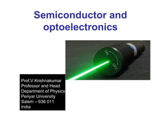
  • 1. Semiconductor and optoelectronics Prof.V.Krishnakumar Professor and Head Department of Physics Periyar University Salem – 636 011 India
  • 2. Electricity • Electricity is the flow of electrons • Good conductors (copper) have easily released electrons that drift within the metal • Under influence of electric field, electrons flow in a current –magnitude of current depends on magnitude of voltage applied to circuit, and the resistance in the path of the circuit • Current flow governed by Ohm’s Law + V = IR electron flow direction -
  • 3. Electron Bands • Electrons circle nucleus in defined shells – K 2 electrons – L 8 electrons – M 18 electrons – N 32 electrons • Within each shell, electrons are further grouped into subshells – s 2 electrons – p 6 electrons – d 10 electrons – f 14 electrons • electrons are assigned to shells and subshells from inside out – Si has 14 electrons: 2 K, 8 L, 4 M 10 6 2 M shell K L d p s
  • 4. Electronic Materials • The goal of electronic materials is to generate and control the flow of an electrical current. • Electronic materials include: 1. Conductors: have low resistance which allows electrical current flow 2. Insulators: have high resistance which suppresses electrical current flow 3. Semiconductors: can allow or suppress electrical current flow
  • 5. Conductors • Good conductors have low resistance so electrons flow through them with ease. • Best element conductors include: – Copper, silver, gold, aluminum, & nickel • Alloys are also good conductors: – Brass & steel • Good conductors can also be liquid: – Salt water
  • 6. Conductor Atomic Structure • The atomic structure of good conductors usually includes only one electron in their outer shell. – It is called a valence electron. – It is easily striped from the atom, producing current flow. Copper Atom
  • 7. Insulators • Insulators have a high resistance so current does not flow in them. • Good insulators include: – Glass, ceramic, plastics, & wood • Most insulators are compounds of several elements. • The atoms are tightly bound to one another so electrons are difficult to strip away for current flow.
  • 8. Semiconductors • Semiconductors are materials that essentially can be conditioned to act as good conductors, or good insulators, or any thing in between. • Common elements such as carbon, silicon, and germanium are semiconductors. • Silicon is the best and most widely used semiconductor.
  • 9. Semiconductor Valence Orbit • The main characteristic of a semiconductor element is that it has four electrons in its outer or valence orbit.
  • 10. Crystal Lattice Structure • The unique capability of semiconductor atoms is their ability to link together to form a physical structure called a crystal lattice. • The atoms link together with one another sharing their outer electrons. • These links are called covalent bonds. 2D Crystal Lattice Structure
  • 11. 3D Crystal Lattice Structure
  • 12. Semiconductors can be Insulators • If the material is pure semiconductor material like silicon, the crystal lattice structure forms an excellent insulator since all the atoms are bound to one another and are not free for current flow. • Good insulating semiconductor material is referred to as intrinsic. • Since the outer valence electrons of each atom are tightly bound together with one another, the electrons are difficult to dislodge for current flow. • Silicon in this form is a great insulator. • Semiconductor material is often used as an insulator.
  • 13. Doping • To make the semiconductor conduct electricity, other atoms called impurities must be added. • “Impurities” are different elements. • This process is called doping.
  • 14. Semiconductors can be Conductors • An impurity, or element like arsenic, has 5 valence electrons. • Adding arsenic (doping) will allow four of the arsenic valence electrons to bond with the neighboring silicon atoms. • The one electron left over for each arsenic atom becomes available to conduct current flow.
  • 15. N-Type Semiconductor The silicon doped with extra electrons is called an “N type” semiconductor. “N” is for negative, which is the charge of an electron.
  • 16. Resistance Effects of Doping • If you use lots of arsenic atoms for doping, there will be lots of extra electrons so the resistance of the material will be low and current will flow freely. • If you use only a few boron atoms, there will be fewer free electrons so the resistance will be high and less current will flow. • By controlling the doping amount, virtually any resistance can be achieved.
  • 17. Current Flow in N-type Semiconductors • The DC voltage source has a positive terminal that attracts the free electrons in the semiconductor and pulls them away from their atoms leaving the atoms charged positively. • Electrons from the negative terminal of the supply enter the semiconductor material and are attracted by the positive charge of the atoms missing one of their electrons. • Current (electrons) flows from the positive terminal to the negative terminal.
  • 18. Another Way to Dope • You can also dope a semiconductor material with an atom such as boron that has only 3 valence electrons. • The 3 electrons in the outer orbit do form covalent bonds with its neighboring semiconductor atoms as before. But one electron is missing from the bond. • This place where a fourth electron should be is referred to as a hole. • The hole assumes a positive charge so it can attract electrons from some other source. • Holes become a type of current carrier like the electron to support current flow.
  • 19. P-Type Semiconductor Silicon doped with material missing electrons that produce locations called holes is called “P type” semiconductor. “P” is for positive, which is the charge of a hole.
  • 20. Current Flow in P-type Semiconductors • Electrons from the negative supply terminal are attracted to the positive holes and fill them. • The positive terminal of the supply pulls the electrons from the holes leaving the holes to attract more electrons. • Current (electrons) flows from the negative terminal to the positive terminal. • Inside the semiconductor current flow is actually by the movement of the holes from positive to negative.
  • 21. Introduction to Semiconductor Devices Semiconductor p-n junction diodes p n
  • 22. p-n junction formation p-type material Semiconductor material doped with acceptors. Material has high hole concentration Concentration of free electrons in p-type material is very low. n-type material Semiconductor material doped with donors. Material has high concentration of free electrons. Concentration of holes in n-type material is very low.
  • 23. p-n junction formation p-type material Contains NEGATIVELY charged acceptors (immovable) and POSITIVELY charged holes (free). Total charge = 0 n-type material Contains POSITIVELY charged donors (immovable) and NEGATIVELY charged free electrons. Total charge = 0
  • 24. Diffusion A substance, the purple dots, in solution. A membrane prevents movement of the water and the molecules from crossing from one side of the beaker to the other. Now that the gates have been opened, the random movements of the molecules have caused, overtime, the number of molecules to be equal on the two sides of the barrier.
  • 25. Diffusion As a result of diffusion, the molecules or other free particles distribute uniformly over the entire volume
  • 26. p- n junction formation What happens if n- and p-type materials are in close contact? Being free particles, electrons start diffusing from n-type material into p-material Being free particles, holes, too, start diffusing from p-type material into n-material Have they been NEUTRAL particles, eventually all the free electrons and holes had uniformly distributed over the entire compound crystal. However, every electrons transfers a negative charge (-q) onto the p-side and also leaves an uncompensated (+q) charge of the donor on the n-side. Every hole creates one positive charge (q) on the n-side and (-q) on the p-side
  • 27. p- n junction formation What happens if n- and p-type materials are in close contact? p-type n-type Electrons and holes remain staying close to the p-n junction because negative and positive charges attract each other. Negative charge stops electrons from further diffusion Positive charge stops holes from further diffusion The diffusion forms a dipole charge layer at the p-n junction interface. There is a “built-in” VOLTAGE at the p-n junction interface that prevents penetration of electrons into the p-side and holes into the n-side.
  • 28. p- n junction current – voltage characteristics What happens when the voltage is applied to a p-n junction? p-type n-type The polarity shown, attracts holes to the left and electrons to the right. According to the current continuity law, the current can only flow if all the charged particles move forming a closed loop However, there are very few holes in n-type material and there are very few electrons in the p-type material. There are very few carriers available to support the current through the junction plane For the voltage polarity shown, the current is nearly zero
  • 29. p- n junction current – voltage characteristics What happens if voltage of opposite polarity is applied to a p-n junction? p-type n-type The polarity shown, attracts electrons to the left and holes to the right. There are plenty of electrons in the n-type material and plenty of holes in the p-type material. There are a lot of carriers available to cross the junction. When the voltage applied is lower than the built-in voltage, the current is still nearly zero When the voltage exceeds the built-in voltage, the current can flow through the p-n junction
  • 30. Diode current – voltage (I-V) characteristics Semiconductor diode consists of a p-n junction with two contacts attached to the p- and n- sides V 0 ù p n I I qV S exp = æ 1 úû é êë ö çè - ÷ø kT IS is usually a very small current, IS ≈ 10-17 …10-13 A When the voltage V is negative (“reverse” polarity) the exponential term ≈ -1; The diode current is ≈ IS ( very small). When the voltage V is positive (“forward” polarity) the exponential term increases rapidly with V and the current is high.
  • 31. p- n diode applications: Light emitters P-n junction can emit the light when forward biased p-type n-type +- Electrons drift into p-material and find plenty of holes there. They “RECOMBINE” by filling up the “empty” positions. Holes drift into n-material and find plenty of electrons there. They also “RECOMBINE” by filling up the “empty” positions. The energy released in the process of “annihilation” produces PHOTONS – the particles of light
  • 32. +- p- n diode applications: Photodetectors P-n junction can detect light when reverse biased p-type n-type When the light illuminates the p-n junction, the photons energy RELEASES free electrons and holes. They are referred to as PHOTO-ELECTRONS and PHOTO-HOLES The applied voltage separates the photo-carriers attracting electrons toward “plus” and holes toward “minus” As long as the light is ON, there is a current flowing through the p-n junction
  • 33. CB VB WWhheenn tthhee eelleeccttrroonn ffaallllss ddoowwnn ffrroomm ccoonndduuccttiioonn bbaanndd aanndd ffiillllss iinn aa hhoollee iinn vvaalleennccee bbaanndd,, tthheerree iiss aann oobbvviioouuss lloossss ooff eenneerrggyy..
  • 34. IInn oorrddeerr ttoo aacchhiieevvee aa rreeaassoonnaabbllee eeffffiicciieennccyy ffoorr pphhoottoonn eemmiissssiioonn,, tthhee sseemmiiccoonndduuccttoorr mmuusstt hhaavvee aa ddiirreecctt bbaanndd ggaapp.. CB VB
  • 35. FFoorr eexxaammppllee;; SSiilliiccoonn iiss kknnoowwnn aass aann iinnddiirreecctt bbaanndd--ggaapp mmaatteerriiaall.. aass aann eelleeccttrroonn ggooeess ffrroomm tthhee bboottttoomm ooff tthhee ccoonndduuccttiioonn bbaanndd ttoo tthhee ttoopp ooff tthhee vvaalleennccee bbaanndd;; iitt mmuusstt aallssoo uunnddeerrggoo aa ssiiggnniiffiiccaanntt cchhaannggee iinn mmoommeennttuumm.. CB VB WWhhaatt tthhiiss mmeeaannss iiss tthhaatt E k
  • 36. • As we all kknnooww,, wwhheenneevveerr ssoommeetthhiinngg cchhaannggeess ssttaattee,, oonnee mmuusstt ccoonnsseerrvvee nnoott oonnllyy eenneerrggyy,, bbuutt aallssoo mmoommeennttuumm.. • IInn tthhee ccaassee ooff aann eelleeccttrroonn ggooiinngg ffrroomm ccoonndduuccttiioonn bbaanndd ttoo tthhee vvaalleennccee bbaanndd iinn ssiilliiccoonn,, bbootthh ooff tthheessee tthhiinnggss ccaann oonnllyy bbee ccoonnsseerrvveedd:: The transition also creates a quantized set of lattice vibrations, called phonons, or "heat“ .
  • 37. • PPhhoonnoonnss ppoosssseessss bbootthh eenneerrggyy aanndd mmoommeennttuumm.. • TThheeiirr ccrreeaattiioonn uuppoonn tthhee rreeccoommbbiinnaattiioonn ooff aann eelleeccttrroonn aanndd hhoollee aalllloowwss ffoorr ccoommpplleettee ccoonnsseerrvvaattiioonn ooff bbootthh eenneerrggyy aanndd mmoommeennttuumm.. • AAllll ooff tthhee eenneerrggyy wwhhiicchh tthhee eelleeccttrroonn ggiivveess uupp iinn ggooiinngg ffrroomm tthhee ccoonndduuccttiioonn bbaanndd ttoo tthhee vvaalleennccee bbaanndd ((11..11 eeVV)) eennddss uupp iinn pphhoonnoonnss,, wwhhiicchh iiss aannootthheerr wwaayy ooff ssaayyiinngg tthhaatt tthhee eelleeccttrroonn hheeaattss uupp tthhee ccrryyssttaall..
  • 38. In aa ccllaassss ooff mmaatteerriiaallss ccaalllleedd ddiirreecctt bbaanndd--ggaapp sseemmiiccoonndduuccttoorrss;; »tthhee ttrraannssiittiioonn ffrroomm ccoonndduuccttiioonn bbaanndd ttoo vvaalleennccee bbaanndd iinnvvoollvveess eesssseennttiiaallllyy nnoo cchhaannggee iinn mmoommeennttuumm.. »PPhhoottoonnss,, iitt ttuurrnnss oouutt,, ppoosssseessss aa ffaaiirr aammoouunntt ooff eenneerrggyy (( sseevveerraall eeVV/pphhoottoonn iinn ssoommee ccaasseess )) bbuutt tthheeyy hhaavvee vveerryy lliittttllee mmoommeennttuumm aassssoocciiaatteedd wwiitthh tthheemm..
  • 39. • Thus, for a ddiirreecctt bbaanndd ggaapp mmaatteerriiaall,, tthhee eexxcceessss eenneerrggyy ooff tthhee eelleeccttrroonn--hhoollee rreeccoommbbiinnaattiioonn ccaann eeiitthheerr bbee ttaakkeenn aawwaayy aass hheeaatt,, oorr mmoorree lliikkeellyy,, aass aa pphhoottoonn ooff lliigghhtt.. • TThhiiss rraaddiiaattiivvee ttrraannssiittiioonn tthheenn ccoonnsseerrvveess eenneerrggyy aanndd mmoommeennttuumm bbyy ggiivviinngg ooffff lliigghhtt wwhheenneevveerr aann eelleeccttrroonn aanndd hhoollee rreeccoommbbiinnee.. CB VB TThhiiss ggiivveess rriissee ttoo ((ffoorr uuss)) aa nneeww ttyyppee ooff ddeevviiccee;; tthhee lliigghhtt eemmiittttiinngg ddiiooddee ((LLEEDD))..
  • 40. What is LED? Semiconductors bring quality to light! LED are semiconductor p-n junctions that under forward bias conditions can emit radiation by electroluminescence in the UV, visible or infrared regions of the electromagnetic spectrum. The qaunta of light energy released is approximately proportional to the band gap of the semiconductor.
  • 41. Getting to know LED Advantages of Light Emitting Diodes (LEDs) Longevity: The light emitting element in a diode is a small conductor chip rather than a filament which greatly extends the diode’s life in comparison to an incandescent bulb (10 000 hours life time compared to ~1000 hours for incandescence light bulb) Efficiency: Diodes emit almost no heat and run at very low amperes. Greater Light Intensity: Since each diode emits its own light Cost: Not too bad Robustness: Solid state component, not as fragile as incandescence light bulb
  • 42. LED chip is the part that we shall deal with in this course
  • 43. Luminescence is the process behind light emission • Luminescence is a term used to describe the emission of radiation from a solid when the solid is supplied with some form of energy. • Electroluminescence  excitation results from the application of an electric field • In a p-n junction diode injection electroluminescence occurs resulting in light emission when the junction is forward biased
  • 44. PPrroodduucciinngg pphhoottoonn EElleeccttrroonnss rreeccoommbbiinnee wwiitthh hhoolleess.. EEnneerrggyy ooff pphhoottoonn iiss tthhee eenneerrggyy ooff bbaanndd ggaapp.. CB VB e-h
  • 45. How does it work? P-n junction Electrical Contacts A typical LED needs aa pp--nn jjuunnccttiioonn There are a lot of electrons and holes at the junction due to excitations Electrons from n need to be injected to p to promote recombination Junction is biased to produce even more e-h and to inject electrons from n to p for recombination to happen Recombination produces light!!
  • 46. Injection Luminescence in LED  Under forward bias – majority carriers from both sides of the junction can cross the depletion region and entering the material at the other side.  Upon entering, the majority carriers become minority carriers  For example, electrons in n-type (majority carriers) enter the p-type to become minority carriers  The minority carriers will be larger  minority carrier injection  Minority carriers will diffuse and recombine with the majority carrier.  For example, the electrons as minority carriers in the p-region will recombine with the holes. Holes are the majority carrier in the p-region.  The recombination causes light to be emitted  Such process is termed radiative recombination.
  • 47. MMAATTEERRIIAALLSS FFOORR LLEEDDSS • TThhee sseemmiiccoonndduuccttoorr bbaannddggaapp eenneerrggyy ddeeffiinneess tthhee eenneerrggyy ooff tthhee eemmiitttteedd pphhoottoonnss iinn aa LLEEDD.. • TToo ffaabbrriiccaattee LLEEDDss tthhaatt ccaann eemmiitt pphhoottoonnss ffrroomm tthhee iinnffrraarreedd ttoo tthhee uullttrraavviioolleett ppaarrttss ooff tthhee ee..mm.. ssppeeccttrruumm,, tthheenn wwee mmuusstt ccoonnssiiddeerr sseevveerraall ddiiffffeerreenntt mmaatteerriiaall ssyysstteemmss.. • NNoo ssiinnggllee ssyysstteemm ccaann ssppaann tthhiiss eenneerrggyy bbaanndd aatt pprreesseenntt,, aalltthhoouugghh tthhee 33--55 nniittrriiddeess ccoommee cclloossee.. CB VB
  • 48. • Unfortunately, many ooff ppootteennttiiaallllllyy uusseeffuull 22--66 ggrroouupp ooff ddiirreecctt bbaanndd--ggaapp sseemmiiccoonndduuccttoorrss ((ZZnnSSee,,ZZnnTTee,,eettcc..)) ccoommee nnaattuurraallllyy ddooppeedd eeiitthheerr pp-- ttyyppee,, oorr nn--ttyyppee,, bbuutt tthheeyy ddoonn’’tt lliikkee ttoo bbee ttyyppee-- ccoonnvveerrtteedd bbyy oovveerrddooppiinngg.. • TThhee mmaatteerriiaall rreeaassoonnss bbeehhiinndd tthhiiss aarree ccoommpplliiccaatteedd aanndd nnoott eennttiirreellyy wweellll--kknnoowwnn.. • TThhee ssaammee pprroobblleemm iiss eennccoouunntteerreedd iinn tthhee 33--55 nniittrriiddeess aanndd tthheeiirr aallllooyyss IInnNN,, GGaaNN,, AAllNN,, IInnGGaaNN,, AAllGGaaNN,, aanndd IInnAAllGGaaNN.. TThhee aammaazziinngg tthhiinngg aabboouutt 33--55 nniittrriiddee aallllooyy ssyysstteemmss iiss tthhaatt aappppeeaarr ttoo bbee ddiirreecctt ggaapp tthhrroouugghhoouutt..
  • 49. Construction of Typical LED Light output n Substrate Al SiO2 Electrical contacts p
  • 50. LED Construction  Efficient light emitter is also an efficient absorbers of radiation therefore, a shallow p-n junction required.  Active materials (n and p) will be grown on a lattice matched substrate.  The p-n junction will be forward biased with contacts made by metallisation to the upper and lower surfaces.  Ought to leave the upper part ‘clear’ so photon can escape.  The silica provides passivation/device isolation and carrier confinement
  • 51. Efficient LED  Need a p-n junction (preferably the same semiconductor material only different dopants)  Recombination must occur  Radiative transmission to give out the ‘right coloured LED’  ‘Right coloured LED’  hc/l = Ec-Ev = Eg  so choose material with the right Eg  Direct band gap semiconductors to allow efficient recombination  All photons created must be able to leave the semiconductor  Little or no reabsorption of photons
  • 52. Correct band gap Direct band gap Materials Requirements Material can be made p and n-type Efficient radiative pathways must exist
  • 53. Direct band gap Candidate Materials materials e.g. GaAs not Si  UV-ED l ~0.5-400nm Eg > 3.25eV  LED - l ~450-650nm Eg = 3.1eV to 1.6eV  IR-ED- l ~750nm- 1nm Eg = 1.65eV Readily Materials with refractive doped n or p-types index that could allow light to ‘get out’
  • 54. Candidate Materials Group III-V & Group II-VI Group II Group III Group IV Group V iii iv v ii Al Ga In N P As Periodic Table to show group III-V and II-V binaries
  • 55. Candidate Materials Group III-V & Group II-VI Group II Group III Group IV Group V iii iv v ii Al Ga In N P As Periodic Table to show group III-V and II-V binaries
  • 56. CCoolloorr NNaammee WWaavveelleennggtthh ((NNaannoommeetteerrss)) SSeemmiiccoonndduuccttoorr CCoommppoossiittiioonn IInnffrraarreedd 888800 GGaaAAllAAss//GGaaAAss UUllttrraa RReedd 666600 GGaaAAllAAss//GGaaAAllAAss SSuuppeerr RReedd 663333 AAllGGaaIInnPP SSuuppeerr OOrraannggee 661122 AAllGGaaIInnPP OOrraannggee 660055 GGaaAAssPP//GGaaPP YYeellllooww 558855 GGaaAAssPP//GGaaPP IInnccaannddeesscceenntt WWhhiittee 44550000KK ((CCTT)) IInnGGaaNN//SSiiCC PPaallee WWhhiittee 66550000KK ((CCTT)) IInnGGaaNN//SSiiCC CCooooll WWhhiittee 88000000KK ((CCTT)) IInnGGaaNN//SSiiCC PPuurree GGrreeeenn 555555 GGaaPP//GGaaPP SSuuppeerr BBlluuee 447700 GGaaNN//SSiiCC BBlluuee VViioolleett 443300 GGaaNN//SSiiCC UUllttrraavviioolleett 339955 IInnGGaaNN//SSiiCC
  • 57. Getting to know LED Advantages of Light Emitting Diodes (LEDs) Longevity: The light emitting element in a diode is a small conductor chip rather than a filament which greatly extends the diode’s life in comparison to an incandescent bulb (10 000 hours life time compared to ~1000 hours for incandescence light bulb) Efficiency: Diodes emit almost no heat and run at very low amperes. Greater Light Intensity: Since each diode emits its own light Cost: Not too bad Robustness: Solid state component, not as fragile as incandescence light bulb
  • 58. LED chip is the part that we shall deal with in this course
  • 59. Some Types of LEDs Bargraph 7-segment Starburst Dot matrix
  • 61. Your fancy telephone, i-pod, palm pilot and digital camera
  • 63. • What is the word LASER stands for? • Light amplification by Stimulated Emission of Radiation
  • 64. Stimulated Emission E2 E1 hu (a) Absorption hu E2 E2 E1 E1 (b) Spontaneous emission hu In hu Out hu (c) Stimulated emission Absorption, spontaneous (random photon) emission and stimulated emission. © 1999 S.O. Kasap, Optoelectronics (Prentice Hall) In stimulated emission, an incoming photon with energy hu stimulates the emission process by inducing electrons in E2 to transit down to E1. While moving down to E1, photon of the same energy hu will be emitted Resulting in 2 photons coming out of the system Photons are amplified – one incoming photon resulting in two photons coming out.
  • 65. Population Inversion • Non equilibrium distribution of atoms among the various energy level atomic system • To induce more atoms in E2, i.e. to create population inversion, a large amount of energy is required to excite atoms to E2 • The excitation process of atoms so N2 > N2 is called pumping • It is difficult to attain pumping when using two-level-system. • Require 3-level system instead More atoms here E2 E1 N2> N1 N2 N1 E3 E2 E1 There level system
  • 66. Principles of Laser E 3 E 1 hu13 E 2 Metastable state E 3 E 1 E 2 hu32 E 3 E 1 E 2 E 3 E 1 E 2 OUT hu21 hu21 Coherent photons (a) (b) (c) (d) . IN • In actual case, excite atoms from E1 to E3. • Exciting atoms from E1 to E3 optical pumping • Atoms from E3 decays rapidly to E2 emitting hu3 • If E2 is a long lived state, atoms from E2 will not decay to E1 rapidly • Condition where there are a lot of atoms in E2 population inversion achieved! i.e. between E2 and E1.
  • 67. Coherent Photons Production (explanation of (d)) • When one atom in E2 decays spontaneously, a random photon resulted which will induce stimulated photon from the neighbouring atoms • The photons from the neighbouring atoms will stimulate their neighbours and form avalanche of photons. • Large collection of coherent photons resulted.
  • 68. Laser Diode Principle • Consider a p-n junction • In order to design a laser diode, the p-n junction must be heavily doped. • In other word, the p and n materials must be degenerately doped • By degenerated doping, the Fermi level of the n-side will lies in the conduction band whereas the Fermi level in the p-region will lie in the valance band.
  • 69. Diode Laser Operation p+ n+ E Fn E g (a) E c E v E v Holes inVB Junction Electrons inCB Electrons E c p+ E g V n+ (b) E Fn eV E Fp Inversion region E Fp E c E c eV o •P-n junction must be degenerately doped. •Fermi level in valance band (p) and conduction band (n). •No bias, built n potential; eVo barrier to stop electron and holes movement •Forward bias, eV> Eg •Built in potential diminished to zero •Electrons and holes can diffuse to the space charge layer
  • 70. Application of Forward Bias • Suppose that the degenerately doped p-n junction is forward biased by a voltage greater than the band gap; eV > Eg • The separation between EFn and EFp is now the applied potential energy • The applied voltage diminished the built-in potential barrier, eVo to almost zero. • Electrons can now flow to the p-side • Holes can now flow to the n-side
  • 71. Population Inversion in Diode Laser hu Optical gain EFn - EFp Eg 0 Optical absorption Energy EFn Ec Ev CB VB Electrons in CB Holes in VB = Empty states Density of states EFp eV At T > 0 At T = 0 (a) (b) (a) The density of states and energy distribution of electrons and holes in the conduction and valence bands respectively at T » 0 in the SCL under forward bias such that EFn - EFp > Eg. Holes in the VB are empty states. (b) Gain vs. photon energy. © 1999 S.O. Kasap, Optoelectronics (Prentice Hall)
  • 72. Population Inversion in Diode Laser Electrons in CB EFn EFp CB VB Eg Holes in VB eV EFn-EfP = eV eV > Eg eV = forward bias voltage Fwd Diode current pumping  injection pumping More electrons in the conduction band near EC Than electrons in the valance band near EV There is therefore a population inversion between energies near EC and near EV around the junction. This only achieved when degenerately doped p-n junction is forward bias with energy > Egap
  • 73. The Lasing Action • The population inversion region is a layer along the junction  also call inversion layer or active region • Now consider a photon with E = Eg • Obviously this photon can not excite electrons from EV since there is NO electrons there • However the photon CAN STIMULATE electron to fall down from CB to VB. • Therefore, the incoming photon stimulates emission than absorption • The active region is then said to have ‘optical gain’ since the incoming photon has the ability to cause emission rather than being absorbed.
  • 74. Pumping Mechanism in Laser Diode • It is obvious that the population inversion between energies near EC and those near EV occurs by injection of large charge carrier across the junction by forward biasing the junction. • Therefore the pumping mechanism is FORWARD DIODE CURRENT  Injection pumping
  • 75. For Successful Lasing Action: 1. Optical Gain (not absorb) Achieved by population inversion 2. Optical Feedback Achieved by device configuration Needed to increase the total optical amplification by making photons pass through the gain region multiple times Insert 2 mirrors at each end of laser This is term an oscillator cavity or Fabry Perot cavity Mirrors are partly transmitted and party reflected
  • 77. Optical Power in Laser is Very High due to Optical Feedback and Higher Forward Bias Current. Threshold current density
  • 78. Direct Gap Diode Laser • Direct band gap  high probability of electrons-holes recombination  radioactively • The recombination radiation may interact with the holes in the valance band and being absorbed or interact with the electrons in the conduction band thereby stimulating the production of further photons of the same frequency  stimulated emission
  • 81. InGaN and AlGaN • InGaN and AlGaN have been produced over the entire composition range between their component binaries; InN, GaN, AlN • InAlN is less explored. • GaN and AlN are fairly well lattice-matched to SiC substrates, • SiC has substrate is better as it can be doped (dopability) and high thermal conductivity relative to more commonly used Al2O3 substrates. • AlN and GaN can be used for high temperature application due to wide bandgaps and low intrinsic carrier concentrations.