International Journal of Engineering Research and Development (IJERD)

journal publishing, how to publish research paper, Call For research paper, international journal, publishing a paper, IJERD, journal of science and technology, how to get a research paper published, publishing a paper, publishing of journal, publishing of research paper, reserach and review articles, IJERD Journal, How to publish your research paper, publish research paper, open access engineering journal, Engineering journal, Mathemetics journal, Physics journal, Chemistry journal, Computer Engineering, Computer Science journal, how to submit your paper, peer reviw journal, indexed journal, reserach and review articles, engineering journal, www.ijerd.com, research journals, yahoo journals, bing journals, International Journal of Engineering Research and Development, google journals, hard copy of journal
![Low Power, Area And Delay Efficient Carry Select Adder Using...
2
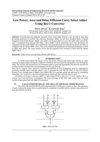
Fig 2: 4 bit BEC evaluation of XOR gate
Contributed by that gate. The delay and area evaluation methodology considers all gates to be made up
of AND, OR, and INVERTER, each having delay equal to 1 unit and area equal to 1 unit. We then add up the
number of gates in the longest path of a logic block that contributes to the maximum delay. The area evaluation
is done by counting the total number of AOI gates required for each logic block. Based on this approach, the
CSLA adder blocks of 2:1 mux, Half Adder (HA), and FA are evaluated and listed in Table I.
III. BINARY TO EXCESS-1 CONVERTER
To reduce the area and power consumption Binary Excess-1 converter instead of RCA with Cin = 1.
This is the main concept of the paper,so as to reduce dealy compared to regular SQRT CSLA. To replace the n-
bit RCA, an n+1 bit BEC is required. A structured and the function table of a 4-b BEC are shown in fig 2 and
table II, respectively.
Fig3 illustrates how the basic function of the CSLA is obtained by using the 4-bit BEC together with
the mux. One input of the 8:4 mux gets as it input (B3,B2,B1,and B0) and another input of the mux is the BEC
output. This produces the two possible partial results in parallel and the mux is used to select either the BEC
output or the direct inputs according to the control signal cin. The Boolean expressions of the 4-bit BEC is listed
as
X0 = ~B0
X1 = B0 ^ B1
X2 = B2 ^ (B0 & B1)
X3 = B3 ^ (B0 & B1 & B2)
Table1 delay and area count of the basic blocks of CSLA
IV. DELAY AND AREA EVALUATION METHODOLOGY OF REGULAR 16-B SQRT
CSLA
The structure of the 16-b regular SQRT CSLA is shown in fig 4. It has five groups of different size
RCA. The delay and area evaluation of each group are shown in fig 6, in which the numerical specify the delay
values, e.g., sum2 requires 10 gate delays. The steps leading to the evaluation are as follows.
1) The group2 [in fig 6(a)] has two sets of 2- b RCA ,based on the consideration of delay values of table I.
the arrival time of selection input c1 [time(t) = 7] of 6:3 mux is earlier than s3[t = 8] and later than s2[t = 6].
Thus, sum3[t = 11] is summation S3 and mux[t = 3] and sum2[t = 10] is summation of c1 and mux.
2) Other than group2, the arrival time of mux selection input is always greater than the RCA’s. thus the
delay of group3 to group5 is determined , respectively as follows: arrival time of data outputs from the
{c6, sum[6 : 4]} = c3[t = 10] + mux
{c10, sum[10:7]} = c6[t= 13] + mux](data:image/gif;base64,R0lGODlhAQABAIAAAAAAAP///yH5BAEAAAAALAAAAAABAAEAAAIBRAA7)
Recomendados
Recomendados
Mais conteúdo relacionado
Mais procurados
Mais procurados (20)
Destaque
Destaque (20)
Semelhante a International Journal of Engineering Research and Development (IJERD)
Semelhante a International Journal of Engineering Research and Development (IJERD) (20)
Mais de IJERD Editor
Mais de IJERD Editor (20)
Último
Último (20)
International Journal of Engineering Research and Development (IJERD)
- 1. International Journal of Engineering Research and Development e-ISSN: 2278-067X, p-ISSN: 2278-800X, www.ijerd.com Volume 8, Issue 2 (August 2013), PP. 01-07 1 Low Power, Area and Delay Efficient Carry Select Adder Using Bec-1 Converter Shaik Jabeen1 , K.Upendra Raju2 1 Post graduate student, Dept of ECE, KLMCEW, Kadapa, A.P. 2 Associate Professor, Dept of ECE, KLMCEW, Kadapa, A.P Abstract:- In performing fast arithmetic functions, Carry select adder (CSLA) is one of used in many data processing processors to perform fast arithmetic functions. Adders are the basic building blocks in digital integrated circuit based designs. Ripple carry adders are slowest adders as every full adder must wait till the carry is generated from previous full adder. CSLA (SQRT CSLA) architecture have been developed and compared with the regular SQRT CSLA architecture. The proposed design has reduced area, power and delay as compared with the regular SQRT CSLA. This work evaluates the performance of the proposed designs in terms of delay, area, power. The result analysis shows that the proposed CSLA structure is better than the regular SQRT CSLA. Keywords:- ASIC, Power, area and delay efficient, BEC,CSLA. I. INTRODUCTION In VLSI system design the design of area and power efficient high speed logic systems are most essential. In digital adders, the speed of addition is limited by the time required to propagate a carry through the adder. The sum for each bit position in an elementary adder is generated sequentially only after the previous bit position has been summed and a carry propagated into the next position. The CSLA is used in many systems to overcome the problem of carry propagation delay by independently generating multiple carries and then select a carry to generate the sum. But the CSLA is not area efficient because it uses multiple pairs of Ripple Carry Adders (RCA) to generate partial sum and carry by considering carry input cin = 0 and cin=1, then the multiplexers are used to get final sum and carry are used. The Binary to Excess-1 converter (BEC) is used instead of RCA with Cin = 1 in the regular CSLA to achieve lower area and power consumption. The main advantage of this BEC logic comes from the lesser number of logic gates than Full Adder (FA) structure. II. CALCUATION OF DELAY AND AREA OF THE BASIC ADDER BLOCKS The AND, OR and INVERTER (AOI) implementation of XOR gate is shown in fig.1. The operations of gates between the dotted lines are performing the operations in parallel and the numeric representation of each gate indicates the delay. Fig1 : delay and area
- 2. Low Power, Area And Delay Efficient Carry Select Adder Using... 2 Fig 2: 4 bit BEC evaluation of XOR gate Contributed by that gate. The delay and area evaluation methodology considers all gates to be made up of AND, OR, and INVERTER, each having delay equal to 1 unit and area equal to 1 unit. We then add up the number of gates in the longest path of a logic block that contributes to the maximum delay. The area evaluation is done by counting the total number of AOI gates required for each logic block. Based on this approach, the CSLA adder blocks of 2:1 mux, Half Adder (HA), and FA are evaluated and listed in Table I. III. BINARY TO EXCESS-1 CONVERTER To reduce the area and power consumption Binary Excess-1 converter instead of RCA with Cin = 1. This is the main concept of the paper,so as to reduce dealy compared to regular SQRT CSLA. To replace the n- bit RCA, an n+1 bit BEC is required. A structured and the function table of a 4-b BEC are shown in fig 2 and table II, respectively. Fig3 illustrates how the basic function of the CSLA is obtained by using the 4-bit BEC together with the mux. One input of the 8:4 mux gets as it input (B3,B2,B1,and B0) and another input of the mux is the BEC output. This produces the two possible partial results in parallel and the mux is used to select either the BEC output or the direct inputs according to the control signal cin. The Boolean expressions of the 4-bit BEC is listed as X0 = ~B0 X1 = B0 ^ B1 X2 = B2 ^ (B0 & B1) X3 = B3 ^ (B0 & B1 & B2) Table1 delay and area count of the basic blocks of CSLA IV. DELAY AND AREA EVALUATION METHODOLOGY OF REGULAR 16-B SQRT CSLA The structure of the 16-b regular SQRT CSLA is shown in fig 4. It has five groups of different size RCA. The delay and area evaluation of each group are shown in fig 6, in which the numerical specify the delay values, e.g., sum2 requires 10 gate delays. The steps leading to the evaluation are as follows. 1) The group2 [in fig 6(a)] has two sets of 2- b RCA ,based on the consideration of delay values of table I. the arrival time of selection input c1 [time(t) = 7] of 6:3 mux is earlier than s3[t = 8] and later than s2[t = 6]. Thus, sum3[t = 11] is summation S3 and mux[t = 3] and sum2[t = 10] is summation of c1 and mux. 2) Other than group2, the arrival time of mux selection input is always greater than the RCA’s. thus the delay of group3 to group5 is determined , respectively as follows: arrival time of data outputs from the {c6, sum[6 : 4]} = c3[t = 10] + mux {c10, sum[10:7]} = c6[t= 13] + mux
- 3. Low Power, Area And Delay Efficient Carry Select Adder Using... 3 {cout,sum[15:11]} = c10[t =16] + mux 3) The one set of 2-b RCA in group2 has 2 FA for Cin and the other set has 1 FA and 1HA for Cin = 0.Based on the area count of table I, total number of gate counts in group2 of table I,the total number of gate counts in group2 is determined as follows: Gate count = 57 (FA + HA + MUX) FA = 39(3*13) HA = 6(1*6) Mux = 12(3*4) Fig.3: 4 bit BEC with 8:4 mux Table 2 function table of 4 b BEC Similarly, the estimated maximum delay and area of the other groups in the regular SQRT CSLA are evaluated and listed in table3. Fig 4: REGULAR 16 bit SQRT CSLA Fig 5: PROPOSED 16 bit SQRT CSLA
- 4. Low Power, Area And Delay Efficient Carry Select Adder Using... 4 Table 3 Delay and Area count of REGULAR SQRT CSLA Groups Groups Delay Area Group1 7 26 Group2 11 57 Group3 13 87 Group4 16 117 Group5 19 147 Table 4 Delay and Area count of PROPOSED SQRT CSLA Groups Groups Delay Area Group1 7 26 Group2 13 43 Group3 16 61 Group4 19 84 Group5 22 107 V. METHOD PROPOSED FOR 16 BIT CSLA BASED ON THE BEC-1 CONVERTER The structure of the proposed 16-b SQRT CSLA using BEC for RCA with Cin = 1 to optimize the area and power is shown in fig 5. We again split the structures into five groups. Tdelay and area evaluation of each group are shown in fig 7. 1) The group2 [in fig 7(a) has one 2-b RCA which has 1FA and 1HA for cin = 0. Instead of another 2-b RCA with cin = 1 a 3-b BEC is used which adds one to the output from 2-b RCA. Based on the consideration of delay values of table I,the arrival time of selection input c1[time(t) = 7] of 6:3 mux is earlier than the s3[t = 9] and c3[t = 10] and later than the s2[t = 4]. Thus, the sum3 and final c3[t = 10] and later than the s2[t = 4]. Thus, the sum3 and final c3(output from mux)are depending on s3 and mux and partial c3(input to mux) and mux ,respectively. The sum2 depends on c1 and mux. FA = 13(1 * 13) inputs from the BEC’s. thus , the delay of the remaining groups depends on the arrival time of mux selection input and the mux delay. For the remaining groups the arrival time of mux selection input is always greater than the arrival time of data 2) The area count of group2 is determined as follows: Gate cont = 43(FA+ HA + Mux + BEC) FA = 13(1 * 13) HA = 6(1 * 6) AND = 1 XOR = 10(2 * 5) Mux = 12(3*4) NOT = 1 3) Similarly, the estimated maximum delay and area of the other groups of the PROPOSED SQRT CSLA are evaluated and listed in table 4. Comparing tables 3 and 4, it is clear that the proposed system is better in delay and area,simulataneously in power.
- 5. Low Power, Area And Delay Efficient Carry Select Adder Using... 5 Fig 6 Delay and area evaluation of REGULAR SQRT CSLA: (a)group2, (b)group3, (c)group4 and (d)group5
- 6. Low Power, Area And Delay Efficient Carry Select Adder Using... 6 Fig 7 Delay and area evaluation of PROPOSED SQRT CSLA REGULAR and PROPOSED SQRT CSLA in (a)group 2, (b)group3, (c)group4, (d)group5 Fig 8 : Graphical charts representing area Table 3 Comparison of REGULAR and PROPOSED SQRT CSLA VII SIMULATION RESULTS Fig 9 simulation result for REGULAR 16 b SQRT CSLA
- 7. Low Power, Area And Delay Efficient Carry Select Adder Using... 7 VIII. CONCLUSION When the comparison between the SQRT CSLA and modified SQRT CSLA is considered, there is the difference in simple approach is proposed in this paper to reduce the area,delay and power of SQRT CSLA architecture. The reduced number of gates of this work offers the great advantage in the reduction of area, delay and also the total power. The compared results show that the proposed SQRT CSLA has delay, area and power are significantly reduced. Area and delay values of REGULAR SQRT CSLA and PROPOSED SQRT CSLA are given below, which are evaluated based on the Xilinx program of REGULAR SQRT and PROPOSED SQRT CSLA. 1) Area of REGULAR SQRT CSLA Number of Slices : 25 out of 4656 2% Number of 4 input LUTs : 45 out of 9312 2% Number of IOs : 50 Number of bonded IOBs : 50 out of 232 21% Delay of SQRT CSLA is 20.215ns Fig 10 simulation result for PROPOSED 16 b SQRT CSLA 2) Area of PROPOSED SQRT CSLA Number of Slices : 23 out of 4656 2% Number of 4 input LUTs : 40 out of 9312 2% Number of IOs : 50 Number of bonded IOBs :50 out of 232 21% Delay of MODIFIED SQRT CSLA is 18.867ns ACKNOWLEDGEMENT My wishes to acknowledge Sri K.Upendra Raju sir, Associate professor who guided me for the journal preparation. Thank you sir. REFERENCES [1] K. Rawwat, T. Darwish, and M. Bayoumi, “A low power carry select adder with reduces area”, proc. Of Midwest symposium on circuits and systems,pp. 218-221,2001. [2] W.Jeong and K.Roy, “robust high- performance low power adder”,proc,of the Asia and South Pacific Design Automatin Conference,pp.503-506,2003 [3] D.C Chen, L. M. Guerra,E. H. Ng, M. Potkonjak, D.P. Schultz and J. M. Rabaey, “An integrated system for rapid prototyping of high performance algorithm specific data paths,” in Proc. Application specific Array Processors, pp.134-148,Aug 1992. [4] T.Y. Chang and M. J. Hsiao, “ Carry Slecet adder using ripple carry adder,” Electronics letters, vol.34, no.22, pp.2101-2103,oct.1998 [5] B. Ramkumar, H. M. Kittur,and P. M. Khannan, “ASIC implantation of modified faster Carry sav adder,” Eur. J. Sci.Res.,Vol.42,no.1,pp 53-58,2010. [6] Y.Kim“64-bit carry select adder with reduced area,” Electron. Lett.,vol.37, no.10 ,pp.614-615.may 2001. [7] Milos D. Ercegovac and Thomas Lang, “Digital arthimetic,” Morgan Kaufmann, Elsevier INC,2004. [8] J. O. Bedrij, “ Carry Select Adder,” IRE Trans. Electronic Computrs,vol.11,pp.340-346,1962. [9] R. Hashmain, “A new design for high speed and high density carry select adders.’ Prceedings of IEEE Midwest Symp. On Circiuts and Systems.pp.1300-1303,2000.