An end-to-end design of a built-in self-test (BIST) infrastructure for 3D-stacked ICs that facilitate the use of BIST at multiple stages of 3D integration. The proposed BIST design is distributed, reusable, and reconfigurable, hence it is attractive for both pre-bond and post-bond testing. We also provide support for translating a static BIST schedule into a set of BIST control instructions. The BIST design is validated using detailed simulations of the various operating modes. It results on synthetic stacks assess the impact of inserting BIST in these designs in terms of area, timing, and power overhead. Results show that the overhead due to BIST is negligible. It also formulate a test-scheduling problem that aims at minimizing test time under BIST-resource and power constraints, and use two algorithms based on bin packing for solving the problem.
An Efficient Ic On chip Test Framework To Embed Tsv Testing In Memory Bist Using Dynamic Technique
1. Integrated Intelligent Research (IIR) International Journal of Business Intelligents
Volume: 05 Issue: 01 June 2016 Page No.16-20
ISSN: 2278-2400
16
An Efficient Ic On chip Test Framework To Embed Tsv
Testing In Memory Bist Using Dynamic Technique
G.Vithya1
, P. Krishnakumar2
1
Student, ME-VLSI Design, ,Sri Ramanujar Engineering,College, Vandalur, Kolappakkam,Chennai
2
Assistant Professor (OG), ,Dept of ECE, Sri Ramanujar Engineering College,Vandalur,Kolappakkam, Chennai
Email:vithyabeece16@gmail.com,krisskkr@gmail.com
Abstract—An end-to-end design of a built-in self-test (BIST)
infrastructure for 3D-stacked ICs that facilitate the use of BIST at
multiple stages of 3D integration. The proposed BIST design is
distributed, reusable, and reconfigurable, hence it is attractive for
both pre-bond and post-bond testing. We also provide support for
translating a static BIST schedule into a set of BIST control
instructions. The BIST design is validated using detailed
simulations of the various operating modes. It results on synthetic
stacks assess the impact of inserting BIST in these designs in
terms of area, timing, and power overhead. Results show that the
overhead due to BIST is negligible. It also formulate a test-
scheduling problem that aims at minimizing test time under
BIST-resource and power constraints, and use two algorithms
based on bin packing for solving the problem.
Keywords—BIST, 3DStacked IC, multiple stages.
I. INTRODUCTION
The emergence of three-dimensional (3D) stacking enables the
integration of multiple silicon dies in a vertical stack using
through-silicon visa (TSVs). In contrast to traditional core
integration technologies, 3D stacking overcomes the scalability
problems associated with large-scale integration of embedded
cores by offering benefits such as reduced wire length,
reduction in interconnect delays and power consumption, and
higher interconnect bandwidth. 3D-stacked memory chips are
on the verge of mainstream adoption and the semiconductor
industry is expected to further exploit the benefits of
3Dintegration in a variety of products, such as 3D NOC,
3Dmemory-on-processor, and 3D FPGA. The emergence of 3D
logic-logic stacks has also been predicted.Test schedules
created for pre-bond testing of individual dies may not be
applicable during post-bond testing because multiple dies can
be tested concurrently and the use of the same schedule can
lead to the violation of power constraints. Since a single BIST
resource can be shared by multiple cores, resource contention
should also be considered during the creation of test schedules.
For example, a memory BIST(MBIST) or a built-in self-repair
(BISR) block can be used for testing or self-repairing multiple
memory cores .Moreover, a BIST resource can be used for
testing a core located on a different die, e.g., memory vendors
may not choose to add MBIST logic on memory dies with
regular structures. Although there is published work on BIST
methods that support scheduling, there is no work known to us
that integrates scheduling with a BIST framework in the context
of 3D ICs.
The key contributions are as follows.
1. A unified framework for end-to-end BIST-based testing of
embedded cores, dies, and interconnects is proposed.
2. BIST framework is distributed, reusable, and reconfigurable.
The BIST controllers used in the pre-bond testing stage can also
be used during later stages of testing.
3. The controllers can be easily programmed to selectively
apply tests when required.
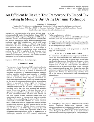
II. ARCHITECTURE OF THE SYSTEM
The architecture is based on a modular approach, in which the
various dies, their embedded IP cores, TSV-based interconnect,
and external I/O can be tested as separate units, before and/or
after bonding. Furthermore, the architecture leverages existing
2D DFT already present in the design, and adds a die-level
wrapper based on IEEE Std 1500 augmented with additional
features in order to be able to deals with 3D-SIC challenges
(e.g., to transport signals up and down through the stack). The
architecture is implemented and the simulation results show that
it provides the flexibiliy and the modularity is realized at the
cost of less than 0.1% area overhead when considering large
industrial chips.
Fig.1.Overview Of BIST Architecture
The building blocks of the proposed BIST framework consist of
die-level controllers, resource-level controllers, buffer
management modules, a completed-test broadcast bus (CTBS),
and CTBS arbiters (see Figure 1). BIST control instructions are
loaded through the bottom-most die. A die-level controller
controls every instruction going through the corresponding die.
2. Integrated Intelligent Research (IIR) International Journal of Business Intelligents
Volume: 05 Issue: 01 June 2016 Page No.16-20
ISSN: 2278-2400
17
It either dispatches an instruction to the appropriate resource
level controller or forwards it to the upper die if the
instruction is to be executed on a different die. Instructions
may not be executed as soon as they reach their target dies
due to resource or power constraints. A buffer management
module is thus used at every die for storing BIST instructions
until they become ready for execution. After a BIST
instruction is completed, all instructions that are waiting for
its completion are notified via the broadcast bus; access to
this bus is controlled by the arbiter located on every die. The
resource level controller configures the resources and invokes
each BIST run. The resource selector matches cores to
resource level controllers based on the test schedule. Next we
describe each component in detail.
III. BIST FRAMEWORK
The proposed BIST infrastructure is distributed, reusable, and
reconfigurable, and it provides support for end-to-end testing of
3D-stacked ICs. We assume BIST-ready cores with core-
specific BIST controllers connected to cores. We refer to core-
specific controllers as a resource in addition to any other BIST
infrastructure that the core-level controllers may use, e.g.,
LFSR/MISR pair. For instance, a BIST controller for pre-bond
or post-bond testing of TSVs is also categorized as resource in
this work. A single resource may be used for multiple tests, one
at a time.
A. BIST INSTRUCTION FORMAT
The dies communicate with each other using BIST instructions
that are encoded using the format shown in Fig. 2. The most
significant bit is the valid instruction bit, which if 1, indicates
that the instruction is valid; otherwise it is invalid. An
instruction is always valid when it is loaded, and it becomes
invalid later during its lifetime, as described in Section III.B.
The next bit indicates whether the instruction is in READY or
WAIT state. An instruction that is waiting for another
instruction to finish is categorized as a WAIT instruction,
otherwise it is a READY instruction—ready to be executed. An
instruction can be issued in both READY and WAIT mode. A
WAIT instruction is converted to a READY instruction through
a broadcast message.
Fig. 2.Bist Control Instrction Format
B. INSTRUCTION MANAGEMENT
Every BIST control instruction is fed through the bottommost
die. During testing, multiple cores can be tested simultaneously,
which implies that multiple instructions have to be placed
successively. Some of these instructions may not be processed
immediately because of temporary unavailability of a BIST
resource or due to power constraints. Such instructions have to
be stored temporarily in the stack. In order to alleviate this
problem, we propose a buffer-management module per die that
consists of buffers for storing the incoming and outgoing
instructions, and the related buffer controller.
Fig. 3.(a)Instruction Bmm;(B) Instruction With Multiple Slots.
As shown in Fig. 3(a), the buffer management module of a die
consists of an input buffer and an output buffer. All incoming
BIST instructions are stored in the input buffer and those
instructions that the die-level controller cannot absorb (because
the instructions are meant for a different die) are migrated to the
output buffer. An instruction in the output buffer of Die n is
transferred to the input buffer of Die n+1, only if the buffer
management module of Die n+1 is in a state to accept
instructions, i.e., if the input buffer of Die n+1 has free slots;
otherwise the instruction has to be temporarily stored in Die n.
As shown in Fig. 3(b), there can be multiple slots in a buffer.
Each slot is occupied by an instruction. Whether a slot is
occupied by an instruction is determined by the valid bit of the
instruction. Every buffer has a free-slot pointer that points to the
slot where the next instruction has to be filled. Therefore, the
free-slot pointer always points to a slot containing an invalid
instruction.
C. ARBITER
The buffer management module of each die keeps polling the
CTBS and changes the status of every instruction waiting for
the completed instruction to the READY state. A CTBS arbiter
grants permission to use the CTBS upon receiving a CLAIM
request from a resource-level controller.
Fig. 4.Arbiter Die And Their Interconnections.
The arbiter relinquishes the control of CTBS only when it is not
being used by any other controller. We have adopted a first-
come first-serve approach for arbitrating among the claim
requests from different controllers, and the arbiter may
prioritize among multiple resource-level controllers that assert
their respective CLAIM signals simultaneously. The arbiter
relinquishes the control of the bus through GRANT lines, after
3. Integrated Intelligent Research (IIR) International Journal of Business Intelligents
Volume: 05 Issue: 01 June 2016 Page No.16-20
ISSN: 2278-2400
18
which the IID of the completed instruction is put on the CTBS
by the corresponding controller. An arbiter communicates
with the arbiters present on adjacent dies for propagating the
IID through the stack. The interconnections between arbiters
in adjacent dies, highlighting the control signals that are used
for communication. Since the IID has to be propagated across
all dies, when an arbiter receives a CLAIM request from a
resource-level controller, it sends claim requests to the
arbitersof the adjacent dies through the CLAIM Aout port to
the die above it and through the CLAIM Bout port to the die
below it.
D. DIE-LEVEL CONTROLLER
Each die has a die-level controller that interacts with the
buffer management module of the same die to retrieve those
instructions that are in the READY state. If the DID field is
zero, the controller dispatches it to the resource-level
controller identified by the field RID. The controller also
interacts with die-level controllers of adjacent dies for
synchronized error propagation. The response collected after
running BIST on every die is sent back to the ATE for
debugging. In this work, we only use a pass/fail bit per core to
indicate whether the core has passed the test. On every die,
there is an error register that stores these pass/fail bits. As
shown in Fig. 5(a), the error registers on multiple die are
cascaded to form a single large shift register when the
response has to be collected, and the error bits are shifted out
in a serial fashion. The response is collected only when each
die has finished executing all instructions assigned to it. The
die-level controllers interact with each other for
synchronizing the shifting of cascaded error registers.
Fig. 5.(a) Cascaded Error Registers;
(b) Interconnections Between Dlc.
Fig. 5(b) shows the three input ports and the three output ports
of the controller that are used for communicating with die-level
controllers in adjacent dies. The three input ports and their
connectivity to the corresponding output ports are as follows:
1. s TFA in indicates that all tests in dies above the current die
are finished. It is connected to the output port s TFA out of the
upper die.
2. s SftErr in port receives a request sent from the die level
controller of the lower die, which enables the controller to start
shifting the error register. This port is connected to the signal s
SftErr out of the lower die.
3. s SftDone in port receives a signal indicating that every bit of
the error registers from all dies above the current die have been
shifted out. This port is connected to the s SftDone out port of the
upper die.
E. RESOURCE-LEVEL CONTROLLER
A resource-level controller is dedicated to a BIST resource and is
responsible for initializing and managing the resource. It is
present on the same die as the corresponding resource, but the
resource can be used for testing cores located in a different die.
Fig.6 describes a typical resource level controller. Initially, the
controller is in IDLE state, and moves to the RUNBIST state after
receiving the signal s init. In this state, the resource takes control,
and the resource level controller simply waits for the resource to
complete the BIST.
Fig. 6.STATE MACHINE FOR RLC
The resource (core-level controller if the BIST is testing a core)
first sets up the path to the intended core, initializes the
LFSR/MISR, and finally runs BIST. After BIST is completed,
the resource-level controller gets a completion
acknowledgement cmpl ack from the resource, and it moves to
the BDCAST state where the IID of the completed instruction is
broadcast on the CTBS. The FSM makes a transition to the
IDLE state if the arbiter on the same die is idle, identified by the
signal arb idle.
F. THROUGH SILICON VIAS
Another trend in microelectronics industry is to move dies ever
closer to each other. The communication between these stacked
dies is performed through wire bonds. The older PCB and MCP
style layout are still widely used today. However, in areas
where space is at a premium while the functionality
requirements are high like in the mobile market, SiP technology
is commonplace. From these sectors there is still a push to
package the chips tighter than ever before. This has been one of
the motivators of the Three-Dimensional Stacked IC (3DSIC) as
has been . 3D-SIC is similar to the SiP in concept, but instead of
using external wire bonds, the interconnect is made through the
dies themselves.
The microelectronics industry is researching the use of Through
Silicon Vias (TSVs), as a method for enabling the interconnect
between these stacked dies forming tiers in the 3D-SIC. TSVs
connect metal layers together just as ordinary vias do, but in this
case, the metal layers belong to two different tiers within the
stacked IC. TSVs are inter-tier vias, as they stick out
perpendicular to the metal layers right through the substrate of
their tier, enabling a connection to the metal layers of another
4. Integrated Intelligent Research (IIR) International Journal of Business Intelligents
Volume: 05 Issue: 01 June 2016 Page No.16-20
ISSN: 2278-2400
19
tier. The large benefit TSVs have in comparison to wire bonds
is their size. Wire bonds are considered expensive, slow and
energy-inefficient as interconnects due to their bulk. In
contrast, TSVs are much smaller and are comparable to on-
die interconnects. The downside is the costs for the additional
production steps necessary to create the TSVs.
Fig.7. Basic TSV
IV. SIMULATION TOOL
A. MODELSIM
Modelsim software is a HDL simulator manufactured by
mentor Graphics Corporation and can run independently
without ISE. Modelsim started version 6.0d. It is divided into
three sub windows:
1. Transcript Window (Bottom Window)
2. Workspace Window
3. Multiple Document interface (MDI) Window
The Workspace window displays information on the current
process. The bottom tab is used to select the desired process
page, which can be Project, Library, Sim and so on. The
transcript window keeps track of command history and
messages. It can also be used as a command -line interface to
enter ModelSim commands. The MDI window is an area to
display HDL text, wave form and so on.The bottom tab selects
the desired pages. Each sub window may be resized, docked or
undocked. Additional windows may appear for some
operations. The default layout can be restored by selecting
window.
Fig. 8.SIMULATION FLOW
Modelsim is a powerful simulator that can be used to simulate
the behaviour and performance of logic circuits. This tutorial
gives a rudimentary introduction to functional simulation of
circuits, using the graphical waveform editing capability of
Modelsim. The simulator allows the user to apply inputs to the
designed circuit, usually referred to as test vectors, and to observe
the outputs generated in response. The user can use the
Waveform Editor to represent the input signals as waveforms.
Functional simulation, which is used to verify the functional
correctness of a synthesized circuit.
B. VERILOG TOOLS
Verilog HDL descriptions of hardware design and test benches
are portable between design tools, and portable between design
centers and project partners. It safely invest in Verilog HDL
modelling effort and training, knowing that it will not be tied in to
a single tool vendor, but will be free to preserve your investment
across tools and platforms. Also, the design automation tool
vendors are themselves making a large investment in Verilog
HDL, ensuring a continuing supply of state-of-the-art Verilog
HDL Tools. Mixed-level simulation also verifies that the
interface of each block conforms to the plan; thereby eliminating
one of the most common causes for re-spins in complex mixed-
signal integrated circuits. Use of a top-down design methodology
based on mixed-level simulation results in a design process that
smoothly transitions from initial concept to final implementation,
with each step being verified with simulation. Thus, it eliminates
the discontinuities that are inherent to a bottom-up or primitive
top-down design style, greatly reducing the need for re-spins.
Such a design methodology also improves communication
between team members and increases the opportunity for parallel
development, which allows for a more dispersed design team and
offers a reduced time-to-market.
V. SIMULATION RESUTS
5. Integrated Intelligent Research (IIR) International Journal of Business Intelligents
Volume: 05 Issue: 01 June 2016 Page No.16-20
ISSN: 2278-2400
20
VI. CONCLUSION
An end-to-end framework for enabling selective BIST-based
testing at multiple test insertions during the integration of 3D-
stacked ICs had been presented. The proposed framework is
distributed, reusable and reconfigurable. The components of
this framework interact with each other through handshaking
protocols. The same test structures are used for pre-bond and
post-bond tests, and the controllers can be easily programmed
to apply tests selectively at deferent test insertions. Static
schedules created under resource and power constraints can
be encoded using a set of BIST control instructions that are
loaded in the stack for running BIST without external
intervention. A BIST test-scheduling problem under power
and resource constraints for 3D-stacked ICs and described
two solutions based on rectangle bin-packing algorithms. The
BIST design has been validated through detailed simulations,
and results on benchmark circuits show that the proposed
BIST framework has negligible impact on area, timing, and
power consumption.
Reference
[1] Mukesh Agrawal and Krishnendu Chakrabarty, ―A Distributed,
Reconfigurable, and Reusable BIST Infrastructure for 3D-Stacked ICs,
IEEE International Test Conference NC 27708, CA 95134.
[2] K. Banerjee et al., ―3-D ICs: A Novel Chip Design for Improving
Deep-Submicrometer Interconnect Performance and Systems-on-Chip
Integration,‖ Proc. IEEE, vol. 89, no. 5, pp. 602–633, May 2001.
[3] B. Feero and P. Pande, ―Networks-on-Chip in a Three-Dimensional
Environment: A Performance Evaluation,‖ IEEE Trans. Computers,
vol. 58, no. 1, pp. 32–45, Jan. 2009.
[4] G. H. Loh, Y. Xie, and B. Black, ―Processor Design in 3D Die-
Stacking Technologies,‖ IEEE Micro, vol. 27, no. 3, pp. 31–48, May-
June 2007.
[5] C. Ababei, P. Maidee, and K. Bazargan, ―Exploring Potential
Benefits of 3D FPGA Integration, in Proc. Field Programmable Logic
and Applications, Aug. 2004, pp. 874–880.
[6] P. Varma and S. Bhatia, ―A Structured Test Re-use Methodology for
Core-Based System Chips,‖ in Proc. ITC, Oct. 1998, pp. 294–302.
[7] E. Marinissen, J. Verbree, and M. Konijnenburg, ―A Structured and
Scalable Test Access Architecture for TSV-Based 3D Stacked ICs,‖ in
Proc. VTS, Apr. 2010, pp. 269–274.
[8] E. J. Marinissen, C.-C. Chi, M. Konijnenburg, and J. Verbree, ―A DfT
Architecture for 3D-SICs Based on a Standardizable Die Wrapper,‖
JETTA, vol. 28, no. 1, pp. 73–92, 2012.
[9] F. Beenker et al., ―Implementing Macro Test in Silicon Compiler
Design,‖ IEEE Design & Test of Computers, vol. 7, no. 2, Apr. 1990.
[10] O. F. Haberl and T. Kropf, ―HIST: A Methodology for the Automatic
Insertion of a Hierarchical Self Test,‖ in Proc. ITC, Sep. 1992.