Microfabrication Techniques for MEMS
•
1 gostou•916 visualizações

Discusses about Microsystems Technologies ,Micro Stereolithography.Basic concepts and terminology such as Selected traditional micromachining photolithography and mask design, wet and dry bulk etching, bonding, thin film deposition and removal, metallization, sacrificial processes, other inorganic processes, electroplating

Recomendados
Mais conteúdo relacionado
Mais procurados
Mais procurados (20)
Destaque
Destaque (16)
Semelhante a Microfabrication Techniques for MEMS
Semelhante a Microfabrication Techniques for MEMS (20)
Último
Último (20)
Microfabrication Techniques for MEMS
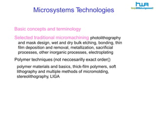
- 1. Microsystems Technologies Basic concepts and terminology Selected traditional micromachining photolithography and mask design, wet and dry bulk etching, bonding, thin film deposition and removal, metallization, sacrificial processes, other inorganic processes, electroplating Polymer techniques (not neccesarilly exact order() polymer materials and basics, thick-film polymers, soft lithography and multiple methods of micromolding, stereolithography, LIGA
- 2. Micro Stereolithography (μSL) Arapid prototyping microfabrication technique that involves layer by layer photopolymerization of resin to produce 3D microstructures. By exposing multiple layers, one on top of each other, complex 3D shapes can be realized. Book: Microstereolithography and other fabrication techniques for 3D MEMS, V. K. Varadan, et.al., John Wiley & Sons, 2001. Article: “Mail Order Microfluidics”, A.K.Au, et.al., Lab on a Chip, 2014, p 1294. Types Scanning method Scans across each layer line by line using a laser to photopolymerize one small “spot” at a time. Projection method Scans each layer all at once using projection of uv-light through a (dynamic) mask.
- 3. Micro-Stereolithography μSL fabrication steps 1. 2. CAD file generation Slicing 3D model into series of closely spaced horizontal planes (layers) representing the 2D (x-y) cross-sections 2D model translation into numerical control code for laser or dynamic mask 3. 4. Photopolymerization of successive layers to form the 3 the 3D (beam or projection) z y x object by building it up one layer at a time (z-dir) layers Layer-by-layer SEM photograph photopolymerization CAD drawing
- 4. Micro-Stereolithography μSL fabrication steps 1. 2. CAD file generation Slicing 3D model into series of closely spaced horizontal planes (layers) representing the 2D (x-y) cross-sections 2D model translation into numerical control code for laser or dynamic mask 3. 4. Photopolymerization of successive layers to form the 3D Object by building it up one layer at a time (z-dir) (beam or projection) z y x layers Layer-by-layer SEM photograph photopolymerization CAD drawing
- 5. Micro-Stereolithography Most common is HDDA: 1,6 hexanediol diacrylate. Acrylates Urethanes Epoxies Vinyl ethers Resolution and Typically not minimum feature great (even still; see 2014 article) Even using expensive equipment ଛ min. resolutions on order of 30 μm or ଛ smallest features on order of 100 μm so or so Materials for μSL
- 6. Micro-Stereolithography cellular scaffolds Examples and applications Fluidics
- 7. Two-Photon Polymerization (2PP) •Principle similar to stereo-lithography (SL) technique •Provides much better structural resolution and quality •Curing: 2PP uses near-infrared (IR) laser pulses whereas μSL uses ultraviolet (UV) laser radiation •Photosensitive materials are usually transparent in the infrared, highly absorptive in the UV range •initiate polymerization with IR laser pulses within the volume and fabricate 3D structures, where as UV is surface/planar Courtesy Laser Zentrum Hannover e.V
- 8. 3D Printing 3D printer general fabrication steps 1. CAD file generation 2. Slicing 3D model into series of closely spaced horizontal planes (layers) representing the 2D (x-y) cross-sections 3. 2D model translation into numerical control code for extruders that extrude as lines of polymer (1 to 4 typically) from filament the 4. Extruding of polymers and fusion of the printed lines Typical polymers (thermoplastics) acrylonitrile butadiene styrene (ABS) polycarbonate (PC) polylactic acid (PLA) high density polyethylene (HDPE) PC/ABS polyphenylsulfone (PPSU) polyurethane (PU) based elastomers
- 9. 3D Printing Resolution and minimum feature Typically not great, but getting better Equipment not so expensive though to get ೦ min. resolutions on order of 30 μm or so ೦ smallest features on order of 50 μm or so Example application in microfluids:packaging article (thanks Kimball!): O.H. Paydar, et.al., Sensors and Actuators A, 2014, p 199. made using Makerbot in my lab
- 10. Micromolding Micromold inserts Micro injection molding Micro hot embossing (compression molding, stamping) Soft lithography Casting of elastomeric structures Micro transfer molding MIMIC (micro molding in capillaries) Micro contact printing
- 11. Micromolding: Common Methods and Materials Molding method Molding material(s) Mold insert material(s) Injection molding Thermoplastics Nickel, silicon, SU-8, NiCo,WCo, steel, ceramic powder Hot embossing Thermoplastics Nickel, silicon, NiCo, WCo, steel Soft lithography: casting Thermosets, elastomers SU-8, silicon, silicon dioxide or nitride Micro transfer molding and MIMEC Thermosets PDMS Micro contact printing Self-assembled monolayers PDMS
- 12. Micromolding Micromold insert:general characteristics Low mechanical stiction and friction Vertical or positively sloped sidewalls (no undercut) Avoid surface oxidation chemically inert, smooth surfaces, homogeneous materials, free of sidewall defects Example micromold insert methods a) b) c) d) e) f) CNC physical milling Laser ablation X-ray litho and e-form Si etching SU-8 EDM (electro discharge machining)
- 13. Micro Injection Molding High-temperature micromolding technique using inserts Typical process 1. 2. 3. 4. 5. Mold inserts are placed into molding chamber Air is evacuated out leaving the chamber under vacuum Polymer pellets are heated above their melting point Liquid polymer is injected into the mold Pressure and temperature holding to ensure good filling of high-aspect ratio structures Cooling Demolding 6. 7.
- 14. Micro Injection Molding Typical specs 1. 2. Injection pressure set 500 – 2000 bar (high!) Molding temperatures above glass transition, below degradation Minimum wall thickness of 20 μm High aspect ratios (20+) Structural details down to 1 μm (typical) 3. 4. 5. Materials PMMA PSU PC PA POM PEEK COC and temperatures for μIM polymethylmethacrylate polysulfone polycarbonate polyamide polyoxymethalene polyethylethylketone cyclic olefin polymer (in ºF) 200-250 360-400 240-260 220-280 180-210 370-400 260-310
- 15. Micro Injection Molding Examples and applications microchannels AMANDA micropump cell chip LILLIPUT Microfluidic microneedles ChipShop
- 16. Micro Hot Embossing High pressure micromolding technique by compressing a softened polymer against a mold insert Also called stamping or compression molding Typical process 1. 2. 3. Mold inserts and polymer are placed into molding chamber Chamber is placed under vacuum Polymer thick film and mold are heated to just above glass transition temperature ଛ much lower temps than injection molding 4. Polymer thick film is pressed to fit into themold insert using pressures Tool and substrate are cooled (Re-embossing), demolding and part extraction high 5. 6.
- 17. Micro Hot Embossing Force, temparature in arbitrary units
- 18. Micro Hot Embossing Typical specs 1. 2. 3. 4. Typical pressure = 25 – 30 bars Submicron features possible Good aspect ratio possibilities (10-20:1) Simple and inexpensive Materials and glass transition temperature Abbreviation
- 19. Micro Hot Embossing Examples and applications 0.8 μm PMMAfeatures Microchannel arrays from DRIE silicon mold 150 μm Nano Devices and Systems Research biodegradable microneedles With fiber optics 50 μm Channel
- 20. Soft Lithography: PDMS Primer The “soft” in “soft lithography”: PDMS Poly dimethyl siloxane (“silicone rubber” elastomer) Good reference: Xia and Whitesides, SoftLithography, Annual Review Materials Science, 28 (1998) 153-84.
- 21. Soft Lithography: PDMS Primer Characteristics of PDMS 1. 2. Good chemical stability Not particularly hydroscopic (does not swell with humidity), however, many organic solvents will swell PDMS High gas permeability (for good or bad() Good thermal stability (up to 180 C) 3. 4. 5. Good thermal insulator (thermal conductivity 0.2W/mK, thermal expansion 310 μm/mC) Optically transparent down to 250 nm Durable Surface properties can be readily altered using plasma for sealing to other PDMS, silicon, silicon nitride, PS, PE Readily available, easy to work with Highly elastic (can be good or bad); E = 750 kPa Good insulator; breakdown voltage 2x10⁷ V/m Shrinks about 1% on curing Nontoxic and biocompatible 6. 7. 8. 9. 10. 11. 12. 13.
- 22. Soft Lithography Casting PDMS Master can be silanized by exposure to vapor: CF3(CF2)6(CH2)2SiCl3 for 30 minutes This attaches chlorosilane to any dangling surface bonds (e.g., OH), so they they will not attach to PDMS Master is usually silicon or SU-8 PDMS structures can be used directly, for another soft lithography process, or machined Cure (e.g., 65C 2 hours) for using other methods Features down to 30nm
- 23. Soft Lithography Molded tubing into PDMS Tubing is also silicone (Tygon) Soft lithography potential problems Sagging Shrinkage (1%) 0.2<h<20 0.5<d<200 0.5<l<200 (microns) Lateral displacement Sticking to master (pairing) Holes higher aspect ratio than towers possible
- 24. PDMS DeviceApplications Applications in PDMS Biochemical assays Capillary electrophoresis Cell counting and sorting Cell growth Cell studies using sheath mixer flow retina Chemical reactions Control of fluid flow cells Detection of biological species Mixing O-rings Genomics Liquid chromatography Mass spectrometry Optical components Implantable packaging Hybrid systems o-rings hybrid Goodreview: Sia and Whitesides, Electrophoresis 24 (2003), 3563-76.
- 25. Micro Transfer Molding Process Curing is either uv or thermal Typical materials: PU, epoxy, suspensions (sol gel) Feature sizes of a few microns Can build layers for multilevel structures Basic Process Multilayer Polyurethane (PU): thermosetting
- 26. Micro Transfer Molding Applications
- 27. Micro Molding in Capillaries Basic process PDMS mold is pressed tightly to substrate surface Common substrates: silicon, glass Liquid resin fills channels by capillary action Typical structure sizes: 350nm to 50 μm wide a few microns deep
- 28. Micro Contact Printing Introduction Uses a PDMS “stamp” to apply another material (self-assembled monolayer (SAM), biomolecules such as proteins) to the substrate in a pattern Stamp is contacted to substrate, which can be coated oxide or metal layers (e.g., Au, Ag) with Patterned material can then act as a resist for etching selective deposition or Features as small as 300 nm can be realized Difficult to pattern large area surfaces Can pattern non-planar surfaces (e.g., cylinders)
- 29. Micro Contact Printing First, make PDMS stamp using molding as we discussed Next apply “ink” which contains the SAM molecules or biomolecules in (e.g., ethanol) another solution apply “ink” “ink” Print the SAMS that have better or biomolecules affinity to substrate surface than PDMS selective deposition selective removal Use the monolayer directly or for selective etching or deposition of another material
- 30. Micro Contact Printing Self-assembled monolayers Alkanethiol CH3(CH2)n-1SH alkane is a hydrocarbon that is entirely thiol is a sulfhydryl group, SH single bonded, CH3(CH2)n-1 Layer thickness is controlled by the number of methyl groups, n SH has a selective affinity (likes to attach to) gold in particular Easy surface adsorption onto gold from solution Hydrophobic and not inert to cell/protein attachment on terminal end
- 31. Micro Contact Printing (Other SAMS) alkylsiloxanes on hydroxyl terminated surfaces (e.g., silicon dioxide and other glasses) SAMs used for making surface micromachined polysilicon hydrophobic to prevent stiction SAMS uses SAMs can be used directly as a “resist” or used to modify surface properties for additional molecular attachment Not resistive to RIE, only resistant to certain wet etching solutions (see Xia and Whitesides) Can also use SAMS for selective deposition; material will either attach selectively to SAMS template (polymers) or nucleate where there are no SAMS (CVD metal)
- 32. (Micro Contact Printing) (Examples of SAMS as a “resist”)
- 33. Micro Contact Printing Resist patterning on non-planar substrates Can easily pattern on cylinders Flexible PDMS can be deformed around non-planar substrate Can thus pattern metal on cylindrical objects such as glass fibers
- 34. Micro Contact Printing μCP patterned metal for electrodeposition After metal wet etching, electroplate Can also be used for non-planar substrates Make free-standing patterned metal by etching away substrate (e.g., glass tube)
- 35. Micro Contact Printing Examples and applications for μCP plus e-plating Microcoils for micro nuclear magnetic resonance (μNMR), microsolenoids, and microtransformers; microstents microstent solenoid ferromagnetic wire small insulting tube transformer
- 36. Micro Contact Printing Biomolecule and cell applications Direct biomolecule stamping (e.g., proteins) Attachment of cells or biomolecules to SAMS Potential uses: microarrays for biochemical analysis cell manipulation and research Hippocampal neurons on poly lysine (protein) printed surface
- 37. Micro Contact Printing (brain., spinal cord cells) Endothelial cells selectively cultured on SAMs on Au coated substrate (chemically alters EC function)