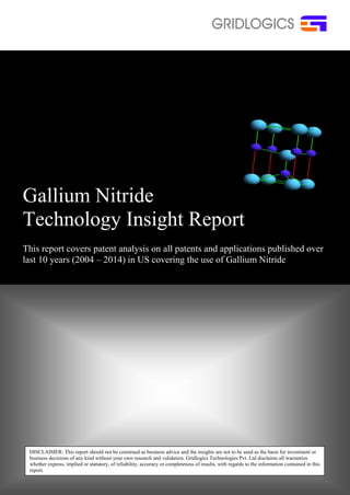
Gallium Nitride (GaN)

This report takes a look into the patenting activity around gallium Nitride uncovering the companies, inventors, and key applications. GaN is a binary III-V direct bandgap semiconductor commonly used in LEDs. Its wide-band gap of 3.4 eV affords its special properties for applications in optoelectronic, high-power and high-frequency devices. Because GaN offers very high breakdown voltages, high electron mobility, and saturation velocity it is also an ideal candidate for high-power and high-temperature microwave applications like RF power amplifiers at microwave frequencies and high-voltage switching devices for power grids. Solutions that use GaN-based RF transistors are also replacing the magnetrons used in microwave ovens. Gallium Nitride (GaN) transistor models have evolved from GaAs (gallium arsenide) transistor models; however there are many advantages GaN offers: • Higher operating voltage (over 100-V breakdown) • Higher operating temperature (over 150°C channel temperature) • Higher power density (5 to 30 W/mm) • Durable and crack-resistant material GaN devices are often grown on SiC (silicon carbide) substrates, but to achieve lower-cost GaN devices, they can be grown on sapphire and silicon wafers. GaN’s wide bandgap allows for higher breakdown voltages and operation at high temperatures. The high thermal conductivity of SiC makes it a better substrate than silicon for power amplifier applications that require good heat sinking.

Recomendados
Recomendados
Mais conteúdo relacionado
Mais procurados
Mais procurados (20)
Destaque
Destaque (14)
Semelhante a Gallium Nitride (GaN)
Semelhante a Gallium Nitride (GaN) (20)
Mais de Gridlogics
Mais de Gridlogics (20)
Último
Último (20)
Gallium Nitride (GaN)
- 1. Gallium Nitride Technology Insight Report This report covers patent analysis on all patents and applications published over last 10 years (2004 – 2014) in US covering the use of Gallium Nitride DISCLAIMER: This report should not be construed as business advice and the insights are not to be used as the basis for investment or business decisions of any kind without your own research and validation. Gridlogics Technologies Pvt. Ltd disclaims all warranties whether express, implied or statutory, of reliability, accuracy or completeness of results, with regards to the information contained in this report.
- 2. Introduction ............................................................................................................................................ 3 Technical Segmentation (Patent Categories) ......................................................................................... 5 IP Analysis ............................................................................................................................................... 6 Publication Trend .................................................................................................................................... 6 Top Companies ....................................................................................................................................... 7 Research activity around world .............................................................................................................. 8 Companies - Key Statistics ...................................................................................................................... 9 Inventor - Key Statistics ........................................................................................................................ 13 Company activity across crystal structures .......................................................................................... 19 Company activity across physical properties ........................................................................................ 21 Gallium Nitride – Application Areas vs. Crystal Structures ................................................................... 22 Landscape for Gallium Nitride applications ......................................................................................... 23 Analysis of significant companies within Gallium Nitride .................................................................... 24 Assignee Landscape around application areas and crystal structure .................................................. 25 Universities: Focus across Crystal structure, applications and physical properties .............................. 34 Appendix: Search Strings Used for Categorization ............................................................................... 39 Summary............................................................................................................................................... 44 Sources & References ........................................................................................................................... 46 Page 2 of 46 Table of Contents © 2014 Gridlogics. All Rights Reserved. Patent iNSIGHT Pro™ is a trademark of Gridlogics Technologies Pvt.LTD Feedbacks and Comments on this report can be sent to feedback_tr@patentinsightpro.com
- 3. GaN is a binary III-V direct bandgap semiconductor commonly used in LEDs. Its wide-band gap of 3.4 eV affords its special properties for applications in optoelectronic, high-power and high-frequency devices. Because GaN offers very high breakdown voltages, high electron mobility, and saturation velocity it is also an ideal candidate for high-power and high-temperature microwave applications like RF power amplifiers at microwave frequencies and high-voltage switching devices for power grids. Solutions that use GaN-based RF transistors are also replacing the magnetrons used in microwave ovens. Gallium Nitride (GaN) transistor models have evolved from GaAs (gallium arsenide) transistor models; however there are many advantages GaN offers: GaN devices are often grown on SiC (silicon carbide) substrates, but to achieve lower-cost GaN devices, they can be grown on sapphire and silicon wafers. GaN’s wide bandgap allows for higher breakdown voltages and operation at high temperatures. The high thermal conductivity of SiC makes it a better substrate than silicon for power amplifier applications that require good heat sinking. It is very hard, mechanically stable wide bandgap semiconductor material with high heat capacity and thermal conductivity. In its pure form it resists cracking and can be deposited in thin film on sapphire or silicon carbide, despite the mismatch in their lattice constants.GaN can be doped with silicon (Si) or with oxygen to n-type and with magnesium (Mg) to p-type; however, the Si and Mg atoms change the way the GaN crystals grow, introducing tensile stresses and making them brittle. Gallium nitride compounds also tend to have a high spatial defect frequency, on the order of a hundred million to ten billion defects per square centimeter. Overview of top companies involved in applications of gallium nitride and their publication Page 3 of 46 Higher operating voltage (over 100-V breakdown) Higher operating temperature (over 150°C channel temperature) Higher power density (5 to 30 W/mm) Durable and crack-resistant material © 2014 Gridlogics. All Rights Reserved. Patent iNSIGHT Pro™ is a trademark of Gridlogics Technologies Pvt.LTD Introduction This report covers: Feedbacks and Comments on this report can be sent to feedback_tr@patentinsightpro.com trend Focus on crystal structures, applications and physical properties of gallium nitride Trends for different applications of gallium nitride and their patent activity Analyzing key companies within gallium nitride
- 4. 257 Active Solid-State Devices (e.g., Transistors, Solid-State Diodes) 438 Semiconductor Device Manufacturing: Process 372 Coherent Light Generators 117 Single-crystal, oriented-crystal, and epitaxy growth processes; non-coating apparatus therefor TAC:((Gallium wd1 Nitride*) or "GaN" or "III/V semiconductor") The publications included in the report are updated as of 6th September, 2014 Page 4 of 46 Patent Search Strategy Using PatSeerfollowing searchquerywas usedto create patent set. TAC– Title, Abstract, ClaimsPBC– Publication Country PBY – Publication Year UC-US Classification © 2014 Gridlogics. All Rights Reserved. Patent iNSIGHT Pro™ is a trademark of Gridlogics Technologies Pvt.LTD Feedbacks and Comments on this report can be sent to feedback_tr@patentinsightpro.com AND PBC:US AND PBY:[2004 TO 2014] AND UC:(257* or 438* or 372* or 117*) The query was directed to search through title, abstract and claims and was limited to US publications published during last 10 years Result set of 7888 records with one publication per family (INPADOC Families) was generated and imported in Patent iNSIGHT Pro Definitions to US Classifications
- 5. Crystal Structure Applications Physical Properties Metalorganic CVD N-Type P-Type The categorization involved defining a search strategy for each topic and then conducting the search using the Advanced Searching capability in Patent iNSIGHT Pro. Details of search strings used for each category are given in Appendix. Page 5 of 46 Technical Segmentation (Patent Categories) Amplifiers Artificial Lighting Automobile Aviation Biological Sensors Blue Lighting Blue Ray Clean Energy Defence Detector Displays Flash Memory Food Fuel Cells High Electron Mobility Transistor High Resolution Printing Hybrid Vehicle Inverter Laser Diodes Laser Printer LED MMIC Mobile Phone Modulator MOSFET Nanotech for Medicines Nanotubes Optoelectronics Photodiode Radar Satellite Communication Solar Cells Thin Film Batteries © 2014 Gridlogics. All Rights Reserved. Rock Salt Wurtzite Zinc -Blende Patent iNSIGHT Pro™ is a trademark of Gridlogics Technologies Pvt.LTD Feedbacks and Comments on this report can be sent to feedback_tr@patentinsightpro.com
- 6. It can be seen that publications for GaN are constantly rising from 2009 with the real surge in the activity around this technology has happened since 2012. It’s clear the current activity around these technologies is likely to continue seeing more innovation in the near future. Once the patents were populated in Patent iNSIGHT Pro, the publication trend chart was generated on a single click using the dashboard tool. Page 6 of 46 © 2014 Gridlogics. All Rights Reserved. Publication Trend Patent iNSIGHT Pro™ is a trademark of Gridlogics Technologies Pvt.LTD IP Analysis How we did it? Feedbacks and Comments on this report can be sent to feedback_tr@patentinsightpro.com
- 7. Note: Records for Matsushita Electrical Ind Co Ltd have not been grouped with Panasonic Corp in spite of their merger with Panasonic, as some of the patents owned by both these companies have not been transferred to a single company. 11. TAIWAN SEMICONDUCTOR MFG LTD 12. SOITEC 13. SONY CORP 14. EPISTAR CORP 15. INTERNATIONAL RECTIFIER CORP 16. FUJITSU LTD 17. ROHM CO LTD 18. MITSUBISHI ELECTRIC CORP 19. INFINEON TECHNOLOGIES AG 20. APPLIED MATERIALS INC 1. SAMSUNG GROUP 2. SUMITOMO ELECTRIC IND CO LTD 3. TOSHIBA CORP 4. TOYODA GOESI CO LTD 5. PANASONIC CORP 6. LG INNOTEK CO LTD 7. CREE INC 8. SHARP CORP 9. UNIV CALIFORNIA 10. OSRAM AG Once the patents were populated in Patent iNSIGHT Pro, the assignee clean- up tools were used to normalize the names. Different cleanup tools were leveraged: • To locate assignees for unassigned records • To clean up records having multiple assignees • To locate the correct assignee names for US records using the US assignments database • To merge assignees that resulted from a merger or acquisition or name change. The dashboard tool within Patent iNSIGHT Pro was used to find the top 20 assignees within the given patent set. A visual graph was created based on the results of the top assignees with the number of patents alongside each one. Thecomplete Assignee table in available in the following Excel file: http://www.patentinsightpro.com/techreports/0914/List%20of%20Assignees.xls Page 7 of 46 © 2014 Gridlogics. All Rights Reserved. Top Companies The top organizationsare: Patent iNSIGHT Pro™ is a trademark of Gridlogics Technologies Pvt.LTD How we did it? Feedbacks and Comments on this report can be sent to feedback_tr@patentinsightpro.com
- 8. In terms of regional pockets where patent protection is being sought most frequently for these technologies, USleads the count, followed by the JPand KR. The table below ranks top priority countries and helps provide an indication of where innovation in this area is originating: The map was generated using the Priority country coverage map option provided in the dashboard tool within Patent iNSIGHT Pro. Page 8 of 46 Research activity around world © 2014 Gridlogics. All Rights Reserved. Patent iNSIGHT Pro™ is a trademark of Gridlogics Technologies Pvt.LTD How we did it? Feedbacks and Comments on this report can be sent to feedback_tr@patentinsightpro.com Country Code Total US 3237 JP 2515 KR 969 TW 403 DE 228
- 9. Here we summarize key parameters of Top 15 companies such as filing trend, Top inventors in each company and Coverage of underlying patent families Page 9 of 46 Companies - Key Statistics © 2014 Gridlogics. All Rights Reserved. Patent iNSIGHT Pro™ is a trademark of Gridlogics Technologies Pvt.LTD Feedbacks and Comments on this report can be sent to feedback_tr@patentinsightpro.com Assignee Total No. of Record s Filing Trend (Absolute) Filing Year Range Key Inventor (Top 5) Co- Assignees Coverage (Includes families) US WO JP DE FR CN AU CA KR IN SAMSUNG GROUP 538 (6.8%) 1999- 2014 LEE JAE HOON(41) OH JAE-JOON( 23) JANG EUN JOO(21) SHIN JAI-KWANG( 21) KIM JE WON(19) JUN SHIN AE(1) KUMOH NAT INST TECH(1) 535 12 291 30 1 150 2 1 476 0 SUMITOM O ELECTRIC IND CO LTD 307 (3.9%) 2003- 2014 UENO MASAKI(71) KYONO TAKASHI(60) YOSHIZUMI YUSUKE(58) AKITA KATSUSHI(56) ENYA YOHEI(47) SONY CORP(2) SHARP CORP(1) TOYODA GOSEI CO LTD(1) 307 137 266 23 0 204 1 30 148 0 TOSHIBA CORP 261 (3.3%) 2001- 2014 NUNOUE SHINYA(55) TACHIBANA KOICHI(22) TANAKA AKIRA(17) HIKOSAKA TOSHIKI(16) NAGO HAJIME(16) SANDISK 3D LLC(1) 261 44 222 3 0 62 0 1 52 0 TOYODA GOSEI CO LTD 226 (2.9%) 1996- 2014 MIKI HISAYUKI(32) SHIBATA NAOKI(21) OKUNO KOJI(18) NAGAI SEIJI(16) YAMAZAKI SHIRO(15) LEUCHSTO FF BREITUNGE N GMBH(1) LITEC GBR(1) SUMITOM O ELECTRIC IND CO LTD(1) TRIDONIC OPTOELECT 225 86 154 20 0 89 8 0 51 1
- 10. Page 10 of 46 RONICS GMBH(1) © 2014 Gridlogics. All Rights Reserved. Patent iNSIGHT Pro™ is a trademark of Gridlogics Technologies Pvt.LTD Feedbacks and Comments on this report can be sent to feedback_tr@patentinsightpro.com PANASON IC CORP 201 (2.5%) 2001- 2014 UEDA TETSUZO(57) YOKOGAWA TOSHIYA(56) KATO RYOU(21) TANAKA TSUYOSHI(20) YAMADA ATSUSHI(18) No Co- Assignee Present 201 119 139 4 0 100 1 0 15 4 LG INNOTEK CO LTD 178 (2.3%) 2002- 2014 SONG JUNE O(16) SON HYO KUN(15) LEE SUK HUN(13) JEONG HWAN HEE(13) KANG DAE SUNG(9) No Co- Assignee Present 177 63 54 10 0 107 7 5 151 9 CREE INC 172 (2.2%) 2002- 2014 SAXLER ADAM WILLIAM(23) WU YIFENG(16) PARIKH PRIMIT(13) BERGMANN MICHAEL JOHN(12) SHEPPARD SCOTT T(11) No Co- Assignee Present 171 111 107 23 0 58 18 39 53 7 SHARP CORP 159 (2%) 2000- 2014 ITO SHIGETOSHI(2 1) KAMIKAWA TAKESHI(19) TSUDA YUHZOH(14) HEFFERNAN JONATHAN(13 ) HOOPER STEWART EDWARD(13) SUMITOM O ELECTRIC IND CO LTD(1) 159 38 115 3 0 70 5 0 12 2 UNIV CALIFORN IA 147 (1.9%) 2001- 2014 DENBAARS STEVEN P(71) NAKAMURA SHUJI(69) SPECK JAPAN SCIENCE & TECH AGENCY(10 ) 147 113 61 0 0 26 13 7 49 2
- 11. Page 11 of 46 JAMES(54) MISHRA UMESH K(23) SATO HITOSHI(10) © 2014 Gridlogics. All Rights Reserved. Patent iNSIGHT Pro™ is a trademark of Gridlogics Technologies Pvt.LTD Feedbacks and Comments on this report can be sent to feedback_tr@patentinsightpro.com OSRAM AG 136 (1.7%) 2000- 2013 HAERLE VOLKER(40) HAHN BERTHOLD(27) STRAUSS UWE(18) EISERT DOMINIK(17) LELL ALFRED(11) FREIBERGE R COMPOUN D MATERIALS GMBH(1) 136 102 108 110 1 78 1 3 58 0 TAIWAN SEMICON DUCTOR MFG LTD 128 (1.6%) 2004- 2014 YU CHUNG-YI( 22) CHEN CHI-MING( 21) YU JIUN-LEI JERRY(18) YAO FU-WEI( 17) CHEN DING-YUAN( 16) No Co- Assignee Present 122 3 9 3 0 80 0 0 22 0 SOITEC 115 (1.5%) 2003- 2014 ARENA CHANTAL(25) LETERTRE FABRICE(24) GHYSELEN BRUNO(17) FAURE BRUCE(14) WERKHOVEN CHRISTIAAN J(10) COMMISSA RIAT A LENERGIE ATOMIQUE (2) 115 62 56 15 48 56 4 0 52 0 SONY CORP 111 (1.4%) 2000- 2014 OKUYAMA HIROYUKI(20) BIWA GOSHI(19) OOHATA TOYOHARU(18 ) DOI MASATO(15) KURAMOTO MASARU(14) SUMITOM O ELECTRIC IND CO LTD(2) UNIV TOHOKU(2) SONY SHIROISHI SEMICOND UCTOR INC(1) 111 21 99 6 0 61 3 1 33 0 EPISTAR CORP 96 (1.2%) 1999- 2014 HSIEH MIN-HSUN( 24) YAO CHIU-LIN( 9) No Co- Assignee Present 96 0 24 15 0 4 0 0 7 0
- 12. Page 12 of 46 HSU TA-CHENG( 9) LIU WEN-HUANG( 9) OU CHEN(9) © 2014 Gridlogics. All Rights Reserved. Patent iNSIGHT Pro™ is a trademark of Gridlogics Technologies Pvt.LTD Feedbacks and Comments on this report can be sent to feedback_tr@patentinsightpro.com INTERNAT IONAL RECTIFIER CORP 95 (1.2%) 2001- 2014 BEACH ROBERT(22) BRIERE MICHAEL A(21) BRIDGER PAUL(9) KINZER DANIEL M(6) PINER EDWIN L(6) No Co- Assignee Present 95 33 52 17 1 6 2 0 7 0 How we did it? From the Assignee 360° report options, we selected Top 15 Assignees and the different pieces of information we wanted to include in the singular display and then ran the report. The generated report was then exported to Excel using the option provided for the same.
- 13. Here we summarize key parameters of Top 15 Inventors such as filing trend, key associated companies and top 5 co-inventors. Co-Inventors Page 13 of 46 Inventor - Key Statistics Filing Trend ( Absolute ) Filing Year Range Key Assignees (Top 5) © 2014 Gridlogics. All Rights Reserved. Total No. of Records Patent iNSIGHT Pro™ is a trademark of Gridlogics Technologies Pvt.LTD Inventor NAKAMURA Feedbacks and Comments on this report can be sent to feedback_tr@patentinsightpro.com SHUJI 91 (1.2%) 2001- 2014 UNIV CALIFORNIA(69) JAPAN SCIENCE & TECH AGENCY(13) NICHIA CORP(8) CREE INC(5) SORAA INC(3) DENBAARS STEVEN P(67) SPECK JAMES(47) SATO HITOSHI(11) FEEZELL DANIEL F(10) IZA MICHAEL(9) DENBAARS STEVEN P 76 (1%) 2005- 2014 UNIV CALIFORNIA(71) JAPAN SCIENCE & TECH AGENCY(9) CREE INC(2) BAKER TROY J(1) DENBAARS STEVEN P(1) NAKAMURA SHUJI(67) SPECK JAMES(48) SATO HITOSHI(10) IZA MICHAEL(9) MISHRA UMESH K(9) UENO MASAKI 71 (0.9%) 2004- 2014 SUMITOMO ELECTRIC IND CO LTD(71) SONY CORP(1) YOSHIZUMI YUSUKE(51) ENYA YOHEI(45) KYONO TAKASHI(44) SUMITOMO TAKAMICHI(32) AKITA KATSUSHI(25) UEDA TETSUZO 66 (0.8%) 2000- 2014 PANASONIC CORP(57) MATSUSHITA ELECTRICAL IND CO LTD(9) CBL TECHNOLOGIES INC(1) UEDA DAISUKE(15) HIKITA MASAHIRO(14) TANAKA TSUYOSHI(14) UEMOTO YASUHIRO(10) TAKIZAWA TOSHIYUKI(8) YOKOGAWA TOSHIYA 64 (0.8%) 2002- 2014 PANASONIC CORP(56) MATSUSHITA ELECTRICAL IND CO LTD(8) KATO RYOU(21) YAMADA ATSUSHI(19) INOUE AKIRA(18) FUJIKANE MASAKI(13) ISHIBASHI AKIHIKO(13)
- 14. DENBAARS STEVEN P(48) NAKAMURA SHUJI(47) TYAGI ANURAG(8) HASKELL BENJAMIN A(7) MISHRA UMESH K(7) UENO MASAKI(44) ENYA YOHEI(43) YOSHIZUMI YUSUKE(42) AKITA KATSUSHI(34) SUMITOMO TAKAMICHI(33) UENO MASAKI(51) KYONO TAKASHI(42) ENYA YOHEI(40) SUMITOMO TAKAMICHI(32) AKITA KATSUSHI(26) KYONO TAKASHI(34) YOSHIZUMI YUSUKE(26) UENO MASAKI(25) ENYA YOHEI(24) SUMITOMO TAKAMICHI(20) TOSHIBA CORP(55) TACHIBANA KOICHI(22) HIKOSAKA TOSHIKI(16) NAGO HAJIME(16) SUGIYAMA NAOHARU(16) SAITO SHINJI(13) Page 14 of 46 2005- 2014 UNIV CALIFORNIA(54) JAPAN SCIENCE & TECH AGENCY(9) SORAA INC(5) SEOUL VIOSYS CO LTD(1) SEOUL SEMICONDUCTOR CO LTD(1) 2004- 2012 SUMITOMO ELECTRIC IND CO LTD(60) SONY CORP(1) 2007- 2013 SUMITOMO ELECTRIC IND CO LTD(58) 2003- 2013 SUMITOMO ELECTRIC IND CO LTD(56) 2006- 2014 © 2014 Gridlogics. All Rights Reserved. 63 (0.8%) 60 (0.8%) 58 (0.7%) 56 (0.7%) 55 (0.7%) Patent iNSIGHT Pro™ is a trademark of Gridlogics Technologies Pvt.LTD SPECK JAMES KYONO TAKASHI YOSHIZUMI YUSUKE AKITA KATSUSHI NUNOUE SHINYA BOUR DAVID Feedbacks and Comments on this report can be sent to feedback_tr@patentinsightpro.com P 48 (0.6%) 1998- 2014 AVOGY INC(25) AVAGO TECHNOLOGIES GENERAL IP PTE LTD(7) PALO ALTO RESEARCH CENTER INCORPORATED(6) XEROX CORP(4) AVAGO TECHNOLOGIES ECBU IP (SINGAPORE) PTE LTD(1) KIZILYALLI ISIK C(25) NIE HUI(25) PRUNTY THOMAS R(22) BROWN RICHARD J(21) EDWARDS ANDREW P(18)
- 15. UENO MASAKI(45) KYONO TAKASHI(43) YOSHIZUMI YUSUKE(40) SUMITOMO TAKAMICHI(33) AKITA KATSUSHI(24) NIE HUI(36) BROWN RICHARD J(27) BOUR DAVID P(25) EDWARDS ANDREW P(23) PRUNTY THOMAS R(23) Page 15 of 46 2009- 2013 SUMITOMO ELECTRIC IND CO LTD(47) SONY CORP(1) 2007- 2014 AVOGY INC(37) ALTA DEVICES INC(2) EPOWERSOFT INC(2) INTERNATIONAL RECTIFIER CORP(2) © 2014 Gridlogics. All Rights Reserved. 47 (0.6%) 43 (0.5%) Patent iNSIGHT Pro™ is a trademark of Gridlogics Technologies Pvt.LTD ENYA YOHEI KIZILYALLI ISIK C Feedbacks and Comments on this report can be sent to feedback_tr@patentinsightpro.com LEE JAE HOON 41 (0.5%) 2004- 2014 SAMSUNG GROUP(41) OH JEONG TAK(7) LEE JUNG HEE(6) CHOI HEE SEOK(5) KIM KI SE(5) LEE SU YEOL(5) NIE HUI 41 (0.5%) 2011- 2014 AVOGY INC(38) EPOWERSOFT INC(2) BROWN RICHARD J(1) EDWARDS ANDREW P(1) KIZILYALLI ISIK C(1) KIZILYALLI ISIK C(36) BROWN RICHARD J(29) BOUR DAVID P(25) PRUNTY THOMAS R(24) EDWARDS ANDREW P(23) How we did it? From the Inventor 360° report options, we selected the different pieces of information we wanted to include in the singular display and then ran the report. The generated report was then exported to Excel using the option provided for the same.
- 16. Filing Trend of Patents across Top 15 US Classifications The chart shows the spread of patenting activity across various subclasses of technologies corresponding to US Class. The brown trend line associated with US Class 257/76 {Active solid-state devices with - Specified Wide Band Gap (1.5ev)}shows an impressive spike from 2009 onwards. In the chart, it can be seen that US Class 257/76and 257/98 are most favored subclasses under which 1048 and 721 patents have been categorized respectively. These arefollowed by 257/13, 257/103, 438/478, 257/79 under which 628, 601, 526,467patents have been categorized respectively. Once the patents were populated in Patent iNSIGHT Pro, the filing trend chart for top 15 US full classeswas generated on a single click using the dashboard tool. Page 16 of 46 © 2014 Gridlogics. All Rights Reserved. Patent iNSIGHT Pro™ is a trademark of Gridlogics Technologies Pvt.LTD How we did it? Feedbacks and Comments on this report can be sent to feedback_tr@patentinsightpro.com
- 17. - thin active physical layer which is (1) an active potential well layer thin enough to establish discrete quantum energy levels or (2) an active barrier layer thin enough to permit quantum mechanical tunneling or (3) an active layer thin enough to permit carrier transmission with substantially no scattering (e.g., superlattice quantum well, or ballistic transport device) -- Heterojunction --- Incoherent Light Emitter - Incoherent Light Emitter Structure -- With reflector, opaque mask, or optical element (e.g., lens, optical fiber, index of refraction matching layer, luminescent material layer, filter) integral with device or device enclosure or package - Making Device Or Circuit Emissive Of Nonelectrical Signal -- Including integrally formed optical element (e.g., reflective layer, luminescent material, contoured surface, etc.) - Heterojunction Device -- Field effect transistor --- Doping on side of heterojunction with lower carrier affinity (e.g., high electron mobility transistor (HEMT)) - Specified Wide Band Gap (1.5ev) Semiconductor Material Other Than Gaasp Or Gaalas - formation of semiconductive active region on any substrate (e.g., fluid growth, deposition) Page 17 of 46 Definitions to US Classifications used for above analysis US Class Definition 257/103 Active solid-state devices (e.g., transistors, solid-state diodes) - Incoherent Light Emitter Structure -- With particular semiconductor material 257/13 Active solid-state devices (e.g., transistors, solid-state diodes) 257/94 Active solid-state devices (e.g., transistors, solid-state diodes) - Incoherent Light Emitter Structure -- With heterojunction 257/98 Active solid-state devices (e.g., transistors, solid-state diodes) 438/22 Semiconductor device manufacturing: process - Making Device Or Circuit Emissive Of Nonelectrical Signal 438/29 Semiconductor device manufacturing: process 257/194 Active solid-state devices (e.g., transistors, solid-state diodes) 257/76 Active solid-state devices (e.g., transistors, solid-state diodes) 257/99 Active solid-state devices (e.g., transistors, solid-state diodes) - Incoherent Light Emitter Structure -- With housing or contact structure 438/478 Semiconductor Device Manufacturing: Process 438/46 Semiconductor device manufacturing: process - Making Device Or Circuit Emissive Of Nonelectrical Signal -- Compound semiconductor 438/47 Semiconductor device manufacturing: process - Making Device Or Circuit Emissive Of Nonelectrical Signal -- Compound semiconductor --- Heterojunction 257/79 Active solid-state devices (e.g., transistors, solid-state diodes) - Incoherent Light Emitter Structure © 2014 Gridlogics. All Rights Reserved. Patent iNSIGHT Pro™ is a trademark of Gridlogics Technologies Pvt.LTD Feedbacks and Comments on this report can be sent to feedback_tr@patentinsightpro.com
- 18. - Processes Or Apparatus Adapted For Manufacture Or Treatment Of Semiconductor Or Solid-State Devices Or Of Parts Thereof (EPO) -- Manufacture or treatment of semiconductor device (EPO) --- Device having at least one potential-jump barrier or surface barrier, e.g., PN junction, depletion layer, carrier concentration layer (EPO) ---- Device having semiconductor body comprising Group IV elements or Group III-V compounds with or without impurities, e.g., doping materials (EPO) ----- Multistep processes for manufacture of device using quantum interference effect, e.g., electrostatic Aharonov-Bohm effect (EPO) - Processes Or Apparatus Adapted For Manufacture Or Treatment Of Semiconductor Or Solid-State Devices Or Of Parts Thereof (EPO) -- Manufacture or treatment of semiconductor device (EPO) --- Device having at least one potential-jump barrier or surface barrier, e.g., PN junction, depletion layer, carrier concentration layer (EPO) ---- Device having semiconductor body comprising Group IV elements or Group III-V compounds with or without impurities, e.g., doping materials (EPO) ----- Deposition of semiconductor material on substrate, e.g., epitaxial growth, solid phase epitaxy (EPO) Page 18 of 46 257/E21.089 Active solid-state devices (e.g., transistors, solid-state diodes) 257/E21.09 Active solid-state devices (e.g., transistors, solid-state diodes) © 2014 Gridlogics. All Rights Reserved. Patent iNSIGHT Pro™ is a trademark of Gridlogics Technologies Pvt.LTD Feedbacks and Comments on this report can be sent to feedback_tr@patentinsightpro.com
- 19. The chart below shows research activity of companies across different crystal structures. Univ California has research activity across all types of crystal structures.Intel and Corning focus only on Wurtzite. First various crystal structureswere identified by manual research. Then by using a combination of semantic analysis tools such as clustering tools and searching tools available in Patent iNSIGHT Pro, records were categorized under structures. A co-occurrence matrix was generated using the co-occurrence analyzer to map the different structures with assignees. The matrix was filtered for top 20assignees and was converted into column chart using the option provided in software for the same. Page 19 of 46 Company activity acrossCrystal Structures © 2014 Gridlogics. All Rights Reserved. Patent iNSIGHT Pro™ is a trademark of Gridlogics Technologies Pvt.LTD How we did it? Feedbacks and Comments on this report can be sent to feedback_tr@patentinsightpro.com
- 20. The chart below shows research activity of companies across different applications. Cree leads in research around high electron mobility transistors and defence with 82 and 28 records respectively. Samsung and Univ California are the only companies focusing on high resolution printing with 9 and 7 records respectively. First various applications were identified by manual research. Then by using a combination of semantic analysis tools such as clustering tools and searching tools available in Patent iNSIGHT Pro, records were categorized under different applications. A co-occurrence matrix was generated using the co-occurrence analyzer to map the different applications with assignees. The matrix was filtered for the top 20 assignees and was converted into bubble chart using the option provided in software for the same. Page 20 of 46 Company activity across Applications © 2014 Gridlogics. All Rights Reserved. Patent iNSIGHT Pro™ is a trademark of Gridlogics Technologies Pvt.LTD How we did it? Feedbacks and Comments on this report can be sent to feedback_tr@patentinsightpro.com
- 21. The chart below shows research activity of companies across different physical properties. Avogy focuses only in N-type.Panasonic leads in research across P-type. Sumitomo has fairly comparable portfolio across all the physical properties. First various physical propertieswere identified by manual research. Then by using a combination of semantic analysis tools such as clustering tools and searching tools available in Patent iNSIGHT Pro, records were categorized under different properties. A co-occurrence matrix was generated using the co-occurrence analyzer to map the different properties with assignees. The matrix was filtered for the top 20assignees and converted into clustered column chart using the option provided in software for the same. Page 21 of 46 Company activity acrossPhysical Properties © 2014 Gridlogics. All Rights Reserved. Patent iNSIGHT Pro™ is a trademark of Gridlogics Technologies Pvt.LTD How we did it? Feedbacks and Comments on this report can be sent to feedback_tr@patentinsightpro.com
- 22. Gallium Nitride – Application Areas vs.Crystal Structures In the map, each structure is connected through links whose thickness and color intensity is directly proportional to the number of records relating them. The number (in red) next to each line represents the number of records present in a particular crystal structure and application areas. It can be seen Wurtzite crystal structure is used in more number of applications as compared to other crystal structures. Aviation,Defenceand Satellite industry industries use onlyWurtzite and Zinc Blende crystal structures. Note: Orange nodes represent the crystal structure, whereas purple nodes refer toapplication areas. The clusters that were created for previous analysis were correlated using the co‐occurrence analyzer and the resulting matrix wasrepresented as Correlation map. Also, links between same field types were removed using the option provided. Page 22 of 46 © 2014 Gridlogics. All Rights Reserved. Patent iNSIGHT Pro™ is a trademark of Gridlogics Technologies Pvt.LTD How we did it? Feedbacks and Comments on this report can be sent to feedback_tr@patentinsightpro.com
- 23. The contour map below represents key concepts for different applications of Gallium Nitridewith respect to complete patent portfolio. Clusters for photo diode and photo detector appearcloser to each other as they share high contextual and conceptual similarity between them. The nodes were coloured by companies. The VizMAP tool in Patent iNSIGHT Pro was used for this analysis. First the clusters for differentapplications were loaded on the map. They were analyzed on basis of their contextual similarity using title, abstract and claims as Text from the ‘Context mode’ option. We removed unrelated patents using the “Hide Unrelated records” option and one patent assignee using the options available in VizMAP. Page 23 of 46 Landscape for Gallium Nitride applications © 2014 Gridlogics. All Rights Reserved. Patent iNSIGHT Pro™ is a trademark of Gridlogics Technologies Pvt.LTD How we did it? Feedbacks and Comments on this report can be sent to feedback_tr@patentinsightpro.com
- 24. Analysis of significant companies within Gallium Nitride The chart shows research activity of significant companies in different application areas. It can be seen Triquint leads in research across satellite communication and has records present across most of the applications. Kymaand NXP are the only companies in biological sensors and inverter. We first created a group for companies focusing primarily around research around gallium nitride using autofilter option. Using co-occurrence analyzer, we used that group as data filter to generate a matrix for those companies with respect to applications and resulting matrix was converted to a stacked column chart. Page 24 of 46 © 2014 Gridlogics. All Rights Reserved. Application areas Patent iNSIGHT Pro™ is a trademark of Gridlogics Technologies Pvt.LTD How we did it? Feedbacks and Comments on this report can be sent to feedback_tr@patentinsightpro.com
- 25. Assignee Landscape around application areas and crystal structure The following table shows different applications and type of crystal structures used, but with the companies behind the records. It can be seen Laser Diode has maximum number of individual companies (24) with wurtzite as crystal structure. Crystal Structure (Column) Total Wurtzite Zinc-Blende Rock Salt Applications (Row) Total 109 56 34 36 ELOP ELECTROOPTICS IND LTD; GENERAL ELECTRIC CO; IPCO LLC; LOS ALAMOS NATIONAL SECURITY LLC; MITSUBISHI CHEM CORP; MOMENTIVE PERFORMANCE MATERIALS INC; PRESIDENT AND FELLOWS OF HARVARD COLLEGE; SORAA INC; TECHNION RES & DEV FOUNDATION; TECHNION RESEARCH AND DEVELOPEMENT FOUNDATION LTD; THE BOEING CO GENERAL ELECTRIC CO; GOVT OF USA AS REPRESENTED BY THE SECRETARY OF COMMERCE THE Page 25 of 46 ALCATEL LUCENT SA; COMMISSARIAT A LENERGIE ATOMIQUE; COVALENT MATERIALS CORP; CRYSTAL IS INC; FONDAZIONE ISTITUTO ITALIANO DI TECNOLOGIA; MITSUBISHI ELECTRIC CORP; NANOSYS INC; NATIONAL INST OF ADVANCED INDUSTRIAL SCIENCE AND TECHNOLOGY; NATIONAL SUN YAT-SEN UNIV; NATIONAL TSING HUA UNIV; ONED MATERIAL LLC; PHOSTEK INC; PRESIDENT AND FELLOWS OF HARVARD COLLEGE; SEOUL SEMICONDUCTOR CO LTD; SIXPOINT MATERIALS INC; SOITEC; SOUTHERN TAIWAN UNIV OF TECHNOLOGY; SUNG CHIEN-MIN; UNIV CALIFORNIA; UNIV CONNECTICUT; UNIV ILLINOIS; UNIV OF FLORIDA RESEARCH FOUNDATION INC AMBERWAVE SYSTEMS CORP; HARVATEK CORP; HONG KONG APPLIED SCIENCE AND TECHNOLOGY RESEARCH INSTCO LTD; KENDALL DON L.; NASA; NM SPINTRONICS AB; OHIO UNIV; QINETIQ LTD; RICOH CO LTD; SORAA INC; TAIWAN SEMICONDUCTOR MFG LTD; TOPCO SCIENTIFIC CO LTD; UNIV CALIFORNIA; UNIV UTAH RES FOUND; UNIV OF FLORIDA RESEARCH FOUNDATION INC; VTERA TECHNOLOGY INC AGENCY FOR SCIENCE TECHNOLOGY AND RESEARCH; CORNING INC; COVALENT MATERIALS CORP; CRYSTAL ISINC; AMBERWAVE SYSTEMS CORP; BINOPTICS CORP; NASA; OHIO UNIV; © 2014 Gridlogics. All Rights Reserved. Patent iNSIGHT Pro™ is a trademark of Gridlogics Technologies Pvt.LTD LED 45 Laser Diodes 43 Feedbacks and Comments on this report can be sent to feedback_tr@patentinsightpro.com
- 26. NATIONAL INST OF STANDARDS AND TECHNOLOGY; LG INNOTEK CO LTD; MITSUBISHI CHEM CORP; MOMENTIVE PERFORMANCE MATERIALS INC; PANASONIC CORP; RENSSELAER POLYTECH INST; UNIV NAT CHIAO TUNG ELMHURST RES INC; FRAUNHOFER-GESELLSCHAFT Page 26 of 46 DONGGUK UNIV INDUSTRY ACADEMIC COOPERATION FOUNDATION; FORSCHUNGSVERBUND BERLIN E.V.; MICRON TECHNOLOGY INC; MITSUBISHI ELECTRIC CORP; NATIONAL SUN YAT-SEN UNIV; NATIONAL TSING HUA UNIV; NICHIA CORP; PANASONIC CORP; SAINT-GOBAIN CERAMICS PLASTICS INC; SAMSUNG GROUP; SEIKO EPSON CORP; SEOUL SEMICONDUCTOR CO LTD; SIXPOINT MATERIALS INC; SOITEC; SUMITOMO ELECTRIC IND CO LTD; THE ROYAL INSTITUTION FOR THE ADVANCEMENT OF LEARNING / MCGILL UNIV; THE UNIV OF NOTRE DAME DU LAC; UNIV CALIFORNIA; UNIV ILLINOIS; UNIV NAT CHIAO TUNG QINETIQ LTD; RICOH CO LTD; SHARP CORP; SORAA INC; SUMITOMO ELECTRIC IND CO LTD; TAIWAN SEMICONDUCTOR MFG LTD; TOSHIBA CORP; UNIV CALIFORNIA; UNIV OF FLORIDA RESEARCH FOUNDATION INC; UNIV OF SEOUL INDUSTRY COOPERATION FOUNDATION; WISCONSIN ALUMNI RESEARCH FOUNDATION FONDAZIONE ISTITUTO ITALIANO DI TECNOLOGIA; IBM CORP; INTELLECTUAL DISCOVERY CO LTD; NANOSYS INC; ONED MATERIAL LLC; PHOSTEK INC; POSTECH ACAD IND FOUND; SEOUL SEMICONDUCTOR CO LTD; SIXPOINT MATERIALS INC; SOITEC; SUNG CHIEN-MIN; SVT ASSOCIATES INC; THE ROYAL INSTITUTION FOR THE ADVANCEMENT OF LEARNING / MCGILL UNIV; UNIV CALIFORNIA; UNIV ILLINOIS; UNIV NAT CHIAO TUNG; UNIV OF FLORIDA RESEARCH HONG KONG APPLIED SCIENCE AND TECHNOLOGY RESEARCH INSTCO LTD; TAIWAN SEMICONDUCTOR MFG LTD; UNIV CALIFORNIA; UNIV UTAH RES FOUND; UNIV OF SEOUL INDUSTRY COOPERATION FOUNDATION © 2014 Gridlogics. All Rights Reserved. Patent iNSIGHT Pro™ is a trademark of Gridlogics Technologies Pvt.LTD Solar Cells 36 Feedbacks and Comments on this report can be sent to feedback_tr@patentinsightpro.com ZUR FOERDERUNG DER ANGEWANDTEN FORSCHUNG E.V.; GOVT OF USA AS REPRESENTED BY THE SECRETARY OF COMMERCE THE NATIONAL INST OF STANDARDS AND TECHNOLOGY; INTERUNIV MICROELECTRONICS CENTRE VZW ; IPCO LLC; LOS ALAMOS NATIONAL SECURITY LLC; MOMENTIVE PERFORMANCE MATERIALS INC;
- 27. FOUNDATION INC Q1 NANOSYSTEMS CORP; RENSSELAER POLYTECH INST; SAMSUNG GROUP; SORAA INC; STICHTING IMEC NEDERLAND; TECHNION RESEARCH AND DEVELOPEMENT FOUNDATION LTD; THE BOEING CO; UNIV NAT CHIAO TUNG; WILLIAM MARSH RICE UNIV ELMHURST RES INC; GENERAL ELECTRIC CO; JAPAN SCIENCE & TECH AGENCY; MOMENTIVE PERFORMANCE MATERIALS INC; PRESIDENT AND FELLOWS OF HARVARD COLLEGE; RENSSELAER POLYTECH INST; SORAA INC; THE BOEING CO Page 27 of 46 AVOGY INC; COMMISSARIAT A LENERGIE ATOMIQUE; CORNELL RES FOUNDATION INC; CORNING INC; CRYSTAL IS INC; IBM CORP; INTEL CORP; NANOSYS INC; NATIONAL TSING HUA UNIV; NORTH CAROLINA STATE UNIV; ONED MATERIAL LLC; PRESIDENT AND FELLOWS OF HARVARD COLLEGE; SAMSUNG GROUP; SEOUL SEMICONDUCTOR CO LTD; SOITEC; SOUTHERN TAIWAN UNIV OF TECHNOLOGY; THE UNIV OF NOTRE DAME DU LAC; UNIV CALIFORNIA; UNIV CONNECTICUT; US NAVY AMBERWAVE SYSTEMS CORP; NASA; OHIO UNIV; QINETIQ LTD; SUMITOMO ELECTRIC IND CO LTD; TAIWAN SEMICONDUCTOR MFG LTD; UNIV CALIFORNIA; UNIV OF FLORIDA RESEARCH FOUNDATION INC; UNIV OF SEOUL INDUSTRY COOPERATION FOUNDATION © 2014 Gridlogics. All Rights Reserved. Patent iNSIGHT Pro™ is a trademark of Gridlogics Technologies Pvt.LTD Optoelectronics 35 Feedbacks and Comments on this report can be sent to feedback_tr@patentinsightpro.com
- 28. Page 28 of 46 © 2014 Gridlogics. All Rights Reserved. Patent iNSIGHT Pro™ is a trademark of Gridlogics Technologies Pvt.LTD Feedbacks and Comments on this report can be sent to feedback_tr@patentinsightpro.com Artificial Lighting 35 AVOGY INC; LG DISPLAY CO LTD; LG INNOTEK CO LTD; NASA; NICHIA CORP; ONED MATERIAL LLC; PANASONIC CORP; POSTECH ACAD IND FOUND; SAMSUNG GROUP; SEMICONDUCTOR ENERGY LAB CO LTD; SOITEC; SUMITOMO ELECTRIC IND CO LTD; SVT ASSOCIATES INC; THE ROYAL INSTITUTION FOR THE ADVANCEMENT OF LEARNING / MCGILL UNIV; TROJAN TECHNOLOGIES; UNIV CALIFORNIA HARVATEK CORP; MASSACHUSETTS INST TECHNOLOGY; RAMGOSS INC; SHARP CORP; TOPCO SCIENTIFIC CO LTD; UNIV CALIFORNIA; UNIV OF SEOUL INDUSTRY COOPERATION FOUNDATION COMMISSARIAT A LENERGIE ATOMIQUE; ELOP ELECTROOPTICS IND LTD; INTERUNIV MICROELECTRONICS CENTRE VZW ; LG CHEM LTD; LG DISPLAY CO LTD; LG INNOTEK CO LTD; Q1 NANOSYSTEMS CORP; RENSSELAER POLYTECH INST; SEMICONDUCTOR ENERGY LAB CO LTD; SEOUL VIOSYS CO LTD; SORAA INC; TECHNION RES & DEV FOUNDATION; THE BOEING CO; TORAY INDUSTRIES INC; UNIV NAT CHIAO TUNG; WILLIAM MARSH RICE UNIV Detector 30 AGENCY FOR SCIENCE TECHNOLOGY AND RESEARCH; COMMISSARIAT A LENERGIE ATOMIQUE; CRYSTAL IS INC; NASA; ONED MATERIAL LLC; PANASONIC CORP; PRESIDENT AND FELLOWS OF HARVARD COLLEGE; SAINT-GOBAIN CERAMICS PLASTICS INC; SEOUL SEMICONDUCTOR CO LTD; SIXPOINT MATERIALS INC; SUMITOMO ELECTRIC IND CO LTD; THE ROYAL INSTITUTION FOR THE ADVANCEMENT OF LEARNING / MCGILL UNIV; UNIV CALIFORNIA; US NAVY AKIYAMA HIDEFUMI; MASSACHUSETTS INST TECHNOLOGY; PFEIFFER LOREN N; SHARP CORP; UNIV CALIFORNIA; UNIV OF CENTRAL FLORIDA RESEARCH FOUNDATION INC; WEST KENNETH W; YOSHITA MASAHIRO ELOP ELECTROOPTICS IND LTD; FUJI XEROX CO LTD; GOVT OF USA AS REPRESENTED BY THE SECRETARY OF COMMERCE THE NATIONAL INST OF STANDARDS AND TECHNOLOGY; INTERUNIV MICROELECTRONICS CENTRE VZW ; MOMENTIVE PERFORMANCE MATERIALS INC; PRESIDENT AND FELLOWS OF HARVARD COLLEGE; RENSSELAER POLYTECH INST; STICHTING IMEC NEDERLAND; TECHNION RES & DEV FOUNDATION; TECHNION RESEARCH
- 29. AND DEVELOPEMENT FOUNDATION LTD; UNIV CALIFORNIA COMMISSARIAT A LENERGIE ATOMIQUE; FUJI XEROX CO LTD; GOVT OF USA AS REPRESENTED BY THE SECRETARY OF COMMERCE THE NATIONAL INST OF STANDARDS AND TECHNOLOGY; INFINEON TECHNOLOGIES AG; INTERUNIV MICROELECTRONICS CENTRE VZW ; IPCO LLC; PRESIDENT AND FELLOWS OF HARVARD COLLEGE; Q1 NANOSYSTEMS CORP; SAMSUNG GROUP; WILLIAM MARSH RICE UNIV Page 29 of 46 AGENCY FOR SCIENCE TECHNOLOGY AND RESEARCH; DONGGUK UNIV INDUSTRY ACADEMIC COOPERATION FOUNDATION; NANOSYS INC; ONED MATERIAL LLC; PHILIPS CORP; PRESIDENT AND FELLOWS OF HARVARD COLLEGE; SUNG CHIEN-MIN; UNIV CALIFORNIA; UNIV CONNECTICUT; UNIV OF FLORIDA RESEARCH FOUNDATION INC AMBERWAVE SYSTEMS CORP; KENDALL DON L.; QINETIQ LTD; TAIWAN SEMICONDUCTOR MFG LTD; UNIV CALIFORNIA © 2014 Gridlogics. All Rights Reserved. Patent iNSIGHT Pro™ is a trademark of Gridlogics Technologies Pvt.LTD Nanotubes 23 Feedbacks and Comments on this report can be sent to feedback_tr@patentinsightpro.com High Electron Mobility Transistor 19 CORNELL RES FOUNDATION INC; CRYSTAL IS INC; INTEL CORP; MATSUSHITA ELECTRICAL IND CO LTD; NATIONAL SEMICONDUCTOR CORP; SEOUL SEMICONDUCTOR CO LTD; SHARP CORP; SIXPOINT MATERIALS INC; THE UNIV OF NOTRE DAME DU LAC; UNIV OF FLORIDA RESEARCH FOUNDATION INC AMBERWAVE SYSTEMS CORP; INTERNATIONAL RECTIFIER CORP; QINETIQ LTD; RICOH CO LTD; TAIWAN SEMICONDUCTOR MFG LTD; UNIV CALIFORNIA; VTERA TECHNOLOGY INC GENERAL ELECTRIC CO; KYOCERA CORP Automobile 17 CORNELL RES FOUNDATION INC; MATSUSHITA ELECTRICAL IND CO LTD; NUTECH VENTURES; PANASONIC CORP; SAMSUNG GROUP FRIJOUF ROBERT F.; INFINEON TECHNOLOGIES AG; NASA; NM SPINTRONICS AB; UNIV CALIFORNIA INFINEON TECHNOLOGIES AG; IPCO LLC; LG INNOTEK CO LTD; PANASONIC CORP; Q1 NANOSYSTEMS CORP; RENSSELAER POLYTECH
- 30. INST; SEMICONDUCTOR ENERGY LAB CO LTD; SORAA INC; TECHNION RESEARCH AND DEVELOPEMENT FOUNDATION LTD COMMISSARIAT A LENERGIE ATOMIQUE; Q1 NANOSYSTEMS CORP; SEMICONDUCTOR ENERGY LAB CO LTD; SORAA INC Page 30 of 46 AVOGY INC; COMMISSARIAT A LENERGIE ATOMIQUE; CORNELL RES FOUNDATION INC; IBM CORP; INTEL CORP; MICRON TECHNOLOGY INC; NATIONAL INST OF ADVANCED INDUSTRIAL SCIENCE AND TECHNOLOGY; SEMICONDUCTOR ENERGY LAB CO LTD; SIXPOINT MATERIALS INC; UBE ELECTRONICS LTD; UNIV CONNECTICUT HONG KONG APPLIED SCIENCE AND TECHNOLOGY RESEARCH INSTCO LTD; SHARP CORP; TOPCO SCIENTIFIC CO LTD © 2014 Gridlogics. All Rights Reserved. Patent iNSIGHT Pro™ is a trademark of Gridlogics Technologies Pvt.LTD Mobile Phone 16 Feedbacks and Comments on this report can be sent to feedback_tr@patentinsightpro.com Nanotech for Medicines 15 CORNELL RES FOUNDATION INC; FONDAZIONE ISTITUTO ITALIANO DI TECNOLOGIA; NUTECH VENTURES; PRESIDENT AND FELLOWS OF HARVARD COLLEGE; SAMSUNG GROUP; THE ROYAL INSTITUTION FOR THE ADVANCEMENT OF LEARNING / MCGILL UNIV; THE UNIV OF NOTRE DAME DU LAC; UNIV CALIFORNIA; UNIV CONNECTICUT NASA; QINETIQ LTD; UNIV CALIFORNIA GOVT OF USA AS REPRESENTED BY THE SECRETARY OF COMMERCE THE NATIONAL INST OF STANDARDS AND TECHNOLOGY; PRESIDENT AND FELLOWS OF HARVARD COLLEGE; Q1 NANOSYSTEMS CORP; RENSSELAER POLYTECH INST; UNIV CALIFORNIA; US NAVY Modulator 14 AVOGY INC; CORNELL RES FOUNDATION INC; PANASONIC CORP; SAMSUNG GROUP; THE ROYAL INSTITUTION FOR THE ADVANCEMENT OF LEARNING / MCGILL UNIV; UNIV CALIFORNIA; UNIV CONNECTICUT; UNIV OF FLORIDA RESEARCH FOUNDATION INC BINOPTICS CORP; KENDALL DON L.; RICOH CO LTD; SHARP CORP; UNIV CALIFORNIA; UNIV OF CENTRAL FLORIDA RESEARCH FOUNDATION INC RENSSELAER POLYTECH INST
- 31. BOARD OF REGENTS THE UNIV OF TEXAS SYSTEM; GENERAL ELECTRIC CO; LOS ALAMOS NATIONAL SECURITY LLC; PRESIDENT AND FELLOWS OF HARVARD COLLEGE; TORAY INDUSTRIES INC COMMISSARIAT A LENERGIE ATOMIQUE; FRAUNHOFER-GESELLSCHAFT Page 31 of 46 AMBERWAVE SYSTEMS CORP; INFINEON TECHNOLOGIES AG; INTERNATIONAL RECTIFIER CORP; KENDALL DON L.; RAMGOSS INC; TAIWAN SEMICONDUCTOR MFG LTD INTEL CORP; NUTECH VENTURES; SEMICONDUCTOR ENERGY LAB CO LTD; UNIV OF FLORIDA RESEARCH FOUNDATION INC CALIFORNIA INST OF TECHN; NAT INST OF ADVANCED IND SCIENCE © 2014 Gridlogics. All Rights Reserved. Patent iNSIGHT Pro™ is a trademark of Gridlogics Technologies Pvt.LTD MOSFET 11 Flash Memory 11 Feedbacks and Comments on this report can be sent to feedback_tr@patentinsightpro.com ZUR FOERDERUNG DER ANGEWANDTEN FORSCHUNG E.V.; SAMSUNG GROUP; SEMICONDUCTOR ENERGY LAB CO LTD; SORAA INC; UNIV CALIFORNIA Displays 11 INTEL CORP AKIYAMA HIDEFUMI; CALIFORNIA INST OF TECHN; FRIJOUF ROBERT F.; INFINEON TECHNOLOGIES AG; PFEIFFER LOREN N; WEST KENNETH W; YOSHITA MASAHIRO Q1 NANOSYSTEMS CORP; TECHNION RESEARCH AND DEVELOPEMENT FOUNDATION LTD; TORAY INDUSTRIES INC Amplifiers 11 CORNELL RES FOUNDATION INC; INTEL CORP; ONED MATERIAL LLC; POSTECH ACAD IND FOUND; PRESIDENT AND FELLOWS OF HARVARD COLLEGE; SAMSUNG GROUP; UNIV CALIFORNIA; UNIV OF FLORIDA RESEARCH FOUNDATION INC CALIFORNIA INST OF TECHN; UNIV CALIFORNIA; UNIV OF CENTRAL FLORIDA RESEARCH FOUNDATION INC MOMENTIVE PERFORMANCE MATERIALS INC Photodiode 10 NASA; PHILIPS CORP; THE ROYAL INSTITUTION FOR THE ADVANCEMENT OF LEARNING / MCGILL UNIV; UNIV CALIFORNIA; UNIV CONNECTICUT BINOPTICS CORP; UNIV CALIFORNIA; UNIV OF CENTRAL FLORIDA RESEARCH FOUNDATION INC GENERAL ELECTRIC CO; IPCO LLC; STICHTING IMEC NEDERLAND
- 32. Page 32 of 46 © 2014 Gridlogics. All Rights Reserved. Patent iNSIGHT Pro™ is a trademark of Gridlogics Technologies Pvt.LTD Feedbacks and Comments on this report can be sent to feedback_tr@patentinsightpro.com Defence 9 ALCATEL LUCENT SA; CORNELL RES FOUNDATION INC; NUTECH VENTURES; PRESIDENT AND FELLOWS OF HARVARD COLLEGE; THE UNIV OF NOTRE DAME DU LAC; UNIV CALIFORNIA NM SPINTRONICS AB; UNIV OF CENTRAL FLORIDA RESEARCH FOUNDATION INC PRESIDENT AND FELLOWS OF HARVARD COLLEGE; UNIV CALIFORNIA; WILLIAM MARSH RICE UNIV Clean Energy 8 NANOSYS INC; ONED MATERIAL LLC; THE ROYAL INSTITUTION FOR THE ADVANCEMENT OF LEARNING / MCGILL UNIV; UNIV CALIFORNIA; UNIV OF FLORIDA RESEARCH FOUNDATION INC UNIV CALIFORNIA GOVT OF USA AS REPRESENTED BY THE SECRETARY OF COMMERCE THE NATIONAL INST OF STANDARDS AND TECHNOLOGY; INTERUNIV MICROELECTRONICS CENTRE VZW ; Q1 NANOSYSTEMS CORP Satellite Communication 5 CORNELL RES FOUNDATION INC; CORNING INC; NANOSYS INC; UNIV CONNECTICUT HONG KONG APPLIED SCIENCE AND TECHNOLOGY RESEARCH INSTCO LTD Inverter 5 AGENCY FOR SCIENCE TECHNOLOGY AND RESEARCH; MATSUSHITA ELECTRICAL IND CO LTD; PRESIDENT AND FELLOWS OF HARVARD COLLEGE RAMGOSS INC Q1 NANOSYSTEMS CORP Biological Sensors 4 NATIONAL TSING HUA UNIV; PRESIDENT AND FELLOWS OF HARVARD COLLEGE GOVT OF USA AS REPRESENTED BY THE SECRETARY OF COMMERCE THE NATIONAL INST OF STANDARDS AND TECHNOLOGY; PRESIDENT AND FELLOWS OF HARVARD COLLEGE; US NAVY Aviation 4 NANOSYS INC FRIJOUF ROBERT F.; NASA Q1 NANOSYSTEMS CORP Radar 3 FORSCHUNGSVERBUND BERLIN E.V. ELOP ELECTROOPTICS IND LTD; TECHNION RES & DEV FOUNDATION
- 33. We selected “No. of Assignees” withinFacts to Analyze option present in co‐occurrence analyzer. The clusters that were created for previous analysis were correlated and“Show Data” option was used to Drill out the companies.The resulting matrix was exported to excel using the option present. Page 33 of 46 © 2014 Gridlogics. All Rights Reserved. Patent iNSIGHT Pro™ is a trademark of Gridlogics Technologies Pvt.LTD How we did it? Feedbacks and Comments on this report can be sent to feedback_tr@patentinsightpro.com Hybrid Vehicle 3 MATSUSHITA ELECTRICAL IND CO LTD; PANASONIC CORP INFINEON TECHNOLOGIES AG Fuel Cells 3 UNIV CALIFORNIA; UNIV OF FLORIDA RESEARCH FOUNDATION INC UNIV CALIFORNIA INTERUNIV MICROELECTRONICS CENTRE VZW Food 2 PRESIDENT AND FELLOWS OF HARVARD COLLEGE PRESIDENT AND FELLOWS OF HARVARD COLLEGE; Q1 NANOSYSTEMS CORP Blue Lighting 2 THE ROYAL INSTITUTION FOR THE ADVANCEMENT OF LEARNING / MCGILL UNIV PANASONIC CORP Laser Printer 1 SHARP CORP
- 34. The following tables show focus areas across Crystal structures, applications and physical properties of top 20 universities. It can be seen across all the focus areas, Univ California has maximum number of records. The table below represents top 20 universities and the different crystal structures of gallium nitride. It can be seen that there are 8 universities based out of Asia having research interest in crystal structures. Page 34 of 46 Universities: Focus across Crystal Structure,Applications and Physical Properties Crystal Structure (Column) Total Zinc- Blende © 2014 Gridlogics. All Rights Reserved. Crystal Structure Wurtzite Patent iNSIGHT Pro™ is a trademark of Gridlogics Technologies Pvt.LTD Feedbacks and Comments on this report can be sent to feedback_tr@patentinsightpro.com Rock Salt Universities (Rows) Total 39 9 23 7 UNIV CALIFORNIA 12 3 7 2 NATIONAL TSING HUA UNIV 4 4 NATIONAL SUN YAT-SEN UNIV 3 3 UNIV OF FLORIDA RESEARCH FOUNDATION INC 2 1 1 UNIV NAT CHIAO TUNG 2 1 1 THE ROYAL INSTITUTION FOR THE ADVANCEMENT OF LEARN 2 2 WILLIAM MARSH RICE UNIV 1 1 UNIV OF SEOUL INDUSTRY COOPERATION FOUNDATION 1 1 UNIV OF CENTRAL FLORIDA RESEARCH FOUNDATION 1 1 UNIV UTAH RES FOUND 1 1 UNIV ILLINOIS 1 1
- 35. 1 1 1 1 1 1 Page 35 of 46 UNIV CONNECTICUT 1 1 TOHOKU UNIV 1 1 1 1 OHIO UNIV 1 1 NORTH CAROLINA STATE UNIV 1 1 DONGGUK UNIV INDUSTRY ACADEMIC COOPERATION 1 1 BOARD OF REGENTS THE UNIV OF TEXAS SYSTEM © 2014 Gridlogics. All Rights Reserved. SOUTHERN TAIWAN UNIV OF TECHNOLOGY SOGANG UNIV RESEARCH FOUNDATION INTERUNIVERSITAIR MICROELEKTRONICA CENTRUM Patent iNSIGHT Pro™ is a trademark of Gridlogics Technologies Pvt.LTD Feedbacks and Comments on this report can be sent to feedback_tr@patentinsightpro.com
- 36. It can be seen MMIC and hybrid vehicles can be a prospect research area for most of the universities. Univ California has the maximum number of records in the optoelectronic industry. Page 36 of 46 © 2014 Gridlogics. All Rights Reserved. Application Areas Patent iNSIGHT Pro™ is a trademark of Gridlogics Technologies Pvt.LTD Feedbacks and Comments on this report can be sent to feedback_tr@patentinsightpro.com
- 37. The table below represents top 20 universities across different physical properties of gallium nitride. Univ California and Japan Science and Tech lead the number of publicationsfor metal organic chemical vapour deposition. N-type is the least researched physical property as compared to others. P-Type Total 68 43 12 13 UNIV CALIFORNIA 28 16 5 7 UNIV NAT CENTRAL 4 3 1 UNIV ILLINOIS 3 1 1 1 UNIV ARIZONA 2 1 1 CHANG GUNG UNIV 2 1 1 Page 37 of 46 Total Metalorganic CVD UNIV NAT CHIAO TUNG 6 6 5 5 TRUSTEES OF BOSTON UNIV 4 3 1 4 4 YALE UNIV 2 1 1 2 2 NATIONAL TAIWAN UNIV 2 2 NANJING UNIV 2 2 1 1 © 2014 Gridlogics. All Rights Reserved. Physical Properties Physical Properties (Column) N-Type Universities (Rows) JAPAN SCIENCE & TECH AGENCY INTERUNIVERSITAIR MICROELEKTRONICA CENTRUM THE ROYAL INSTITUTION FOR THE ADVANCEMENT OF LEARN UNIV OF SEOUL INDUSTRY COOPERATION FOUNDATION Patent iNSIGHT Pro™ is a trademark of Gridlogics Technologies Pvt.LTD Feedbacks and Comments on this report can be sent to feedback_tr@patentinsightpro.com
- 38. UNIV TOHOKU 1 1 ULM UNIVERSITAT 1 1 We first created a group for universities using autofilter option. Using co-occurrence analyzer, we used that group as data filter to generate a matrix for those universities with respect to crystal structure, applications and physical properties separately. The resulting matrix was exportedto excelusing the option present. Page 38 of 46 1 1 UNIV UTAH 1 1 UNIV SINGAPORE 1 1 UNIV CENTRAL FLORIDA RES FOUND 1 1 © 2014 Gridlogics. All Rights Reserved. UNIV OF CENTRAL FLORIDA RESEARCH FOUNDATION Patent iNSIGHT Pro™ is a trademark of Gridlogics Technologies Pvt.LTD How we did it? Feedbacks and Comments on this report can be sent to feedback_tr@patentinsightpro.com
- 39. Appendix: Search Strings Used for Categorization Types Search Query Results Rock Salt (FT) contains (rocksalt OR "rock salt" OR halite OR (sodium* w/1 chloride*) OR "sodium chloride*" OR NaCl OR (rock* w/1 salt*)) AND NOT (((Wurtzite* OR "zinc iron sulfide" OR WZ) OR (Zincblende* OR zincblend* OR (zinc* w/1 (blend* OR blende*)) OR ZB)) OR ("metal organic chemical vapour deposit*" OR "metalorganic chemical vapour deposit*" OR MOCVD OR "Metalorganicvapour phase epitaxy" OR MOVPE OR "organometallic vapour phase epitaxy" OR OMVPE OR "metal organic chemical vapor deposit*" OR "metalorganic chemical vapor deposit*" OR "metal-organic chemical vapour deposit*" OR "metal-organic chemical vapor deposit*" OR "metal organic chemical vapor deposit*" OR "metalorganic chemical vapor deposit*")) Page 39 of 46 © 2014 Gridlogics. All Rights Reserved. Patent iNSIGHT Pro™ is a trademark of Gridlogics Technologies Pvt.LTD Feedbacks and Comments on this report can be sent to feedback_tr@patentinsightpro.com 51 Wurtzite (FT) contains ((Wurtzite* OR "zinc iron sulfide" OR WZ) AND NOT ((Zincblende* OR zincblend* OR (zinc* w/1 (blend* OR blende*)) OR ZB) OR (rocksalt OR "rock salt" OR halite OR (sodium* w/1 chloride*) OR "sodium chloride*" OR NaCl OR (rock* w/1 salt*)) OR ("metal organic chemical vapour deposit*" OR "metalorganic chemical vapour deposit*" OR MOCVD OR "Metalorganicvapour phase epitaxy" OR MOVPE OR "organometallic vapour phase epitaxy" OR OMVPE OR "metal organic chemical vapor deposit*" OR "metalorganic chemical vapor deposit*" OR "metal-organic chemical vapour deposit*" OR "metal-organic chemical vapor deposit*" OR "metal organic chemical vapor deposit*" OR "metalorganic chemical vapor deposit*"))) 97 Zinc-Blende (FT) contains ((Zincblende* OR zincblend* OR (zinc* w/1 (blend* OR blende*)) OR ZB)) AND NOT ((Wurtzite* OR "zinc iron sulfide" OR WZ) OR (rocksalt OR "rock salt" OR halite OR (sodium* w/1 chloride*) OR "sodium chloride*" OR NaCl OR (rock* w/1 salt*)) OR ("metal organic chemical vapour deposit*" OR "metalorganic chemical vapour deposit*" OR MOCVD OR "Metalorganicvapour phase epitaxy" OR MOVPE OR "organometallic vapour phase epitaxy" OR OMVPE OR "metal organic chemical vapor deposit*" OR "metalorganic chemical vapor deposit*" OR "metal-organic chemical vapour deposit*" OR "metal-organic chemical vapor deposit*" OR "metal organic chemical vapor deposit*" OR "metalorganic chemical vapor deposit*")) 45 Crystal Structure
- 40. Applications Search Query Results Amplifiers (FT) contains amplifier* 655 Artificial Lighting (FT) contains (((artificial* w/2 Light*) AND tungsten) OR incandescent OR Halogen OR fluorescent OR "compact fluorescent" OR "infared heat lamp*" OR "ultraviolet light*") Page 40 of 46 © 2014 Gridlogics. All Rights Reserved. Patent iNSIGHT Pro™ is a trademark of Gridlogics Technologies Pvt.LTD Feedbacks and Comments on this report can be sent to feedback_tr@patentinsightpro.com 1450 Automobile (FT) contains (automobile* OR automotive* OR car OR cars OR vehicle* OR motorcar* OR autocar*) 633 Aviation (FT) contains (aerospace* OR aeronautic* OR aircraft* OR aviation* OR aeroplane* OR airplane* OR rocket* OR spacecraft* OR "space station*" OR shuttlecraft* OR spaceship*) 114 Biological Sensors (FT) contains (biolog* w/3 sens*) 55 Blue Light (FT) contains (("blue w/2 light*) OR "blue-light-emitting diode*" OR "Blue light L.E.D." OR "blue/UV wavelength range Light*") 15 Blue Ray (FT) contains ((((blu* w/1 ray*) OR Blu-ray OR bluray OR "blu ray") w/2 disc*) OR BD) 50 Clean Energy (FT) contains ((wind* OR water* OR hydro* OR tidal OR solar* OR geothermal* OR clean* OR biomass OR renewable*) w/1 (turbine* OR power* OR energy*)) 134 Defence (FT) contains(defence* OR defense* OR warfare* OR military* OR missile* OR firearm* OR rifle* OR pistol* OR weapon* OR navy* OR submarine* OR naval* OR army OR "Combat Vehicle*") 309 Detector (FT) contains (detector* OR detecter*OR Coherer) 678 Displays (FT) contains ((display OR screen OR screens) AND NOT ((light* w/1 emit*) OR led)) 311 Flash Memory (FT) contains((flash* w/2 memory*) OR ((hard* OR compact* OR digital*) w/1 (disk* or disc*)) OR USB OR "Universal Serial Bus" ORDVD OR CD) 248 Food (FT) contains (agricultur* OR food* OR farming OR husbandry OR "plant growth" OR "plant cultivat*" OR horticultur*) 52 Fuel Cells (FT) contains ((fuel* OR "phosphoric acid" OR "proton exchange" OR electrolyte OR "molten carbonate" OR "alkaline electrolyte" OR "direct borohydride" OR "protonic ceramic" OR "solid oxide" OR "direct ethanol") w/5 (cell OR cells OR batter*) OR "fuel-cell*") 28 Applications
- 41. High Electron Mobility Transistor (FT) contains ("High Electron Mobility Transistor" OR "High-electron-mobility transistor" OR (high* w/2 transistor*) OR HEMT OR "heterostructure FET" OR HFET OR "modulation-doped FET" OR MODFET) Page 41 of 46 © 2014 Gridlogics. All Rights Reserved. Patent iNSIGHT Pro™ is a trademark of Gridlogics Technologies Pvt.LTD Feedbacks and Comments on this report can be sent to feedback_tr@patentinsightpro.com 1626 High Resolution Printing (FT) contains (high* w/3 print*) 40 Hybrid Vehicle (FT) contains (((hybrid* OR electric* OR "hybrid electric") w/3 (vehicle* OR car OR cars OR automobile*)) OR HEV OR HEVS) 107 Inverter (FT) contains (inverter* OR invertor*) 219 Laser Diodes (FT) contains ((laser* w/1 diode*) OR laserdiode*) 1963 Laser Printer (FT) contains ((laser* w/1 print*) OR laserprint*) 74 LED (FT) contains ("light-emitting diode*" OR LED OR "Light emitting diode*" OR (light* w/2 diode*)) AND NOT ("light emitting device*" OR "light-emitting device*" OR (light* w/2 device*)) 1706 MMIC (FT) contains ("Monolithic Microwave Integrated Circuit" OR MMIC) 92 Mobile Phone (FT) contains ("mobile phone" OR ((mobile* OR cell OR cellular OR hand OR wireless*) w/1 (phone* OR device* OR devise*)) OR "cell phone" OR "hand phone" OR phone* OR telephone*) 694 Modulator (FT) contains (modulator* OR modulater* OR modulation) 634 MOSFET (FT) contains (MOSFET OR "Metal-Oxide- Semiconductor Field Effect Transistor*" OR "metal oxide semiconductor field effect transistor*" OR "MOS-FET" OR "MOS FET" OR "metal–oxide–semiconductor field-effect transistor*") 635 Nanotech for Medicines (FT) contains (medic* OR drug* OR pharma* OR healthcare* OR "health-care*" OR "health care" OR Microelectromechanical* OR "MEMS" OR "BioMEMS" OR"micro-electro-mechanical" OR ((micro* OR nano*) w/1 (electromechanical*)) OR MEM OR NEM OR nanoelectromechanical* OR "NEMS" OR "BioNEMS" OR nanoneedle* OR (nano* w/1 needle*) ) 563 Nanotubes (FT) contains ("carbon nanotube*" OR nanotube* OR "nano tube*" OR CNT OR SWNT* OR DWNT* OR TWNT* OR MWNT* OR (carbon w/2 nano*) OR ((carbon OR "Single Wall*" OR "Double Wall*" OR "Thin wall*" OR "multi wall*" OR "Single-Wall*" OR "Double- Wall*" OR "Thin-wall*" OR "multi-wall*" OR 298
- 42. multiwall* OR thinwall* OR doublewall* OR singlewall*) w/5 (nanotube* OR nano-tube*))) Optoelectronics (FT) contains (optoelectronic* OR (opto* w/1 Page 42 of 46 electronic*)) © 2014 Gridlogics. All Rights Reserved. Patent iNSIGHT Pro™ is a trademark of Gridlogics Technologies Pvt.LTD Feedbacks and Comments on this report can be sent to feedback_tr@patentinsightpro.com 1080 Photodiode (FT) contains (photodiode* OR "photo diode*" OR "photo-diode") 398 Radar (FT) contains ((radar* OR "RAdio Detection And Ranging") AND NOT (defence* OR defense* OR warfare* OR military* OR missile* OR firearm* OR rifle* OR pistol* OR weapon* OR navy* OR submarine* OR naval* OR army OR "Combat Vehicle*")) 72 Satellite Communication (FT) contains (satellite* OR satelite* OR "space probes") 140 Solar Cells (FT) contains (((photovoltaic* OR photovotaic* OR solar* OR PV) w/5 (cell* OR batter* OR (storage w/3 (element* OR device* OR devise*)))) OR photovoltaic* OR photovotaic* OR solar* OR PV) 826 Thin Film Batteries (FT) contains (((thin* film*) w/5 (batter* OR cell OR cells OR (storage w/3 (element* OR devise* or device*)))) AND NOT (((photovoltaic* OR photovotaic* OR solar* OR PV) w/5 (cell* OR batter* OR (storage w/3 (element* OR devise* OR device*)))) OR photovoltaic* OR photovotaic* OR solar* OR PV)) 3
- 43. Physical Properties Search Query Results Metalorganic CVD (FT) contains (("metal organic chemical vapour deposit*" OR "metalorganic chemical vapour deposit*" OR MOCVD OR "Metalorganicvapour phase epitaxy" OR MOVPE OR "organometallic vapour phase epitaxy" OR OMVPE OR "metal organic chemical vapor deposit*" OR "metalorganic chemical vapor deposit*" OR "metal-organic chemical vapour deposit*" OR "metal-organic chemical vapor deposit*" OR "metal organic chemical vapor deposit*" OR "metalorganic chemical vapor deposit*") AND NOT (("p-type" OR "p type") OR ("n-type" OR "n type"))) Page 43 of 46 © 2014 Gridlogics. All Rights Reserved. Patent iNSIGHT Pro™ is a trademark of Gridlogics Technologies Pvt.LTD Feedbacks and Comments on this report can be sent to feedback_tr@patentinsightpro.com 354 N-Type (FT) contains (("n type" OR "n-type") AND NOT (("metal organic chemical vapour deposit*" OR "metalorganic chemical vapour deposit*" OR MOCVD OR "Metalorganicvapour phase epitaxy" OR MOVPE OR "organometallic vapour phase epitaxy" OR OMVPE OR "metal organic chemical vapor deposit*" OR "metalorganic chemical vapor deposit*" OR "metal-organic chemical vapour deposit*" OR "metal-organic chemical vapor deposit*" OR "metal organic chemical vapor deposit*" OR "metalorganic chemical vapor deposit*") OR ("p-type" OR "p type"))) 246 P-Type (FT) contains (("p type" OR "p-type") AND NOT (("metal organic chemical vapour deposit*" OR "metalorganic chemical vapour deposit*" OR "MO-CVD" OR MOCVD OR "Metalorganicvapour phase epitaxy" OR MOVPE OR "organometallic vapour phase epitaxy" OR OMVPE OR "metal organic chemical vapor deposit*" OR "metalorganic chemical vapor deposit*" OR "metal-organic chemical vapour deposit*" OR "metal-organic chemical vapor deposit*" OR "metal organic chemical vapor deposit*" OR "metalorganic chemical vapor deposit*") OR ("n-type" OR "n type"))) 309 Physical Properties
- 44. This report categorizes and graphically analyzes research around crystal structures, physical properties and applications of gallium nitrideandhighlights the key companies involved. GaN with a high crystalline quality can be obtained by depositing a buffer layer at low temperatures. Such high-quality GaN led to the discovery of p-type GaN, p-n junction blue/UV-LEDs and room-temperature stimulated emission (indispensable for laser action).This has led to the commercialization of high-performance blue LEDs and long-lifetime violet-laser diodes, and to the development of nitride-based devices such as UV detectors and high-speed field-effect transistors. High-brightness GaN light-emitting diodes (LEDs) completed the range of primary colors, and made applications such as daylight visible full-color LED displays, white LEDs and blue laser devices possible. The first GaN-based high-brightness LEDs were using a thin film of GaN deposited via MOCVD on sapphire. Other substrates used are zinc oxide, with lattice constant mismatch only 2%, and silicon carbide (SiC).Group III nitride semiconductors are in general recognized as one of the most promising semiconductor family for fabricating optical devices in the visible short-wavelength and UV region. GaN HEMTs have been offered commercially since 2006, and have found immediate use in various wireless infrastructure applications due to their high efficiency and high voltage operation. Second generation technology with shorter gate lengths will be addressing higher frequency telecom and aerospace applications. GaN based MOSFET and MESFET transistors also offer many advantages in high power electronics, especially in automotive and electric car applications.Nanotubes of GaN are proposed for applications in nanoscale electronics, optoelectronics and biochemical-sensing applications The forecasted revenue for GaN power semiconductors is $1.75 billion by end of 2022 (after 10 years). Apart from power semiconductors, GaN is predominantly used in optosemiconductors, for LEDs and laser diodes. The total GaN semiconductors (including both, power and optosemiconductors) market revenue is expected to reach $2.6 billion by 2022. Page 44 of 46 © 2014 Gridlogics. All Rights Reserved. Patent iNSIGHT Pro™ is a trademark of Gridlogics Technologies Pvt.LTD Summary Feedbacks and Comments on this report can be sent to feedback_tr@patentinsightpro.com
- 45. Patent iNSIGHT Pro™ is a comprehensive patent analysis platform that allows you to accelerate your time-to-decision from patent analysis activities. Designed from inputs by experienced patent researchers, Patent iNSIGHT Pro easily blends into your existing Research workflow. Patent iNSIGHT Pro is used by leading legal services, Pharmaceutical & biotech, electronics companies and research organization across US, Europe, South America and India with more than 400 end users. Patent iNSIGHT Pro is developed and marketed by Gridlogics, a research driven IT Company specializing in providing intellectual property analysis and visualization solutions to aid R&D and corporate strategy. Gridlogics is headquartered in Pune, India and has a sales presence in Delhi, Mumbai and USA. For more information: Visit us at: www.patentinsightpro.com Or call us at: 1-408-786-5524/1-408-689-2603/44-20-32862301 Or mail us at: contact@patentinsightpro.com Page 45 of 46 About Patent iNSIGHT Pro Have a comment on this report? Mail us at feedback_tr@patentinsightpro.com © 2014 Gridlogics. All Rights Reserved. Patent iNSIGHT Pro™ is a trademark of Gridlogics Technologies Pvt.LTD Feedbacks and Comments on this report can be sent to feedback_tr@patentinsightpro.com
- 46. http://en.wikipedia.org/wiki/Wurtzite_crystal_structure http://en.wikipedia.org/wiki/Gallium_nitride http://www.ioffe.ru/SVA/NSM/Semicond/GaN/electric.html http://www.ioffe.ru/SVA/NSM/Semicond/GaN/ebasic.html#Basic http://pubs.sciepub.com/ijp/1/2/3/ http://scitation.aip.org/content/aip/journal/apl/99/13/10.1063/1.3645616 http://www.digikey.com/en/articles/techzone/2011/aug/introduction-to-gan-technology http://www.zdnet.com/sg/gallium-nitride-tech-behind-the-headlines-7000011537/ http://phelafel.technion.ac.il/~samirb/GaN.html http://www.compoundsemiconductor.net/csc/indepth-details/19737048/Bulk-GaN:-too-little,-too-late. Page 46 of 46 Sources & References © 2014 Gridlogics. All Rights Reserved. Patent iNSIGHT Pro™ is a trademark of Gridlogics Technologies Pvt.LTD Feedbacks and Comments on this report can be sent to feedback_tr@patentinsightpro.com html Note: In combination with above links, we also referred some non patent literature