1. LM317
New Product Vishay
formerly General Semiconductor
3-Terminal Adjustable Output Positive Voltage Regulators
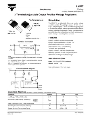
Pin Arrangement Description
The LM317 is an adjustable 3-terminal positive voltage
TO-263
regulator capable of supplying in excess of 1.5A over an
(LM317CM)
output voltage range of 1.2V to 37V. This voltage regulator
3 is exceptionally easy to use and requires only two external
2
3 1 resistors to set the output voltage. Further, it employs internal
TO-220 2 current limiting, thermal shutdown and safe area compen-
(LM317CT) 1 1. Adjust sation, making it essentially blow-out proof.
2. Vout
3. Vin
Heatsink is connected to pin 2 Features
• Output current in excess of 1.5 ampere
Standard Application
• Output adjustable between 1.2V and 37V
Vin Vout • Internal thermal overload protection
LM317
R1 • Internal short-circuit current limiting
IADJ Adjust 240Ω constant with temperature
Cin Co
0.1µF 1µF • Output transistor safe-area compensation
R2
• Floating operation for high voltage applications
• Eliminates stocking many fixed voltages
Notes:
Cin is required if regulator is located an appreciable distance from power
supply filter. Mechanical Data
Co is not needed for stability, however, it does improve transient response.
Vout = 1.25V (1 + R2 / R1) + IAdj R2 Case: TO-220 and TO-263 packages
Since IAdj is controlled to less than 100µA, the error associated with this Weight: approx. 1.35g
term is negligible in most applications
Case outlines are on the back page.
Input Functional Block Diagram
3
+
--
Voltage Protection
Reference Circuitry
Rlimit
Vadj 2
1 Output
Maximum Ratings Ratings at 25°C ambient temperature unless otherwise specified.
Parameter Symbol Value Unit
Input-Output Voltage Differential Vi-Vo 40 Vdc
Junction-to-Case Thermal Resistance TO-220 3.0
RθJC °C
TO-263 3.0
Power Dissipation, 25°C Case Temperature PD 15 W
Operating Junction Temperature Range TJ 0 to +125 °C
Storage Junction Temperature Range Tstg –65 to +150 °C
Document Number 74809 www.vishay.com
30-Oct-02 1
2. LM317
Vishay
formerly General Semiconductor
Electrical Characteristics – LM317
Vi -Vo = 5V, Io = 0.5A, TJ = Tlow to Thigh (see Note 1), Imax and Pmax per Note 2, unless otherwise noted.
Parameter Symbol Conditions Min. Typ. Max. Unit
Line Regulation (Fig. 1) (3) TA = 25°C – 0.01 0.04
REG line %Vo/V
3.0V ≤ VI – Vo ≤ 40V TJ = 0°C thru 125°C – 0.02 0.07
Load Regulation (Fig. 2) (3) Vo ≤ 5.0 – 5 25 mV
REG load
TJ = 25°C, 10mA ≤ Io ≤ 1.5A Vo ≥ 5.0 – 0.1 0.5 %Vo
Load Regulation (Fig. 2) (3) Vo ≤ 5.0 – 20 70 mV
REG load
10mA ≤ Io ≤ 1.5A Vo ≥ 5.0 – 0.3 1.5 %Vo
Thermal Regulation REG therm TJ = 25°C, 20ms Pulse – 0.03 0.07 %Vo/W
Adjustment Pin Current (Fig. 3) IAdj – 50 100 µA
10mA ≤ IL ≤ 1.5A
Adjustment Pin Current Change ∆IAdj – 0.2 5 µA
2.5V ≤ VI – Vo ≤ 40V
10mA ≤ Io ≤ 1.5A
Reference Voltage (Fig. 3) (4) Vref 1.225 1.25 1.275 V
3V ≤ VI – Vo ≤ 40V
Temperature Stability (Fig. 3) TS Tlow ≤ TJ ≤ Thigh – 1 – %Vo
Min. Load Current to Maintain Regulation (Fig. 3) ILmin VI – Vo = 40V – 3.5 10 mA
VI – Vo ≤ 15V 1.5 2.2 –
Maximum Output Current (Fig. 3) Imax A
VI – Vo = 40V, TJ = 25°C 0.15 0.4 –
RMS Noise, % of Vo N TJ = 25°C, 10HZ ≤ f ≤ 10KHZ — 0.003 – %Vo
Vo = 10V, f = 120HZ(5) — 65 –
Ripple Rejection (Fig. 4) RR dB
CAdj = 10µF 66 80 –
TJ = 125°C(6), TJ = 25°C for
Long-Term Stability (after 1000 hr) Fig. 3 S – 0.3 1.0 %
Endpoint Measurements
Thermal Resistance Junction to Case RθJC Tlow ≤ TJ ≤ Thigh – 5.0 – °C/W
Notes:
(1) Tlow = 0°C Thigh = 125°C
(2) Imax = 1.5A Pmax is internally limited
(3) Load and line regulation are specified at constant junction temperature. Changes in Vo due to heating effects must be taken into account separately.
Pulse testing with low duty cycle is used.
(4) Selected devices with tightened tolerance reference voltage available.
(5) CAdj, when used, is connected between the addjustment pin and ground.
(6) Since Long-Term Stability cannot be measured on each device before shipment, this specification is an engineering estimate of average stability from lot to lot.
www.vishay.com Document Number 74809
2 30-Oct-02
3. LM317
Vishay
formerly General Semiconductor
Fig. 1 – Line Regulation Test Circuit Fig. 2 – Load Regulation and
∆Iadj /Load Test Circuit
V V
Line Regulation (%/V) = OH -- OL x100 Load Regulator (mV) = Vo(min. Load) -- Vo(max. Load)
VOL Vo(min. Load) -- Vo(max. Load)
Load Regulator (%Vo) = x100
Vo(min. Load)
VIH VOH
VIL VOL VOH (min. Load)
Vin Vout VI Vin Vout VOL (max. Load)
LM317 LM317 IL
Adjust R1 240Ω Adjust R1 240Ω
IADJ 1% IADJ 1%
Co RL
Cin RL Cin Co (min.
0.1µF 1µF Load)
R2 0.1µF R2 1µF
1% 1%
Pulse Testing Required: Pulse Testing Required:
1% Duty Cycle is Suggested 1% Duty Cycle is Suggested
Fig. 3 – Standard Test Circuit Fig. 4 – Ripple Rejection Test Circuit
24V
14V
f = 120HZ
Vin Vout Vin Vout Vo = 10V
LM317 IL LM317
*D1
Adjust R1 240 240 1N4002
1% Vref R1 1%
IADJ Adjust
Cin Co
Cin Co
VI 0.1µF RL Vo RL Vo
1µF
ISET 0.1µF 1µF
CAdj
R2 R2 10µF
1% 1%
To Calculate R2:
Pulse Testing Required: Vo = ISET R2 + 1.250V *D1 Discharges CADJ if
1% Duty Cycle is Suggested Assume ISET = 5.25mA Output is Shorted to Ground
Document Number 74809 www.vishay.com
30-Oct-02 3
4. LM317
Vishay
formerly General Semiconductor
Ratings and
Characteristic Curves (T A = 25°C unless otherwise noted)
Fig. 5 – Load Regulation Fig. 6 – Current Limit
0.6 4
∆Vo -- Output Voltage Change (%)
0.4
0.2 3
Io -- Output Current (A)
IL = 0.5A
0 TJ = 25°C
--0.2 2
IL = 1.5A
--0.4 TJ = 150°C TJ = --55°C
VI = 15V
--0.6 1
Vo = 10V
--0.8
--1.0 0
--75 --50 --25 0 25 50 75 100 125 150 175 0 10 20 30 40
Fig. 7 – Adjustment Pin Current Fig. 8 – Dropout Voltage
75 3.0
IADJ -- Adjustment Pin Current (µA)
70
VI -- Vo -- Input -- Output Voltage
∆Vo = 100mV
65 2.5
Differential (Vdc)
IL = 1.5A
60
55 2.0 IL = 1.0A
50
IL = 500mA
45 1.5
IL = 200mA
40 IL = 20mA
35 1.0
--75 --50 --25 0 25 50 75 100 125 150 175 --75 --50 --25 0 25 50 75 100 125 150 175
Fig. 9 – Temperature Stability Fig. 10 – Minimum Operating Current
1.260 5.0
4.5
Vref -- Reference Voltage (V)
IO -- Quiescent Current (mA)
4.0
1.250 TJ = 25°C
3.5
TJ = --55°C TJ = 150°C
3.0
1.240 2.5
2.0
1.5
1.230
1.0
0.5
1.220 0
--75 --50 --25 0 25 50 75 100 125 150 175 0 10 20 30 40 50
www.vishay.com Document Number 74809
4 30-Oct-02
5. LM317
Vishay
formerly General Semiconductor
Ratings and
Characteristic Curves (T A = 25°C unless otherwise noted)
Fig. 11 – Ripple Rejection Fig. 12 – Ripple Rejection
vs. Output Voltage vs. Output Current
100 140
CAdj = 10µF
120
80
RR -- Ripple Rejection (db)
RR -- Ripple Rejection (db)
100 CAdj = 10µF
Without CAdj
60 80
60 Without CAdj
40
VI -- Vo = 5V 40 VI = 15V
20 IL = 500mA Vo = 10V
f = 120HZ 20 f = 120HZ
TJ = 25°C TJ = 25°C
0 0
0 5 10 15 20 25 30 35 40 0.01 0.1 1 10
Vo -- Output Voltage (V) Io -- Output Current (A)
Fig. 13 – Ripple Rejection
vs. Frequency Fig. 14 – Output Impedance
100 101
VI = 15V
80 Vo = 10V
RR -- Ripple Rejection (db)
100 IL = 500mA
Output Impedance (Ω)
TJ = 25°C
CAdj = 10µF
60
Without CAdj
10--1
40 Without CAdj
IL = 500mA
10--2
20 VI = 15V
CAdj = 10µF
Vo = 10V
TJ = 25°C
0 10--3
10 100 1K 10K 100K 1M 10 100 1K 10K 100K 1M
f -- Frequency (Hz) f -- Frequency (Hz)
Fig. 15 – Line Transient Response Fig. 16 – Load Transient Response
∆VI -- Input Voltage ∆Vo -- Output Voltage
3
Deviation (V)
Vo -- Output Voltage
1.5 2
Deviation (V)
1.0 1 CL = 1µF CAdj = 10µF
CL = 1µF CAdj = 10µF
0.5 0
0 --1
--0.5 Vo = 10V --2
IL = 50mA CL = 0 Without CAdj VI = 15V
--1.0 --3
TJ = 25°C Vo = 10V
Change (V)
Current (A)
INL = 50mA
IL -- Load
--1.5 CL = 0 1.5
Without CAdj TJ = 25°C
1.0 1.0
VI IL
0.5 0.5
0 0
0 10 20 30 40 0 10 20 30 40
t -- Time (µs) t -- Time (µs)
Document Number 74809 www.vishay.com
30-Oct-02 5