SlideShare uma empresa Scribd logo
1 de 18
Baixar para ler offline
M                                                                                      AN843
            Speed Control of 3-Phase Induction Motor Using
                       PIC18 Microcontrollers

 Author:    Padmaraja Yedamale                             Induction Motor Basics
            Microchip Technology Inc.
                                                           NAMEPLATE PARAMETERS
                                                           A typical nameplate of an induction motor lists the
                                                           following parameters:
INTRODUCTION
                                                           •   Rated terminal supply voltage in Volts
Induction motors are the most widely used motors for       •   Rated frequency of the supply in Hz
appliances, industrial control, and automation; hence,
                                                           •   Rated current in Amps
they are often called the workhorse of the motion indus-
try. They are robust, reliable, and durable. When power    •   Base speed in RPM
is supplied to an induction motor at the recommended       •   Power rating in Watts or Horsepower (HP)
specifications, it runs at its rated speed. However,       •   Rated torque in Newton Meters or Pound-Inches
many applications need variable speed operations. For      •   Slip speed in RPM, or slip frequency in Hz
example, a washing machine may use different speeds
                                                           •   Winding insulation type - Class A, B, F or H
for each wash cycle. Historically, mechanical gear sys-
tems were used to obtain variable speed. Recently,         •   Type of stator connection (for 3-phase only), star
electronic power and control systems have matured to           (Y) or delta (∆)
allow these components to be used for motor control in     When the rated voltage and frequency are applied to
place of mechanical gears. These electronics not only      the terminals of an induction motor, it draws the rated
control the motor’s speed, but can improve the motor’s     current (or corresponding power) and runs at base
dynamic and steady state characteristics. In addition,     speed and can deliver the rated torque.
electronics can reduce the system’s average power
consumption and noise generation of the motor.             MOTOR ROTATION
Induction motor control is complex due to its nonlinear    When the rated AC supply is applied to the stator wind-
characteristics. While there are different methods for     ings, it generates a magnetic flux of constant magni-
control, Variable Voltage Variable Frequency (VVVF) or     tude, rotating at synchronous speed. The flux passes
V/f is the most common method of speed control in          through the air gap, sweeps past the rotor surface and
open loop. This method is most suitable for applica-       through the stationary rotor conductors. An electro-
tions without position control requirements or the need    motive force (EMF) is induced in the rotor conductors
for high accuracy of speed control. Examples of these      due to the relative speed differences between the rotat-
applications include heating, air conditioning, fans and   ing flux and stationary conductors.
blowers. V/f control can be implemented by using low
                                                           The frequency of the induced EMF is the same as the
cost PICmicro microcontrollers, rather than using
                                                           supply frequency. Its magnitude is proportional to the
costly digital signal processors (DSPs).
                                                           relative velocity between the flux and the conductors.
Many PICmicro microcontrollers have two hardware           Since the rotor bars are shorted at the ends, the EMF
PWMs, one less than the three required to control a        induced produces a current in the rotor conductors.
3-phase induction motor. In this application note, we      The direction of the rotor current opposes the relative
will generate a third PWM in software, using a general     velocity between rotating flux produced by stator and
purpose timer and an I/O pin resource that are readily     stationary rotor conductors (per Lenz's law).
available on the PICmicro microcontroller. This applica-
                                                           To reduce the relative speed, the rotor starts rotating in
tion note also covers the basics of induction motors and
                                                           the same direction as that of flux and tries to catch up
different types of induction motors.
                                                           with the rotating flux. But in practice, the rotor never
  Note:    Refer to Appendix C for glossary of             succeeds in 'catching up' to the stator field. So, the
           technical terms.                                rotor runs slower than the speed of the stator field. This
                                                           difference in speed is called slip speed. This slip speed
                                                           depends upon the mechanical load on the motor shaft.


 2002 Microchip Technology Inc.                                                                   DS00843A-page 1
AN843
The frequency and speed of the motor, with respect to
the input supply, is called the synchronous frequency               Note 1: Percentage of slip varies with load on the
and synchronous speed. Synchronous speed is                                 motor shaft.
directly proportional to the ratio of supply frequency
                                                                          2: As the load increases, the slip also
and number of poles in the motor. Synchronous speed
                                                                             increases.
of an induction motor is shown in Equation 1.

EQUATION 1:                                                    INDUCTION MOTOR TYPES
        Synchronous Speed (Ns) = 120 x F/P                     Based on the construction of the rotor, induction motors
 where:                                                        are broadly classified in two categories: squirrel cage
                                                               motors and slip ring motors. The stator construction is
     F = rated frequency of the motor
                                                               the same in both motors.
     P = number of poles in the motor
                                                               Squirrel Cage Motor
                                                               Almost 90% of induction motors are squirrel cage
   Note 1: The number of poles is the number of
                                                               motors. This is because the squirrel cage motor has a
           parallel paths for current flow in the stator.
                                                               simple and rugged construction. The rotor consists of a
         2: The number of poles is always an even              cylindrical laminated core with axially placed parallel
            number to balance the current flow.                slots for carrying the conductors. Each slot carries a
         3: 4-pole motors are the most widely used             copper, aluminum, or alloy bar. If the slots are semi-
            motors.                                            closed, then these bars are inserted from the ends.
                                                               These rotor bars are permanently short-circuited at
Synchronous speed is the speed at which the stator             both ends by means of the end rings, as shown in
flux rotates. Rotor flux rotates slower than synchronous       Figure 1. This total assembly resembles the look of a
speed by the slip speed. This speed is called the base         squirrel cage, which gives the motor its name. The rotor
speed. The speed listed on the motor nameplate is the          slots are not exactly parallel to the shaft. Instead, they
base speed. Some manufacturers also provide the slip           are given a skew for two main reasons:
as a percentage of synchronous speed as shown in
Equation 2.                                                    a)    To make the motor run quietly by reducing the
                                                                     magnetic hum.
EQUATION 2:                                                    b)    To help reduce the locking tendency of the rotor.
                                                                     Rotor teeth tend to remain locked under the sta-
    Base Speed N = Synchronous Speed – Slip Speed                    tor teeth due to direct magnetic attraction
                  (Synchronous Speed – Base Speed) x 100             between the two. This happens if the number of
 Percent Slip =                                                      stator teeth are equal to the number of rotor
                           Synchronous Speed
                                                                     teeth.


FIGURE 1:            TYPICAL SQUIRREL CAGE ROTOR

                                                  Conductors            End rings

                     Shaft


                                         Bearings
                                                                Skewed Slots


DS00843A-page 2                                                                          2002 Microchip Technology Inc.
AN843
Slip Ring Motors                                                 The current drops significantly when the motor speed
                                                                 approaches ~80% of the rated speed. At base speed,
The windings on the rotor are terminated to three insu-
                                                                 the motor draws the rated current and delivers the
lated slip rings mounted on the shaft with brushes rest-
                                                                 rated torque.
ing on them. This allows an introduction of an external
resistor to the rotor winding. The external resistor can         At base speed, if the load on the motor shaft is
be used to boost the starting torque of the motor and            increased beyond its rated torque, the speed starts
change the speed-torque characteristic. When running             dropping and slip increases. When the motor is running
under normal conditions, the slip rings are short-               at approximately 80% of the synchronous speed, the
circuited, using an external metal collar, which is              load can increase up to 2.5 times the rated torque. This
pushed along the shaft to connect the rings. So, in              torque is called breakdown torque. If the load on the
normal conditions, the slip ring motor functions like a          motor is increased further, it will not be able to take any
squirrel cage motor.                                             further load and the motor will stall.
                                                                 In addition, when the load is increased beyond the
SPEED-TORQUE CHARACTERISTICS OF                                  rated load, the load current increases following the cur-
INDUCTION MOTORS                                                 rent characteristic path. Due to this higher current flow
Figure 2 shows the typical speed-torque characteris-             in the windings, inherent losses in the windings
tics of an induction motor. The X axis shows speed and           increase as well. This leads to a higher temperature in
slip. The Y axis shows the torque and current. The               the motor windings. Motor windings can withstand dif-
characteristics are drawn with rated voltage and                 ferent temperatures, based on the class of insulation
frequency supplied to the stator.                                used in the windings and cooling system used in the
                                                                 motor. Some motor manufacturers provide the data on
During start-up, the motor typically draws up to seven           overload capacity and load over duty cycle. If the motor
times the rated current. This high current is a result of        is overloaded for longer than recommended, then the
stator and rotor flux, the losses in the stator and rotor        motor may burn out.
windings, and losses in the bearings due to friction. This
high starting current overcomes these components and             As seen in the speed-torque characteristics, torque is
produces the momentum to rotate the rotor.                       highly nonlinear as the speed varies. In many applica-
                                                                 tions, the speed needs to be varied, which makes the
At start-up, the motor delivers 1.5 times the rated              torque vary. We will discuss a simple open loop method
torque of the motor. This starting torque is also called         of speed control called, Variable Voltage Variable
locked rotor torque (LRT). As the speed increases, the           Frequency (VVVF or V/f) in this application note.
current drawn by the motor reduces slightly (see
Figure 2).

FIGURE 2:          SPEED-TORQUE CHARACTERISTICS OF INDUCTION MOTORS
                                     Current
                                                                         Breakdown Torque
                                                     Torque


                 Locked Rotor Torque


     Torque                                                                                     Full Load Torque
     Current
                                                                                                          TRATED
                                                                                                          IRATED
                          Pull-up Torque


                                                                                          NB        NS
                                                        Slip Speed


 2002 Microchip Technology Inc.                                                                         DS00843A-page 3
AN843
V/f CONTROL THEORY                                              EQUATION 3:
As we can see in the speed-torque characteristics, the           Stator Voltage (V) ∝ [Stator Flux(φ)] x [Angular Velocity (ω)]
induction motor draws the rated current and delivers             V ∝ φ x 2πf
the rated torque at the base speed. When the load is             φ ∝ V/f
increased (over-rated load), while running at base
speed, the speed drops and the slip increases. As we
                                                                This makes constant V/f the most common speed
have seen in the earlier section, the motor can take up
                                                                control of an induction motor.
to 2.5 times the rated torque with around 20% drop in
the speed. Any further increase of load on the shaft can        Figure 3 shows the relation between the voltage and
stall the motor.                                                torque versus frequency. Figure 3 demonstrates volt-
                                                                age and frequency being increased up to the base
The torque developed by the motor is directly propor-
                                                                speed. At base speed, the voltage and frequency reach
tional to the magnetic field produced by the stator. So,
                                                                the rated values as listed in the nameplate. We can
the voltage applied to the stator is directly proportional
                                                                drive the motor beyond base speed by increasing the
to the product of stator flux and angular velocity. This
                                                                frequency further. However, the voltage applied cannot
makes the flux produced by the stator proportional to
                                                                be increased beyond the rated voltage. Therefore, only
the ratio of applied voltage and frequency of supply.
                                                                the frequency can be increased, which results in the
By varying the frequency, the speed of the motor can            field weakening and the torque available being
be varied. Therefore, by varying the voltage and fre-           reduced. Above base speed, the factors governing
quency by the same ratio, flux and hence, the torque            torque become complex, since friction and windage
can be kept constant throughout the speed range.                losses increase significantly at higher speeds. Hence,
                                                                the torque curve becomes nonlinear with respect to
                                                                speed or frequency.


FIGURE 3:          SPEED-TORQUE CHARACTERISTICS WITH V/f CONTROL


        Vrated                                                              Voltage
                                                                              Voltage


     Torque
      Torque
      oltage
        Voltage


          Vmin


                      fmin                                   frated(base speed)                          fmax
                                                         Frequency
                                                        Frequency


DS00843A-page 4                                                                             2002 Microchip Technology Inc.
AN843
IMPLEMENTATION                                             time, a maximum of three switches will be on, either
                                                           one upper and two lower switches, or two upper and
Power                                                      one lower switch.
                                                           When the switches are on, current flows from the DC
Standard AC supply is converted to a DC voltage by
                                                           bus to the motor winding. Because the motor windings
using a 3-phase diode bridge rectifier. A capacitor fil-
                                                           are highly inductive in nature, they hold electric energy
ters the ripple in the DC bus. This DC bus is used to
                                                           in the form of current. This current needs to be dissi-
generate a variable voltage and variable frequency
                                                           pated while switches are off. Diodes connected across
power supply. A voltage source power inverter is used
                                                           the switches give a path for the current to dissipate
to convert the DC bus to the required AC voltage and
                                                           when the switches are off. These diodes are also called
frequency. In summary, the power section consists of a
                                                           freewheeling diodes.
power rectifier, filter capacitor, and power inverter.
                                                           Upper and lower switches of the same limb should not
The motor is connected to the inverter as shown in
                                                           be switched on at the same time. This will prevent the
Figure 4. The power inverter has 6 switches that are
                                                           DC bus supply from being shorted. A dead time is given
controlled in order to generate an AC output from the
                                                           between switching off the upper switch and switching
DC input. PWM signals generated from the micro-
                                                           on the lower switch and vice versa. This ensures that
controller control these 6 switches. The phase voltage
                                                           both switches are not conductive when they change
is determined by the duty cycle of the PWM signals. In
                                                           states from on to off, or vice versa.

FIGURE 4:         3-PHASE INVERTER BRIDGE


     DC+
              PWM1                             PWM2                        PWM3


                                                                                                     Motor

              PWM4                             PWM5                        PWM6


      DC-


 2002 Microchip Technology Inc.                                                                  DS00843A-page 5
AN843
Control                                                       The ISR has a fixed entry latency of 3 instruction
                                                              cycles. If the interrupt is due to the Timer2 to PR2
To derive a varying AC voltage from the power inverter,       match then it takes 3 instruction cycles to check the flag
pulse width modulation (PWM) is required to control the       and branch to the code section where the Timer2 to
duration of the switches’ ON and OFF times. Three             PR2 match task is present. Therefore, this makes a
PWMs are required to control the upper three switches         minimum of six instruction cycles delay, or phase shift
of the power inverter. The lower switches are controlled      between the hardware PWM and software PWM, as
by the inverted PWM signals of the corresponding              shown in Figure 5.
upper switch. A dead time is given between switching
off the upper switch and switching on the lower switch        The falling edge of software PWM trails the hardware
and vice versa, to avoid shorting the DC bus.                 PWM by 8 instruction cycles. In the ISR, the TMR2 to
                                                              PR2 match has a higher priority than the Timer1 over-
PIC18XXX2 has two 10-bit PWMs implemented in the              flow interrupt. Thus, the control checks for TMR2 to
hardware. The PWM frequency can be set using the              PR2 match interrupt first. This adds 2 instruction cycles
PR2 register. This frequency is common for both               when the interrupt is caused by Timer1 overflow, mak-
PWMs. The upper eight bits of duty cycle are set using        ing a total delay of 8 instruction cycles. Figure 5 shows
the register CCPRxL. The lower two bits are set in            the hardware PWM and PWM generated by software
CCPxCON<5:4>. The third PWM is generated in the               for the same duty cycle.
software and output to a port pin.
                                                              A sine table is created in the program memory, which is
SOFTWARE PWM IMPLEMENTATION                                   transferred to the data memory upon initialization.
                                                              Three registers are used as the offset to the table. Each
Timer2 is an 8-bit timer used to control the timing of        of these registers will point to one of the values in the
hardware PWMs. The main processor is interrupted              table, such that they will have a 120 degrees phase
when the Timer2 value matches the PR2 value, if a cor-        shift to each other as shown in the Figure 6. This forms
responding interrupt enable bit is set.                       three sine waves, with 120 degrees phase shift to each
Timer1 is used for setting the duty cycle of the software     other.
PWM (PWM3). In the Timer2 to PR2 match Interrupt              After every Timer0 overflow interrupt, the value pointed
Service Routine (ISR), the port pin designated for            to by the offset registers on the sine table is read. The
PWM3 is set to high. Also, the Timer1 is loaded with the      value read from the table is scaled based on the motor
value which corresponds to the PWM3 duty cycle. In            frequency input, by multiplying by the frequency input
Timer1 overflow interrupt, the port pin designated for        value to find the ratio of PWM, with respect to the max-
PWM3 is cleared. As a result, the software and                imum DC bus. This value is loaded to the correspond-
hardware PWMs have the same frequency.                        ing PWM duty cycle registers. Subsequently, the offset
The software PWM will lag by a fixed delay compared           registers are updated for next access. If the direction
to the hardware PWMs. To minimize the phase lag, the          key is set to the motor to reverse rotation, then PWM1
Timer2 to PR2 match interrupt should be given highest         and PWM2 duty cycle values are loaded to PWM2 and
priority while checking for the interrupt flags in the ISR.   PWM1 duty cycle registers, respectively. Typical code
                                                              section of accessing and scaling of the PWM duty cycle
                                                              is as shown in Example 1.

FIGURE 5:          TIMING DIAGRAM OF HARDWARE AND SOFTWARE PWMS

     TMR2 to PR2 Match         Timer1 Overflow


    Hardware PWM


    Software PWM

     6 Cycles Delay
                                   8 Cycles Delay


DS00843A-page 6                                                                         2002 Microchip Technology Inc.
AN843
FIGURE 6:         REALIZATION OF 3-PHASE SINE WAVEFORM FROM A SINE TABLE


                                   Sine table+offset1

                                              Sine table+offset2
                                                         Sine table+offset3
                                                                                DC+


                                                                                DC-


 2002 Microchip Technology Inc.                                              DS00843A-page 7
AN843
EXAMPLE 1:        SINE TABLE UPDATE
 ;**********************************************************************************************
 ;This routine updates the PWM duty cycle value according to the offset to the table by
 ;0-120-240 degrees.
 ;This routine scales the PWM value from the table based on the frequency to keep V/F constant.
 ;**********************************************************************************************
     lfsr    FSR0,(SINE_TABLE) ;Initialization of FSR0 to point the starting location of
                                ;Sine table
 ;----------------------------------------------------------------------------------------------
 UPDATE_PWM_DUTYCYCLES
     movf    TABLE_OFFSET1,W    ;Offset1 value is loaded to WREG
     movf    PLUSW0,W           ;Read the value from the table start location + offset1
     bz      PWM1_IS_0
     mulwf   FREQUENCY          ;Table value X Frequency to scale the table value
     movff   PRODH,CCPR1L_TEMP ;based on the frequency
     bra     UPDATE_PWM2
 PWM1_IS_0
     clrf    CCPR1L_TEMP        ;Clear the PWM1 duty cycle register
 ;----------------------------------------------------------------------------------------------
 UPDATE_PWM2
     movf    TABLE_OFFSET2,W    ;Offset2 value is loaded to WREG
     movf    PLUSW0,W           ;Read the value from the table start location + offset2
     bz      PWM2_IS_0          ;
     mulwf   FREQUENCY          ; Table value X Frequency to scale the table value
     movff   PRODH,CCPR2L_TEMP ;based on the frequency
     bra     UPDATE_PWM3
 PWM2_IS_0
     clrf    CCPR2L_TEMP        ;Clear the PWM2 duty cycle register
 ;----------------------------------------------------------------------------------------------
 UPDATE_PWM3
     movf    TABLE_OFFSET3,W    ;Offset2 value is loaded to WREG
     movf    PLUSW0,W           ;Read the value from the table start location + offset3
     bz      PWM3_IS_0
     mulwf   FREQUENCY          ;Table value X Frequency to scale the table value
     comf    PRODH,PWM3_DUTYCYCLE;based on the frequency
     bra     SET_PWM12
 PWM3_IS_0
     clrf    PWM3_DUTYCYCLE     ;Clear the PWM3 duty cycle register
 ;---------------------------------------------------------------------------------------------
 SET_PWM12
     btfss   FLAGS,MOTOR_DIRECTION ;Is the motor direction = Reverse?
     bra     ROTATE_REVERSE         ;Yes
     movff   CCPR1L_TEMP,CCPR1L     ;No, Forward
     movff   CCPR2L_TEMP,CCPR2L     ;Load PWM1 & PWM2 to duty cycle registers
     bsf     PORT_LED1,LED1         ;LED1-ON indicating motor running forward
     return
 ;----------------------------------------------------------------------------------------------
 ROTATE_REVERSE                 ;Motor direction reverse
     movff   CCPR2L_TEMP,CCPR1L ;Load PWM1 & PWM2 to duty cycle registers
     movff   CCPR1L_TEMP,CCPR2L
     bcf PORT_LED1,LED1;LED1-OFF indicating motor running reverse
     return
 ;----------------------------------------------------------------------------------------------


DS00843A-page 8                                                         2002 Microchip Technology Inc.
AN843
The three PWMs are connected to the driver chip                 quency, and the number of sine table entries. New
(IR21362). These three PWMs switch the upper three              PWM duty cycles are loaded to the corresponding duty
switches of the power inverter. The lower switches are          cycle registers during the Timer0 overflow Interrupt
controlled by the inverted PWM signals of the corre-            Service Routine. So, the duty cycle will remain the
sponding upper switch. The driver chip generates                same until the next Timer0 overflow interrupt occurs, as
200 ns of dead time between upper and lower switches            shown in Figure 7.
of all phases.
A potentiometer connected to a 10-bit ADC channel on            EQUATION 4:
the PICmicro microcontroller determines the motor                 Timer0 Reload Value =
speed. The microcontroller uses the ADC results to cal-
culate the duty cycle of the PWMs and thus, the motor                                          FOSC 
frequency. The ADC is checked every 2.2 milliseconds,                                          4 
                                                                 FFFFh –
which provides smooth frequency transitions. Timer0 is                     Sine samples per cycle x Timer0 Prescaler x ADC
used for the timing of the motor frequency. The Timer0
period is based on the ADC result, the main crystal fre-


FIGURE 7:         TIMER0 OVERFLOW AND PWM

                          Timer2 to PR2 match Interrupt                 Timer1 overflow Interrupt
                                                    Timer0 overflow Interrupt


                                                                                                 Average voltage


        Volts
        Volts


                                                     Time
                                                    Time


 2002 Microchip Technology Inc.                                                                         DS00843A-page 9
AN843
System Overview                                                         time between the respective higher and lower PWMs.
                                                                        This driver needs an enable signal, which is controlled
Figure 8 shows an overall block diagram of the power                    by the microcontroller. The IGBT driver has two FAULT
and control circuit. A potentiometer is connected to AD                 monitoring circuits, one for over current and the second
Channel 0. The PICmicro microcontroller reads this                      for under voltage. Upon any of these FAULTS, the out-
input periodically to get the new speed or frequency ref-               puts are driven low and the FAULT pin shows that a
erence. Based on this AD result, the firmware deter-                    FAULT has occurred. If the FAULT is due to the over
mines the scaling factor for the PWM duty cycle. The                    current, it can be automatically reset after a fixed time
Timer0 reload value is calculated based on this input to                delay, based on the resistor and capacitor time
determine the motor frequency. PWM1 and PWM2 are                        constant connected to the RCIN pin of the driver.
the hardware PWMs (CCP1 and CCP2). PWM3 is the
PWM generated by software. The output of these three                    The main 3-phase supply is rectified by using the
PWMs are given to the higher and lower input pins of                    3-phase diode bridge rectifier. The DC ripple is filtered
the IGBT driver as shown in Figure 8. The IGBT driver                   by using an electrolytic capacitor. This DC bus is
has inverters on the lower input pins and adds dead-                    connected to the IGBTs for inverting it to a V/f supply.


FIGURE 8:          BLOCK DIAGRAM OF 3-PHASE INDUCTION MOTOR CONTROL


                                                3-Phase AC
                                                   Input
                                                                                    3-Phase Diode
                                                                                    Bridge Rectifier

                                                                                                    Capacitor

                                  PWM1            HIN1         HOut1           IGBTH1
  Potentiometer          ADC      PWM2            HIN2
                                  PWM3            HIN3         HOut2           IGBTH2
                                                  LIN1         HOut3           IGBTH3                           3-Phase Induction
   Fwd/Rev                                        LIN2
                           PIC18XXX                                                                                  Motor
                                                  LIN3         LOut1           IGBTL1
                                                         IGBT
   Run/Stop                           En          En     Driver LOut2          IGBTL2    3-Phase
                                                                                         Inverter
                                  FAULT           FAULT        LOut3           IGBTL3


CONCLUSION                                                              TABLE 1:          MEMORY REQUIREMENTS
To control the speed of a 3-phase induction motor in                             Memory                            Bytes
open loop, supply voltage and frequency need to be                      Program                        0.9 Kbytes
varied with constant ratio to each other. A low cost solu-
                                                                        Data                           36 bytes
tion of this control can be implemented in a PICmicro
microcontroller. This requires three PWMs to control a
3-phase inverter bridge. Many PICmicro micro-
controllers have two hardware PWMs. The third PWM
is generated in software and output to a port pin.


DS00843A-page 10                                                                                  2002 Microchip Technology Inc.
AN843
APPENDIX A:             TEST RESULTS

TABLE A-1:         TEST RESULTS

    Test #    Set Frequency (Hz)         Set Speed (RPM)         Actual Speed (RPM)   Speed Regulation (%)
      1               7.75                      223                         208              -1.875
      2               10.5                      302                         286              -0.89
      3               13.25                     381                         375              -0.33
      4               16.75                     482                         490              +0.44
      5               19.0                      546                         548              +0.11
      6               20.75                     597                         590              +0.39
      7               24.0                      690                         668              -1.22
      8               27.0                      776                         743              -1.83
      9               29.0                      834                         834               0.0
     10               33.0                      949                         922               -1.5
     11               38.0                     1092                         1078              0.78
     12               45.75                    1315                         1307             -0.44
     13               55.5                     1596                         1579             -0.94
     14               58.25                    1675                         1644             -1.72
     15                60                      1725                         1712             -0.72


Above tests are conducted on the motor with the following specifications:
•   Terminal voltage: 208-220 Volts
•   Frequency: 60 Hz
•   Horsepower: ½ HP
•   Speed: 1725 RPM
•   Current: 2.0 Amps
•   Frame: 56 NEMA


 2002 Microchip Technology Inc.                                                            DS00843A-page 11
U1                                                                  U2
                                                                                                                                                                                                                             FIGURE B-1:

                                                                                                                11                               10                          VDD       20
                                                        +5V                                                        VDD                    RE2                                               VDD
                                                                                                                                                                                                                                                                              AN843


   DS00843A-page 12
                                                                                                        VDD     32                               9                                                                21
                                                                                                                   VDD                    RE1                                                               RB0
                                                                                                                                                                                                                                                   APPENDIX B:


                                                                                                                                                 8                                      1                         22
                                                                                                                                          RE0                                MCLR           MCLR            RB1
                                                                                                                1                                30                                                               23
                                                                                                    MCLR             MCLR                 RD7                                                               RB2
                                                          R3                                                                                     29                                     2                         24
                                                                                                                                          RD6                                AN0            RA0             RB3         EN
                                                          4.7K                                                   2                               28                                     3                         25
                                               S1                                                       AN0          RA0                  RD5                                               RA1             RB4      FAULT
                                                                      D5                                         3                               27                                     4                         26
                                          1         4                                                                RA1                  RD4                                LED1           RA2             RB5        RB5
                                                                                  MCLR                           4                               22                                     5
                                          2         3                                                   LED1         RA2                  RD3                                LED2           RA3             RB6   27   RB6
                                                                    1N914                                        5                                                                      6
                                                                                                        LED2         RA3                  RD2                                S2             RA4             RB7   28   RB7
                                                              C14                                                6                               20                                     7   RA5
                                                                                                        S2           RA4                  RD1                                S1
                                                          0.1 µF                                                 7                               19                                                               11
                                                                                                        S1           RA5                  RD0                                                               RC0
                                                                                                                33   RB0                         26      RXD                                                RC1   12   RC1
                                                                                                                                          RC7
                                                                                                                34   RB1                         25                                                         RC2   13
                                                                                                                                          RC6            TXD                                                           RC2
                                                                                                                35                               24                          OSC1
                                                                                                                                                                                        9 OSC1
                                                                                                                                                                                                            RC3   14
                                                                                                                     RB2                  RC5                                                                          RC3
                                                                                                                                                                                                                             CONTROL AND DISPLAY


                                                                                                        EN      36                               23                                                         RC4   15
                                                                                                                     RB3                  RC4
                                                                                                                37   RB4                  RC3    18      RC3                                                      16
                                                                                                        FAULT                                                                                               RC5
                                       VDD              VDD          FAULT                                      38                               17                                                               17
                                                                                                        RB5          RB5                  RC2            RC2                 OSC2
                                                                                                                                                                                       10 OSC2
                                                                                                                                                                                                            RC6        TXD
                                                                                                                39                               16                                                               18
                                    C10             C11             C22                                 RB6          RB6                  RC1            RC1                                                RC7        RXD
                                                                                                                40                               15                                     8
                                                                                                        RB7          RB7                  RC0                                             VSS
                                   0.1 µF       0.1 µF          0.1 µF                                                                                                                 19 VSS
                                                                                                                                                                             VSS
                                                                                                                                         OSC2 14         OSC2
                                                                                                                                                                                              PIC16C73
                                    U1-12,12        U1-32,31          U2-7                                                                       13
                                                                                                                     VSS                 OSC1            OSC1
                                                                                                                                                                                                                                                   MOTOR CONTROL SCHEMATICS


                                                                                                        VSS          VSS

                                                                                                                           PIC18F452
                                              +5V
                                                                                                                                                                                      R5          D1
                                                                                                                                                                               LED1
                                                                                                                                                                                      470
                                          R8    4.7K                                 R9   4.7K
                                                                                                                                                                                      R6          D2
                                                                                                                                                                               LED2
                                                                                                                                                  OSC2                                470
                                                                             S1                                 S2                       Y1
                                                                                                                                                  OSC1           CW
                                                     S2                                      S3
                                                                                                                                        20 MHz              R2
                                                                                                                                                                       AN0
                                                                                                                           C12                    C13       5K
                                                          R1        4.7K                          R10    10K
                                                                                                                                                                 CCW
                                                                                                                           15 pF                 15 pF


 2002 Microchip Technology Inc.
FIGURE B-2:


 2002 Microchip Technology Inc.
                                     +20V
                                                                                                                                        POWER SUPPLY


                                    R7   10K    Optional
                                                                                        VR2

                                                CN5                                   LM340T-5.0              +5V
                                                      1                      1                                                 Jumper
                                                                                 IN           OUT 3                      VDD
                                                      2
                                   R22   6.8K                                           COM
                                                                                         2                          D6
                                                             C24      C23                           C25
                                                           100 µF   0.1 µF                         0.1 µF
                                                                                                            R40   470


                                                                                                                         VSS
                                                                                                                                                       AN843


   DS00843A-page 13
FIGURE B-3:


                                                                                  +20V
                                                                                                                                                                                                                                                            AN843


   DS00843A-page 14
                                                                             U3      1
                                                                                                                      C20   C19
                                                                                   VCC
                                                            J1                                                                                                         U6
                                    RC2                 1        2     2                                                                                          1
                                                                           HIN1                                                     K A                                                   R23 R24 R25
                                    RC1                 3        4     3   HIN2                                                                                   2
                                                        5        6     4                                                            D12 R11                       3
                                    RC3                                    HIN3                        HO1 27
                                                        7        8     5                                                                                          4
                                                                           LIN1                        LO1 16                       K A
                                                        9        10    6                                                                                          5
                                                                           LIN2                                                     D11 R12
                                            +20V       11        12    7                               HO2 23                                                     6
                                                                           LIN3                                                                                                           C27   C28 C29
                                                                                                                                                                  7
                                                                                                                                                                                                                                            POWER SECTION


                                                                                                                                                                                                                        CN1
                                                                                                       LO2 15                       K A                           8                                                    1
                                                                                                           19                       D10 R13                       9
                                                 R20                                                   HO3                                                                                                             2
                                                                                                                                                                 10                                                    3
                                                                                                       LO3 14                       K A                          11
                                                                      11                                                             D9 R14


                                                                                       IR21362_DIP28
                                                                           RCIN                                                                                  12
                                                                       8   FAULT                       COM 13                                                    13


                                                                                                                                                                           CPV364M4U
                                                                      10                                                                                                                                                 M1
                                                 C21                       EN                                                       K A                          14
                                                                       9                               VSS 12                                                                             R27   R28 R29                  M2
                                                                           ITRIP                                                     D8 R15                      15                                                      M3
                                                                      28   VB1                                                                                   16
                                                                                                                                    K A                                                                                 CN2
                                                                                                                                                                 17                                                    1
                                                                                                                                     D4 R16                      18                                                        DC+
                                                                                                                                                                                                                       2


                                                                            VB3
                                                                            VS3


                                                                            VS1
                                                                            VB2
                                                                            VS2
                                                                                                                                                                 19                       C30   C31 C32
                                                                                                                                                                                                                       3    DC-


                                                                           20
                                                                           18


                                                                           26
                                                                           24
                                                                           22
                                                                                                                                                                                            U5
                                                                                                                                           C15
                                             +5V
                                                                                                                                                                      P1
                                                                                                                                                                      P2


                                                                                                                                         R17               CN3
                                                                                                        C18                                                                                        P5                                 CN4
                                                                                                                                                         AC1     1                                                  470 R41       1
                                                                                                                                        1Ω, 2W
                                           R21                                                                                                           AC2     2                                                                2
                                                                                                                                  R18            R19             3                                        C8   C9
                                                                          C16           C17                                 M3                           AC3                                                                      3
                                                                                                                                                                                                   P4
                                                                                                                            M2                                                                                          D7
                                   FAULT                                                                                                                         P6    P3
                                                                                                                            M1
                                   EN                                              K                      K                                                             +20V
                                                                      K D13                  D14                D15
                                                                      A            A                      A                                    CN6
                                                                                                                                                     1
                                                       C26                                                                                           2
                                                                                                                                                          C7          C1
                                                                                  +20V
                                                                                                                                                                                   AGND


 2002 Microchip Technology Inc.
AN843
APPENDIX C:            GLOSSARY                           Locked Rotor Torque
                                                          Starting torque of the motor.
Air Gap
Uniform gap between the stator and rotor.                 Pull-up Torque
                                                          Torque available on the rotor at around 20% of base
Angular Velocity                                          speed.
Velocity in radians (2π x frequency).
                                                          Rotor
Asynchronous Motor                                        Rotating part of the motor.
Type of motor in which the flux generated by the stator
and rotor have different frequencies.                     Slip Speed
                                                          Synchronous speed minus base speed.
Base Speed
Speed specified on the nameplate of an induction          Stator
motor.                                                    Stationary part of the motor.

Break Down Torque                                         Synchronous Motor
Maximum torque on the speed-torque characteristics        Type of motor in which the flux generated by the stator
at approximately 80% of base speed.                       and rotor have the same frequencies. The phase may
                                                          be shifted.
EMF
Electromotive Force. The potential generated by a cur-    Synchronous Speed
rent carrying conductor when it is exposed to magnetic    Speed of the motor corresponding to the rated
field. EMF is measured in volts.                          frequency.

Full Load Torque                                          Torque
Rated torque of the motor as specified on the             Rotating force in Newton-Meters or Pound-Inches.
nameplate.

IGBT
Insulated Gate Bipolar Transistor.

Lenz’s Law
The Electromotive force (EMF) induced in a conductor
moving perpendicular to a magnetic field tends to
oppose that motion.


 2002 Microchip Technology Inc.                                                              DS00843A-page 15
AN843
APPENDIX D:             SOFTWARE
                        DISCUSSED IN THIS
                        TECHNICAL BRIEF
Because of its overall length, a complete source file list-
ing is not provided. The complete source code is avail-
able as a single WinZip archive file, which may be
downloaded from the Microchip corporate web site at:


                 www.microchip.com


DS00843A-page 16                                               2002 Microchip Technology Inc.
Note the following details of the code protection feature on PICmicro® MCUs.

•    The PICmicro family meets the specifications contained in the Microchip Data Sheet.
•    Microchip believes that its family of PICmicro microcontrollers is one of the most secure products of its kind on the market today,
     when used in the intended manner and under normal conditions.
•    There are dishonest and possibly illegal methods used to breach the code protection feature. All of these methods, to our knowl-
     edge, require using the PICmicro microcontroller in a manner outside the operating specifications contained in the data sheet.
     The person doing so may be engaged in theft of intellectual property.
•    Microchip is willing to work with the customer who is concerned about the integrity of their code.
•    Neither Microchip nor any other semiconductor manufacturer can guarantee the security of their code. Code protection does not
     mean that we are guaranteeing the product as “unbreakable”.
•    Code protection is constantly evolving. We at Microchip are committed to continuously improving the code protection features of
     our product.
If you have any further questions about this matter, please contact the local sales office nearest to you.


Information contained in this publication regarding device               Trademarks
applications and the like is intended through suggestion only
and may be superseded by updates. It is your responsibility to           The Microchip name and logo, the Microchip logo, FilterLab,
ensure that your application meets with your specifications.             KEELOQ, microID, MPLAB, PIC, PICmicro, PICMASTER,
No representation or warranty is given and no liability is               PICSTART, PRO MATE, SEEVAL and The Embedded Control
assumed by Microchip Technology Incorporated with respect                Solutions Company are registered trademarks of Microchip Tech-
to the accuracy or use of such information, or infringement of           nology Incorporated in the U.S.A. and other countries.
patents or other intellectual property rights arising from such
                                                                         dsPIC, ECONOMONITOR, FanSense, FlexROM, fuzzyLAB,
use or otherwise. Use of Microchip’s products as critical com-
                                                                         In-Circuit Serial Programming, ICSP, ICEPIC, microPort,
ponents in life support systems is not authorized except with
                                                                         Migratable Memory, MPASM, MPLIB, MPLINK, MPSIM,
express written approval by Microchip. No licenses are con-
                                                                         MXDEV, MXLAB, PICC, PICDEM, PICDEM.net, rfPIC, Select
veyed, implicitly or otherwise, under any intellectual property
                                                                         Mode and Total Endurance are trademarks of Microchip
rights.
                                                                         Technology Incorporated in the U.S.A.

                                                                         Serialized Quick Turn Programming (SQTP) is a service mark
                                                                         of Microchip Technology Incorporated in the U.S.A.

                                                                         All other trademarks mentioned herein are property of their
                                                                         respective companies.

                                                                         © 2002, Microchip Technology Incorporated, Printed in the
                                                                         U.S.A., All Rights Reserved.

                                                                              Printed on recycled paper.


                                                                        Microchip received QS-9000 quality system
                                                                        certification for its worldwide headquarters,
                                                                        design and wafer fabrication facilities in
                                                                        Chandler and Tempe, Arizona in July 1999
                                                                        and Mountain View, California in March 2002.
                                                                        The Company’s quality system processes and
                                                                        procedures are QS-9000 compliant for its
                                                                        PICmicro® 8-bit MCUs, KEELOQ® code hopping
                                                                        devices, Serial EEPROMs, microperipherals,
                                                                        non-volatile memory and analog products. In
                                                                        addition, Microchip’s quality system for the
                                                                        design and manufacture of development
                                                                        systems is ISO 9001 certified.


 2002 Microchip Technology Inc.                                                                                        DS00843A - page 17
M
                               WORLDWIDE SALES AND SERVICE
AMERICAS                                ASIA/PACIFIC                                 Japan
                                                                                     Microchip Technology Japan K.K.
Corporate Office                        Australia
                                                                                     Benex S-1 6F
2355 West Chandler Blvd.                Microchip Technology Australia Pty Ltd
                                                                                     3-18-20, Shinyokohama
Chandler, AZ 85224-6199                 Suite 22, 41 Rawson Street
                                                                                     Kohoku-Ku, Yokohama-shi
Tel: 480-792-7200 Fax: 480-792-7277     Epping 2121, NSW
                                                                                     Kanagawa, 222-0033, Japan
Technical Support: 480-792-7627         Australia
                                                                                     Tel: 81-45-471- 6166 Fax: 81-45-471-6122
Web Address: http://www.microchip.com   Tel: 61-2-9868-6733 Fax: 61-2-9868-6755
                                                                                     Korea
Rocky Mountain                          China - Beijing
                                                                                     Microchip Technology Korea
2355 West Chandler Blvd.                Microchip Technology Consulting (Shanghai)
                                                                                     168-1, Youngbo Bldg. 3 Floor
Chandler, AZ 85224-6199                 Co., Ltd., Beijing Liaison Office
                                                                                     Samsung-Dong, Kangnam-Ku
Tel: 480-792-7966 Fax: 480-792-4338     Unit 915
                                                                                     Seoul, Korea 135-882
                                        Bei Hai Wan Tai Bldg.
Atlanta                                 No. 6 Chaoyangmen Beidajie
                                                                                     Tel: 82-2-554-7200 Fax: 82-2-558-5934
500 Sugar Mill Road, Suite 200B         Beijing, 100027, No. China                   Singapore
Atlanta, GA 30350                       Tel: 86-10-85282100 Fax: 86-10-85282104      Microchip Technology Singapore Pte Ltd.
Tel: 770-640-0034 Fax: 770-640-0307                                                  200 Middle Road
                                        China - Chengdu
Boston                                                                               #07-02 Prime Centre
                                        Microchip Technology Consulting (Shanghai)   Singapore, 188980
2 Lan Drive, Suite 120
                                        Co., Ltd., Chengdu Liaison Office            Tel: 65-6334-8870 Fax: 65-6334-8850
Westford, MA 01886
                                        Rm. 2401, 24th Floor,
Tel: 978-692-3848 Fax: 978-692-3821
                                        Ming Xing Financial Tower                    Taiwan
Chicago                                 No. 88 TIDU Street                           Microchip Technology (Barbados) Inc.,
333 Pierce Road, Suite 180              Chengdu 610016, China                        Taiwan Branch
Itasca, IL 60143                        Tel: 86-28-86766200 Fax: 86-28-86766599      11F-3, No. 207
Tel: 630-285-0071 Fax: 630-285-0075                                                  Tung Hua North Road
                                        China - Fuzhou                               Taipei, 105, Taiwan
Dallas                                  Microchip Technology Consulting (Shanghai)
4570 Westgrove Drive, Suite 160                                                      Tel: 886-2-2717-7175 Fax: 886-2-2545-0139
                                        Co., Ltd., Fuzhou Liaison Office
Addison, TX 75001                       Unit 28F, World Trade Plaza
Tel: 972-818-7423 Fax: 972-818-2924     No. 71 Wusi Road
Detroit
                                                                                     EUROPE
                                        Fuzhou 350001, China
Tri-Atria Office Building               Tel: 86-591-7503506 Fax: 86-591-7503521      Austria
32255 Northwestern Highway, Suite 190                                                Microchip Technology Austria GmbH
                                        China - Shanghai
Farmington Hills, MI 48334                                                           Durisolstrasse 2
                                        Microchip Technology Consulting (Shanghai)
Tel: 248-538-2250 Fax: 248-538-2260                                                  A-4600 Wels
                                        Co., Ltd.
Kokomo                                                                               Austria
                                        Room 701, Bldg. B
2767 S. Albright Road                                                                Tel: 43-7242-2244-399
                                        Far East International Plaza
Kokomo, Indiana 46902                                                                Fax: 43-7242-2244-393
                                        No. 317 Xian Xia Road
Tel: 765-864-8360 Fax: 765-864-8387     Shanghai, 200051                             Denmark
Los Angeles                             Tel: 86-21-6275-5700 Fax: 86-21-6275-5060    Microchip Technology Nordic ApS
                                                                                     Regus Business Centre
18201 Von Karman, Suite 1090            China - Shenzhen
Irvine, CA 92612                                                                     Lautrup hoj 1-3
                                        Microchip Technology Consulting (Shanghai)   Ballerup DK-2750 Denmark
Tel: 949-263-1888 Fax: 949-263-1338     Co., Ltd., Shenzhen Liaison Office           Tel: 45 4420 9895 Fax: 45 4420 9910
New York                                Rm. 1315, 13/F, Shenzhen Kerry Centre,
150 Motor Parkway, Suite 202            Renminnan Lu                                 France
Hauppauge, NY 11788                     Shenzhen 518001, China                       Microchip Technology SARL
Tel: 631-273-5305 Fax: 631-273-5335     Tel: 86-755-2350361 Fax: 86-755-2366086      Parc d’Activite du Moulin de Massy
                                                                                     43 Rue du Saule Trapu
San Jose                                China - Hong Kong SAR                        Batiment A - ler Etage
Microchip Technology Inc.               Microchip Technology Hongkong Ltd.           91300 Massy, France
2107 North First Street, Suite 590      Unit 901-6, Tower 2, Metroplaza              Tel: 33-1-69-53-63-20 Fax: 33-1-69-30-90-79
San Jose, CA 95131                      223 Hing Fong Road
Tel: 408-436-7950 Fax: 408-436-7955                                                  Germany
                                        Kwai Fong, N.T., Hong Kong
                                                                                     Microchip Technology GmbH
Toronto                                 Tel: 852-2401-1200 Fax: 852-2401-3431
                                                                                     Gustav-Heinemann Ring 125
6285 Northam Drive, Suite 108           India                                        D-81739 Munich, Germany
Mississauga, Ontario L4V 1X5, Canada    Microchip Technology Inc.                    Tel: 49-89-627-144 0 Fax: 49-89-627-144-44
Tel: 905-673-0699 Fax: 905-673-6509     India Liaison Office
                                                                                     Italy
                                        Divyasree Chambers
                                                                                     Microchip Technology SRL
                                        1 Floor, Wing A (A3/A4)
                                                                                     Centro Direzionale Colleoni
                                        No. 11, O’Shaugnessey Road
                                                                                     Palazzo Taurus 1 V. Le Colleoni 1
                                        Bangalore, 560 025, India
                                                                                     20041 Agrate Brianza
                                        Tel: 91-80-2290061 Fax: 91-80-2290062
                                                                                     Milan, Italy
                                                                                     Tel: 39-039-65791-1 Fax: 39-039-6899883
                                                                                     United Kingdom
                                                                                     Microchip Ltd.
                                                                                     505 Eskdale Road
                                                                                     Winnersh Triangle
                                                                                     Wokingham
                                                                                     Berkshire, England RG41 5TU
                                                                                     Tel: 44 118 921 5869 Fax: 44-118 921-5820

                                                                                                                           05/16/02


DS00843A-page 18                                                                              2002 Microchip Technology Inc.

Mais conteúdo relacionado

Mais procurados

Necessity of starter in induction motor
Necessity of starter in induction motorNecessity of starter in induction motor
Necessity of starter in induction motorjohny renoald
 
Excitation Synchronous Wind Power Generators With Maximum Power Tracking Scheme
Excitation Synchronous Wind Power Generators With Maximum Power Tracking SchemeExcitation Synchronous Wind Power Generators With Maximum Power Tracking Scheme
Excitation Synchronous Wind Power Generators With Maximum Power Tracking SchemeProjectsatbangalore
 
Chapter 4 synchronous machine
Chapter 4 synchronous machineChapter 4 synchronous machine
Chapter 4 synchronous machinemkazree
 
Induction Synchronous Motor
Induction Synchronous MotorInduction Synchronous Motor
Induction Synchronous MotorShahzad Khalil
 
Synchronous generators
Synchronous generatorsSynchronous generators
Synchronous generatorstes4
 
POWER SYSTEM ANALYSIS-3
POWER SYSTEM ANALYSIS-3POWER SYSTEM ANALYSIS-3
POWER SYSTEM ANALYSIS-3M Ugur Kebir
 
Chapter 3 induction machine
Chapter 3 induction machineChapter 3 induction machine
Chapter 3 induction machinemkazree
 
Static excitation-system
Static excitation-systemStatic excitation-system
Static excitation-systemDeepak Jha
 
Rotating Electrical Machines-AC & DC Machines,Induction Motor and DC Motor
Rotating Electrical Machines-AC & DC Machines,Induction Motor and DC MotorRotating Electrical Machines-AC & DC Machines,Induction Motor and DC Motor
Rotating Electrical Machines-AC & DC Machines,Induction Motor and DC MotorPrasant Kumar
 
Alternating Current Machines 1a
Alternating Current Machines 1aAlternating Current Machines 1a
Alternating Current Machines 1aTalia Carbis
 
Single phase induction motor
Single phase induction motorSingle phase induction motor
Single phase induction motorSirat Mahmood
 

Mais procurados (20)

Necessity of starter in induction motor
Necessity of starter in induction motorNecessity of starter in induction motor
Necessity of starter in induction motor
 
Excitation Synchronous Wind Power Generators With Maximum Power Tracking Scheme
Excitation Synchronous Wind Power Generators With Maximum Power Tracking SchemeExcitation Synchronous Wind Power Generators With Maximum Power Tracking Scheme
Excitation Synchronous Wind Power Generators With Maximum Power Tracking Scheme
 
A.C Drives
A.C DrivesA.C Drives
A.C Drives
 
Chapter 4 synchronous machine
Chapter 4 synchronous machineChapter 4 synchronous machine
Chapter 4 synchronous machine
 
3533
35333533
3533
 
Induction Synchronous Motor
Induction Synchronous MotorInduction Synchronous Motor
Induction Synchronous Motor
 
Ac machines
Ac machines Ac machines
Ac machines
 
Synchronous generators
Synchronous generatorsSynchronous generators
Synchronous generators
 
POWER SYSTEM ANALYSIS-3
POWER SYSTEM ANALYSIS-3POWER SYSTEM ANALYSIS-3
POWER SYSTEM ANALYSIS-3
 
Chapter 3 induction machine
Chapter 3 induction machineChapter 3 induction machine
Chapter 3 induction machine
 
EMEC-II, unit 1
EMEC-II, unit 1EMEC-II, unit 1
EMEC-II, unit 1
 
Synchronous generator
Synchronous generatorSynchronous generator
Synchronous generator
 
Induction motor
Induction motorInduction motor
Induction motor
 
Static excitation-system
Static excitation-systemStatic excitation-system
Static excitation-system
 
Rotating Electrical Machines-AC & DC Machines,Induction Motor and DC Motor
Rotating Electrical Machines-AC & DC Machines,Induction Motor and DC MotorRotating Electrical Machines-AC & DC Machines,Induction Motor and DC Motor
Rotating Electrical Machines-AC & DC Machines,Induction Motor and DC Motor
 
Alternating Current Machines 1a
Alternating Current Machines 1aAlternating Current Machines 1a
Alternating Current Machines 1a
 
Induction machines
Induction machinesInduction machines
Induction machines
 
Unit 3-4-a
Unit 3-4-aUnit 3-4-a
Unit 3-4-a
 
Induction motors
Induction motorsInduction motors
Induction motors
 
Single phase induction motor
Single phase induction motorSingle phase induction motor
Single phase induction motor
 

Destaque

Update 4 reflectief definitief 21 03 16
Update 4 reflectief definitief 21 03 16Update 4 reflectief definitief 21 03 16
Update 4 reflectief definitief 21 03 16Thomas Langemeijer
 
Inquiry on john pohe
Inquiry on john poheInquiry on john pohe
Inquiry on john pohemmarilyn39
 
Slide show shaniahs group
Slide show shaniahs groupSlide show shaniahs group
Slide show shaniahs groupmmarilyn39
 
Td 12 05072
Td 12 05072Td 12 05072
Td 12 05072Faw Yas
 
How to vistit my social resource
How to vistit my social resourceHow to vistit my social resource
How to vistit my social resourceDarkool
 
Miss usa 2012 seminário
Miss usa 2012 seminárioMiss usa 2012 seminário
Miss usa 2012 seminárioAnne Campos
 
Networked -Workshop tel aviv
Networked -Workshop tel avivNetworked -Workshop tel aviv
Networked -Workshop tel avivSTSdatabase
 
Cypris buddha sam taina
Cypris buddha sam tainaCypris buddha sam taina
Cypris buddha sam tainammarilyn39
 
How to vistit my social resource
How to vistit my social resourceHow to vistit my social resource
How to vistit my social resourceDarkool
 
Inquiry on john pohe
Inquiry on john poheInquiry on john pohe
Inquiry on john pohemmarilyn39
 
מצב האומה
מצב האומהמצב האומה
מצב האומהSTSdatabase
 
How to vistit my social resource
How to vistit my social resourceHow to vistit my social resource
How to vistit my social resourceDarkool
 
Chủ thể ttck
Chủ thể ttckChủ thể ttck
Chủ thể ttckngaenti
 
6 Steps to Critical Thinking
6 Steps to Critical Thinking6 Steps to Critical Thinking
6 Steps to Critical Thinkingolyaodchimp
 

Destaque (15)

Update 4 reflectief definitief 21 03 16
Update 4 reflectief definitief 21 03 16Update 4 reflectief definitief 21 03 16
Update 4 reflectief definitief 21 03 16
 
Inquiry on john pohe
Inquiry on john poheInquiry on john pohe
Inquiry on john pohe
 
Slide show shaniahs group
Slide show shaniahs groupSlide show shaniahs group
Slide show shaniahs group
 
Td 12 05072
Td 12 05072Td 12 05072
Td 12 05072
 
How to vistit my social resource
How to vistit my social resourceHow to vistit my social resource
How to vistit my social resource
 
Miss usa 2012 seminário
Miss usa 2012 seminárioMiss usa 2012 seminário
Miss usa 2012 seminário
 
Networked -Workshop tel aviv
Networked -Workshop tel avivNetworked -Workshop tel aviv
Networked -Workshop tel aviv
 
Cypris buddha sam taina
Cypris buddha sam tainaCypris buddha sam taina
Cypris buddha sam taina
 
How to vistit my social resource
How to vistit my social resourceHow to vistit my social resource
How to vistit my social resource
 
Inquiry on john pohe
Inquiry on john poheInquiry on john pohe
Inquiry on john pohe
 
מצב האומה
מצב האומהמצב האומה
מצב האומה
 
How to vistit my social resource
How to vistit my social resourceHow to vistit my social resource
How to vistit my social resource
 
Nuri
NuriNuri
Nuri
 
Chủ thể ttck
Chủ thể ttckChủ thể ttck
Chủ thể ttck
 
6 Steps to Critical Thinking
6 Steps to Critical Thinking6 Steps to Critical Thinking
6 Steps to Critical Thinking
 

Semelhante a Speed Control of 3-Phase Motors Using PIC MCUs

Ee2537473768
Ee2537473768Ee2537473768
Ee2537473768brindham
 
CH-2_3 Induction Machines.ppt
CH-2_3 Induction Machines.pptCH-2_3 Induction Machines.ppt
CH-2_3 Induction Machines.pptDaaniyyeeAbdiisaa
 
Speed control by kramer method (Karan)
Speed control by kramer method (Karan)Speed control by kramer method (Karan)
Speed control by kramer method (Karan)KARAN SHARMA
 
3phase induction motor
3phase induction motor3phase induction motor
3phase induction motorNaveen Sihag
 
3phase induction motor
3phase induction motor3phase induction motor
3phase induction motorNaveen Sihag
 
3phase induction motor
3phase induction motor3phase induction motor
3phase induction motorNaveen Sihag
 
General terms in the study of electrical machines
General terms in the study of electrical machinesGeneral terms in the study of electrical machines
General terms in the study of electrical machinesSimon Peter Kimbugwe
 
Special motors
Special motorsSpecial motors
Special motorsmadhu1729
 
Presentation induction motors 2
Presentation induction motors 2Presentation induction motors 2
Presentation induction motors 2Edmund Lor
 
Stepper Motor Types, Advantages And Applications
 Stepper Motor Types, Advantages And Applications Stepper Motor Types, Advantages And Applications
Stepper Motor Types, Advantages And Applicationselprocus
 
three phase induction motor drive
three phase induction motor drivethree phase induction motor drive
three phase induction motor driveRatnesh Verma
 
Variable Switched Reluctance Motors
Variable Switched Reluctance MotorsVariable Switched Reluctance Motors
Variable Switched Reluctance MotorsSteven Ernst, PE
 
Speed torque characteristics of brushless dc motor in either direction on loa...
Speed torque characteristics of brushless dc motor in either direction on loa...Speed torque characteristics of brushless dc motor in either direction on loa...
Speed torque characteristics of brushless dc motor in either direction on loa...Alexander Decker
 
Differentiating dc n ac mtrs
Differentiating dc n ac mtrsDifferentiating dc n ac mtrs
Differentiating dc n ac mtrsavengerkp
 

Semelhante a Speed Control of 3-Phase Motors Using PIC MCUs (20)

Ee2537473768
Ee2537473768Ee2537473768
Ee2537473768
 
CH-2_3 Induction Machines.ppt
CH-2_3 Induction Machines.pptCH-2_3 Induction Machines.ppt
CH-2_3 Induction Machines.ppt
 
Stepper motor
Stepper motorStepper motor
Stepper motor
 
Pbl 1
Pbl 1Pbl 1
Pbl 1
 
Stepper motors
Stepper motorsStepper motors
Stepper motors
 
AC Motors-Asynchronous
AC Motors-AsynchronousAC Motors-Asynchronous
AC Motors-Asynchronous
 
Speed control by kramer method (Karan)
Speed control by kramer method (Karan)Speed control by kramer method (Karan)
Speed control by kramer method (Karan)
 
3phase induction motor
3phase induction motor3phase induction motor
3phase induction motor
 
3phase induction motor
3phase induction motor3phase induction motor
3phase induction motor
 
3phase induction motor
3phase induction motor3phase induction motor
3phase induction motor
 
General terms in the study of electrical machines
General terms in the study of electrical machinesGeneral terms in the study of electrical machines
General terms in the study of electrical machines
 
Special motors
Special motorsSpecial motors
Special motors
 
Presentation induction motors 2
Presentation induction motors 2Presentation induction motors 2
Presentation induction motors 2
 
Stepper Motor Types, Advantages And Applications
 Stepper Motor Types, Advantages And Applications Stepper Motor Types, Advantages And Applications
Stepper Motor Types, Advantages And Applications
 
three phase induction motor drive
three phase induction motor drivethree phase induction motor drive
three phase induction motor drive
 
Variable Switched Reluctance Motors
Variable Switched Reluctance MotorsVariable Switched Reluctance Motors
Variable Switched Reluctance Motors
 
Speed torque characteristics of brushless dc motor in either direction on loa...
Speed torque characteristics of brushless dc motor in either direction on loa...Speed torque characteristics of brushless dc motor in either direction on loa...
Speed torque characteristics of brushless dc motor in either direction on loa...
 
Differentiating dc n ac mtrs
Differentiating dc n ac mtrsDifferentiating dc n ac mtrs
Differentiating dc n ac mtrs
 
Servo motor drive
Servo motor driveServo motor drive
Servo motor drive
 
Motor types.pptx
Motor types.pptxMotor types.pptx
Motor types.pptx
 

Speed Control of 3-Phase Motors Using PIC MCUs

  • 1. M AN843 Speed Control of 3-Phase Induction Motor Using PIC18 Microcontrollers Author: Padmaraja Yedamale Induction Motor Basics Microchip Technology Inc. NAMEPLATE PARAMETERS A typical nameplate of an induction motor lists the following parameters: INTRODUCTION • Rated terminal supply voltage in Volts Induction motors are the most widely used motors for • Rated frequency of the supply in Hz appliances, industrial control, and automation; hence, • Rated current in Amps they are often called the workhorse of the motion indus- try. They are robust, reliable, and durable. When power • Base speed in RPM is supplied to an induction motor at the recommended • Power rating in Watts or Horsepower (HP) specifications, it runs at its rated speed. However, • Rated torque in Newton Meters or Pound-Inches many applications need variable speed operations. For • Slip speed in RPM, or slip frequency in Hz example, a washing machine may use different speeds • Winding insulation type - Class A, B, F or H for each wash cycle. Historically, mechanical gear sys- tems were used to obtain variable speed. Recently, • Type of stator connection (for 3-phase only), star electronic power and control systems have matured to (Y) or delta (∆) allow these components to be used for motor control in When the rated voltage and frequency are applied to place of mechanical gears. These electronics not only the terminals of an induction motor, it draws the rated control the motor’s speed, but can improve the motor’s current (or corresponding power) and runs at base dynamic and steady state characteristics. In addition, speed and can deliver the rated torque. electronics can reduce the system’s average power consumption and noise generation of the motor. MOTOR ROTATION Induction motor control is complex due to its nonlinear When the rated AC supply is applied to the stator wind- characteristics. While there are different methods for ings, it generates a magnetic flux of constant magni- control, Variable Voltage Variable Frequency (VVVF) or tude, rotating at synchronous speed. The flux passes V/f is the most common method of speed control in through the air gap, sweeps past the rotor surface and open loop. This method is most suitable for applica- through the stationary rotor conductors. An electro- tions without position control requirements or the need motive force (EMF) is induced in the rotor conductors for high accuracy of speed control. Examples of these due to the relative speed differences between the rotat- applications include heating, air conditioning, fans and ing flux and stationary conductors. blowers. V/f control can be implemented by using low The frequency of the induced EMF is the same as the cost PICmicro microcontrollers, rather than using supply frequency. Its magnitude is proportional to the costly digital signal processors (DSPs). relative velocity between the flux and the conductors. Many PICmicro microcontrollers have two hardware Since the rotor bars are shorted at the ends, the EMF PWMs, one less than the three required to control a induced produces a current in the rotor conductors. 3-phase induction motor. In this application note, we The direction of the rotor current opposes the relative will generate a third PWM in software, using a general velocity between rotating flux produced by stator and purpose timer and an I/O pin resource that are readily stationary rotor conductors (per Lenz's law). available on the PICmicro microcontroller. This applica- To reduce the relative speed, the rotor starts rotating in tion note also covers the basics of induction motors and the same direction as that of flux and tries to catch up different types of induction motors. with the rotating flux. But in practice, the rotor never Note: Refer to Appendix C for glossary of succeeds in 'catching up' to the stator field. So, the technical terms. rotor runs slower than the speed of the stator field. This difference in speed is called slip speed. This slip speed depends upon the mechanical load on the motor shaft.  2002 Microchip Technology Inc. DS00843A-page 1
  • 2. AN843 The frequency and speed of the motor, with respect to the input supply, is called the synchronous frequency Note 1: Percentage of slip varies with load on the and synchronous speed. Synchronous speed is motor shaft. directly proportional to the ratio of supply frequency 2: As the load increases, the slip also and number of poles in the motor. Synchronous speed increases. of an induction motor is shown in Equation 1. EQUATION 1: INDUCTION MOTOR TYPES Synchronous Speed (Ns) = 120 x F/P Based on the construction of the rotor, induction motors where: are broadly classified in two categories: squirrel cage motors and slip ring motors. The stator construction is F = rated frequency of the motor the same in both motors. P = number of poles in the motor Squirrel Cage Motor Almost 90% of induction motors are squirrel cage Note 1: The number of poles is the number of motors. This is because the squirrel cage motor has a parallel paths for current flow in the stator. simple and rugged construction. The rotor consists of a 2: The number of poles is always an even cylindrical laminated core with axially placed parallel number to balance the current flow. slots for carrying the conductors. Each slot carries a 3: 4-pole motors are the most widely used copper, aluminum, or alloy bar. If the slots are semi- motors. closed, then these bars are inserted from the ends. These rotor bars are permanently short-circuited at Synchronous speed is the speed at which the stator both ends by means of the end rings, as shown in flux rotates. Rotor flux rotates slower than synchronous Figure 1. This total assembly resembles the look of a speed by the slip speed. This speed is called the base squirrel cage, which gives the motor its name. The rotor speed. The speed listed on the motor nameplate is the slots are not exactly parallel to the shaft. Instead, they base speed. Some manufacturers also provide the slip are given a skew for two main reasons: as a percentage of synchronous speed as shown in Equation 2. a) To make the motor run quietly by reducing the magnetic hum. EQUATION 2: b) To help reduce the locking tendency of the rotor. Rotor teeth tend to remain locked under the sta- Base Speed N = Synchronous Speed – Slip Speed tor teeth due to direct magnetic attraction (Synchronous Speed – Base Speed) x 100 between the two. This happens if the number of Percent Slip = stator teeth are equal to the number of rotor Synchronous Speed teeth. FIGURE 1: TYPICAL SQUIRREL CAGE ROTOR Conductors End rings Shaft Bearings Skewed Slots DS00843A-page 2  2002 Microchip Technology Inc.
  • 3. AN843 Slip Ring Motors The current drops significantly when the motor speed approaches ~80% of the rated speed. At base speed, The windings on the rotor are terminated to three insu- the motor draws the rated current and delivers the lated slip rings mounted on the shaft with brushes rest- rated torque. ing on them. This allows an introduction of an external resistor to the rotor winding. The external resistor can At base speed, if the load on the motor shaft is be used to boost the starting torque of the motor and increased beyond its rated torque, the speed starts change the speed-torque characteristic. When running dropping and slip increases. When the motor is running under normal conditions, the slip rings are short- at approximately 80% of the synchronous speed, the circuited, using an external metal collar, which is load can increase up to 2.5 times the rated torque. This pushed along the shaft to connect the rings. So, in torque is called breakdown torque. If the load on the normal conditions, the slip ring motor functions like a motor is increased further, it will not be able to take any squirrel cage motor. further load and the motor will stall. In addition, when the load is increased beyond the SPEED-TORQUE CHARACTERISTICS OF rated load, the load current increases following the cur- INDUCTION MOTORS rent characteristic path. Due to this higher current flow Figure 2 shows the typical speed-torque characteris- in the windings, inherent losses in the windings tics of an induction motor. The X axis shows speed and increase as well. This leads to a higher temperature in slip. The Y axis shows the torque and current. The the motor windings. Motor windings can withstand dif- characteristics are drawn with rated voltage and ferent temperatures, based on the class of insulation frequency supplied to the stator. used in the windings and cooling system used in the motor. Some motor manufacturers provide the data on During start-up, the motor typically draws up to seven overload capacity and load over duty cycle. If the motor times the rated current. This high current is a result of is overloaded for longer than recommended, then the stator and rotor flux, the losses in the stator and rotor motor may burn out. windings, and losses in the bearings due to friction. This high starting current overcomes these components and As seen in the speed-torque characteristics, torque is produces the momentum to rotate the rotor. highly nonlinear as the speed varies. In many applica- tions, the speed needs to be varied, which makes the At start-up, the motor delivers 1.5 times the rated torque vary. We will discuss a simple open loop method torque of the motor. This starting torque is also called of speed control called, Variable Voltage Variable locked rotor torque (LRT). As the speed increases, the Frequency (VVVF or V/f) in this application note. current drawn by the motor reduces slightly (see Figure 2). FIGURE 2: SPEED-TORQUE CHARACTERISTICS OF INDUCTION MOTORS Current Breakdown Torque Torque Locked Rotor Torque Torque Full Load Torque Current TRATED IRATED Pull-up Torque NB NS Slip Speed  2002 Microchip Technology Inc. DS00843A-page 3
  • 4. AN843 V/f CONTROL THEORY EQUATION 3: As we can see in the speed-torque characteristics, the Stator Voltage (V) ∝ [Stator Flux(φ)] x [Angular Velocity (ω)] induction motor draws the rated current and delivers V ∝ φ x 2πf the rated torque at the base speed. When the load is φ ∝ V/f increased (over-rated load), while running at base speed, the speed drops and the slip increases. As we This makes constant V/f the most common speed have seen in the earlier section, the motor can take up control of an induction motor. to 2.5 times the rated torque with around 20% drop in the speed. Any further increase of load on the shaft can Figure 3 shows the relation between the voltage and stall the motor. torque versus frequency. Figure 3 demonstrates volt- age and frequency being increased up to the base The torque developed by the motor is directly propor- speed. At base speed, the voltage and frequency reach tional to the magnetic field produced by the stator. So, the rated values as listed in the nameplate. We can the voltage applied to the stator is directly proportional drive the motor beyond base speed by increasing the to the product of stator flux and angular velocity. This frequency further. However, the voltage applied cannot makes the flux produced by the stator proportional to be increased beyond the rated voltage. Therefore, only the ratio of applied voltage and frequency of supply. the frequency can be increased, which results in the By varying the frequency, the speed of the motor can field weakening and the torque available being be varied. Therefore, by varying the voltage and fre- reduced. Above base speed, the factors governing quency by the same ratio, flux and hence, the torque torque become complex, since friction and windage can be kept constant throughout the speed range. losses increase significantly at higher speeds. Hence, the torque curve becomes nonlinear with respect to speed or frequency. FIGURE 3: SPEED-TORQUE CHARACTERISTICS WITH V/f CONTROL Vrated Voltage Voltage Torque Torque oltage Voltage Vmin fmin frated(base speed) fmax Frequency Frequency DS00843A-page 4  2002 Microchip Technology Inc.
  • 5. AN843 IMPLEMENTATION time, a maximum of three switches will be on, either one upper and two lower switches, or two upper and Power one lower switch. When the switches are on, current flows from the DC Standard AC supply is converted to a DC voltage by bus to the motor winding. Because the motor windings using a 3-phase diode bridge rectifier. A capacitor fil- are highly inductive in nature, they hold electric energy ters the ripple in the DC bus. This DC bus is used to in the form of current. This current needs to be dissi- generate a variable voltage and variable frequency pated while switches are off. Diodes connected across power supply. A voltage source power inverter is used the switches give a path for the current to dissipate to convert the DC bus to the required AC voltage and when the switches are off. These diodes are also called frequency. In summary, the power section consists of a freewheeling diodes. power rectifier, filter capacitor, and power inverter. Upper and lower switches of the same limb should not The motor is connected to the inverter as shown in be switched on at the same time. This will prevent the Figure 4. The power inverter has 6 switches that are DC bus supply from being shorted. A dead time is given controlled in order to generate an AC output from the between switching off the upper switch and switching DC input. PWM signals generated from the micro- on the lower switch and vice versa. This ensures that controller control these 6 switches. The phase voltage both switches are not conductive when they change is determined by the duty cycle of the PWM signals. In states from on to off, or vice versa. FIGURE 4: 3-PHASE INVERTER BRIDGE DC+ PWM1 PWM2 PWM3 Motor PWM4 PWM5 PWM6 DC-  2002 Microchip Technology Inc. DS00843A-page 5
  • 6. AN843 Control The ISR has a fixed entry latency of 3 instruction cycles. If the interrupt is due to the Timer2 to PR2 To derive a varying AC voltage from the power inverter, match then it takes 3 instruction cycles to check the flag pulse width modulation (PWM) is required to control the and branch to the code section where the Timer2 to duration of the switches’ ON and OFF times. Three PR2 match task is present. Therefore, this makes a PWMs are required to control the upper three switches minimum of six instruction cycles delay, or phase shift of the power inverter. The lower switches are controlled between the hardware PWM and software PWM, as by the inverted PWM signals of the corresponding shown in Figure 5. upper switch. A dead time is given between switching off the upper switch and switching on the lower switch The falling edge of software PWM trails the hardware and vice versa, to avoid shorting the DC bus. PWM by 8 instruction cycles. In the ISR, the TMR2 to PR2 match has a higher priority than the Timer1 over- PIC18XXX2 has two 10-bit PWMs implemented in the flow interrupt. Thus, the control checks for TMR2 to hardware. The PWM frequency can be set using the PR2 match interrupt first. This adds 2 instruction cycles PR2 register. This frequency is common for both when the interrupt is caused by Timer1 overflow, mak- PWMs. The upper eight bits of duty cycle are set using ing a total delay of 8 instruction cycles. Figure 5 shows the register CCPRxL. The lower two bits are set in the hardware PWM and PWM generated by software CCPxCON<5:4>. The third PWM is generated in the for the same duty cycle. software and output to a port pin. A sine table is created in the program memory, which is SOFTWARE PWM IMPLEMENTATION transferred to the data memory upon initialization. Three registers are used as the offset to the table. Each Timer2 is an 8-bit timer used to control the timing of of these registers will point to one of the values in the hardware PWMs. The main processor is interrupted table, such that they will have a 120 degrees phase when the Timer2 value matches the PR2 value, if a cor- shift to each other as shown in the Figure 6. This forms responding interrupt enable bit is set. three sine waves, with 120 degrees phase shift to each Timer1 is used for setting the duty cycle of the software other. PWM (PWM3). In the Timer2 to PR2 match Interrupt After every Timer0 overflow interrupt, the value pointed Service Routine (ISR), the port pin designated for to by the offset registers on the sine table is read. The PWM3 is set to high. Also, the Timer1 is loaded with the value read from the table is scaled based on the motor value which corresponds to the PWM3 duty cycle. In frequency input, by multiplying by the frequency input Timer1 overflow interrupt, the port pin designated for value to find the ratio of PWM, with respect to the max- PWM3 is cleared. As a result, the software and imum DC bus. This value is loaded to the correspond- hardware PWMs have the same frequency. ing PWM duty cycle registers. Subsequently, the offset The software PWM will lag by a fixed delay compared registers are updated for next access. If the direction to the hardware PWMs. To minimize the phase lag, the key is set to the motor to reverse rotation, then PWM1 Timer2 to PR2 match interrupt should be given highest and PWM2 duty cycle values are loaded to PWM2 and priority while checking for the interrupt flags in the ISR. PWM1 duty cycle registers, respectively. Typical code section of accessing and scaling of the PWM duty cycle is as shown in Example 1. FIGURE 5: TIMING DIAGRAM OF HARDWARE AND SOFTWARE PWMS TMR2 to PR2 Match Timer1 Overflow Hardware PWM Software PWM 6 Cycles Delay 8 Cycles Delay DS00843A-page 6  2002 Microchip Technology Inc.
  • 7. AN843 FIGURE 6: REALIZATION OF 3-PHASE SINE WAVEFORM FROM A SINE TABLE Sine table+offset1 Sine table+offset2 Sine table+offset3 DC+ DC-  2002 Microchip Technology Inc. DS00843A-page 7
  • 8. AN843 EXAMPLE 1: SINE TABLE UPDATE ;********************************************************************************************** ;This routine updates the PWM duty cycle value according to the offset to the table by ;0-120-240 degrees. ;This routine scales the PWM value from the table based on the frequency to keep V/F constant. ;********************************************************************************************** lfsr FSR0,(SINE_TABLE) ;Initialization of FSR0 to point the starting location of ;Sine table ;---------------------------------------------------------------------------------------------- UPDATE_PWM_DUTYCYCLES movf TABLE_OFFSET1,W ;Offset1 value is loaded to WREG movf PLUSW0,W ;Read the value from the table start location + offset1 bz PWM1_IS_0 mulwf FREQUENCY ;Table value X Frequency to scale the table value movff PRODH,CCPR1L_TEMP ;based on the frequency bra UPDATE_PWM2 PWM1_IS_0 clrf CCPR1L_TEMP ;Clear the PWM1 duty cycle register ;---------------------------------------------------------------------------------------------- UPDATE_PWM2 movf TABLE_OFFSET2,W ;Offset2 value is loaded to WREG movf PLUSW0,W ;Read the value from the table start location + offset2 bz PWM2_IS_0 ; mulwf FREQUENCY ; Table value X Frequency to scale the table value movff PRODH,CCPR2L_TEMP ;based on the frequency bra UPDATE_PWM3 PWM2_IS_0 clrf CCPR2L_TEMP ;Clear the PWM2 duty cycle register ;---------------------------------------------------------------------------------------------- UPDATE_PWM3 movf TABLE_OFFSET3,W ;Offset2 value is loaded to WREG movf PLUSW0,W ;Read the value from the table start location + offset3 bz PWM3_IS_0 mulwf FREQUENCY ;Table value X Frequency to scale the table value comf PRODH,PWM3_DUTYCYCLE;based on the frequency bra SET_PWM12 PWM3_IS_0 clrf PWM3_DUTYCYCLE ;Clear the PWM3 duty cycle register ;--------------------------------------------------------------------------------------------- SET_PWM12 btfss FLAGS,MOTOR_DIRECTION ;Is the motor direction = Reverse? bra ROTATE_REVERSE ;Yes movff CCPR1L_TEMP,CCPR1L ;No, Forward movff CCPR2L_TEMP,CCPR2L ;Load PWM1 & PWM2 to duty cycle registers bsf PORT_LED1,LED1 ;LED1-ON indicating motor running forward return ;---------------------------------------------------------------------------------------------- ROTATE_REVERSE ;Motor direction reverse movff CCPR2L_TEMP,CCPR1L ;Load PWM1 & PWM2 to duty cycle registers movff CCPR1L_TEMP,CCPR2L bcf PORT_LED1,LED1;LED1-OFF indicating motor running reverse return ;---------------------------------------------------------------------------------------------- DS00843A-page 8  2002 Microchip Technology Inc.
  • 9. AN843 The three PWMs are connected to the driver chip quency, and the number of sine table entries. New (IR21362). These three PWMs switch the upper three PWM duty cycles are loaded to the corresponding duty switches of the power inverter. The lower switches are cycle registers during the Timer0 overflow Interrupt controlled by the inverted PWM signals of the corre- Service Routine. So, the duty cycle will remain the sponding upper switch. The driver chip generates same until the next Timer0 overflow interrupt occurs, as 200 ns of dead time between upper and lower switches shown in Figure 7. of all phases. A potentiometer connected to a 10-bit ADC channel on EQUATION 4: the PICmicro microcontroller determines the motor Timer0 Reload Value = speed. The microcontroller uses the ADC results to cal- culate the duty cycle of the PWMs and thus, the motor  FOSC  frequency. The ADC is checked every 2.2 milliseconds,  4  FFFFh – which provides smooth frequency transitions. Timer0 is Sine samples per cycle x Timer0 Prescaler x ADC used for the timing of the motor frequency. The Timer0 period is based on the ADC result, the main crystal fre- FIGURE 7: TIMER0 OVERFLOW AND PWM Timer2 to PR2 match Interrupt Timer1 overflow Interrupt Timer0 overflow Interrupt Average voltage Volts Volts Time Time  2002 Microchip Technology Inc. DS00843A-page 9
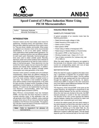
  • 10. AN843 System Overview time between the respective higher and lower PWMs. This driver needs an enable signal, which is controlled Figure 8 shows an overall block diagram of the power by the microcontroller. The IGBT driver has two FAULT and control circuit. A potentiometer is connected to AD monitoring circuits, one for over current and the second Channel 0. The PICmicro microcontroller reads this for under voltage. Upon any of these FAULTS, the out- input periodically to get the new speed or frequency ref- puts are driven low and the FAULT pin shows that a erence. Based on this AD result, the firmware deter- FAULT has occurred. If the FAULT is due to the over mines the scaling factor for the PWM duty cycle. The current, it can be automatically reset after a fixed time Timer0 reload value is calculated based on this input to delay, based on the resistor and capacitor time determine the motor frequency. PWM1 and PWM2 are constant connected to the RCIN pin of the driver. the hardware PWMs (CCP1 and CCP2). PWM3 is the PWM generated by software. The output of these three The main 3-phase supply is rectified by using the PWMs are given to the higher and lower input pins of 3-phase diode bridge rectifier. The DC ripple is filtered the IGBT driver as shown in Figure 8. The IGBT driver by using an electrolytic capacitor. This DC bus is has inverters on the lower input pins and adds dead- connected to the IGBTs for inverting it to a V/f supply. FIGURE 8: BLOCK DIAGRAM OF 3-PHASE INDUCTION MOTOR CONTROL 3-Phase AC Input 3-Phase Diode Bridge Rectifier Capacitor PWM1 HIN1 HOut1 IGBTH1 Potentiometer ADC PWM2 HIN2 PWM3 HIN3 HOut2 IGBTH2 LIN1 HOut3 IGBTH3 3-Phase Induction Fwd/Rev LIN2 PIC18XXX Motor LIN3 LOut1 IGBTL1 IGBT Run/Stop En En Driver LOut2 IGBTL2 3-Phase Inverter FAULT FAULT LOut3 IGBTL3 CONCLUSION TABLE 1: MEMORY REQUIREMENTS To control the speed of a 3-phase induction motor in Memory Bytes open loop, supply voltage and frequency need to be Program 0.9 Kbytes varied with constant ratio to each other. A low cost solu- Data 36 bytes tion of this control can be implemented in a PICmicro microcontroller. This requires three PWMs to control a 3-phase inverter bridge. Many PICmicro micro- controllers have two hardware PWMs. The third PWM is generated in software and output to a port pin. DS00843A-page 10  2002 Microchip Technology Inc.
  • 11. AN843 APPENDIX A: TEST RESULTS TABLE A-1: TEST RESULTS Test # Set Frequency (Hz) Set Speed (RPM) Actual Speed (RPM) Speed Regulation (%) 1 7.75 223 208 -1.875 2 10.5 302 286 -0.89 3 13.25 381 375 -0.33 4 16.75 482 490 +0.44 5 19.0 546 548 +0.11 6 20.75 597 590 +0.39 7 24.0 690 668 -1.22 8 27.0 776 743 -1.83 9 29.0 834 834 0.0 10 33.0 949 922 -1.5 11 38.0 1092 1078 0.78 12 45.75 1315 1307 -0.44 13 55.5 1596 1579 -0.94 14 58.25 1675 1644 -1.72 15 60 1725 1712 -0.72 Above tests are conducted on the motor with the following specifications: • Terminal voltage: 208-220 Volts • Frequency: 60 Hz • Horsepower: ½ HP • Speed: 1725 RPM • Current: 2.0 Amps • Frame: 56 NEMA  2002 Microchip Technology Inc. DS00843A-page 11
  • 12. U1 U2 FIGURE B-1: 11 10 VDD 20 +5V VDD RE2 VDD AN843 DS00843A-page 12 VDD 32 9 21 VDD RE1 RB0 APPENDIX B: 8 1 22 RE0 MCLR MCLR RB1 1 30 23 MCLR MCLR RD7 RB2 R3 29 2 24 RD6 AN0 RA0 RB3 EN 4.7K 2 28 3 25 S1 AN0 RA0 RD5 RA1 RB4 FAULT D5 3 27 4 26 1 4 RA1 RD4 LED1 RA2 RB5 RB5 MCLR 4 22 5 2 3 LED1 RA2 RD3 LED2 RA3 RB6 27 RB6 1N914 5 6 LED2 RA3 RD2 S2 RA4 RB7 28 RB7 C14 6 20 7 RA5 S2 RA4 RD1 S1 0.1 µF 7 19 11 S1 RA5 RD0 RC0 33 RB0 26 RXD RC1 12 RC1 RC7 34 RB1 25 RC2 13 RC6 TXD RC2 35 24 OSC1 9 OSC1 RC3 14 RB2 RC5 RC3 CONTROL AND DISPLAY EN 36 23 RC4 15 RB3 RC4 37 RB4 RC3 18 RC3 16 FAULT RC5 VDD VDD FAULT 38 17 17 RB5 RB5 RC2 RC2 OSC2 10 OSC2 RC6 TXD 39 16 18 C10 C11 C22 RB6 RB6 RC1 RC1 RC7 RXD 40 15 8 RB7 RB7 RC0 VSS 0.1 µF 0.1 µF 0.1 µF 19 VSS VSS OSC2 14 OSC2 PIC16C73 U1-12,12 U1-32,31 U2-7 13 VSS OSC1 OSC1 MOTOR CONTROL SCHEMATICS VSS VSS PIC18F452 +5V R5 D1 LED1 470 R8 4.7K R9 4.7K R6 D2 LED2 OSC2 470 S1 S2 Y1 OSC1 CW S2 S3 20 MHz R2 AN0 C12 C13 5K R1 4.7K R10 10K CCW 15 pF 15 pF  2002 Microchip Technology Inc.
  • 13. FIGURE B-2:  2002 Microchip Technology Inc. +20V POWER SUPPLY R7 10K Optional VR2 CN5 LM340T-5.0 +5V 1 1 Jumper IN OUT 3 VDD 2 R22 6.8K COM 2 D6 C24 C23 C25 100 µF 0.1 µF 0.1 µF R40 470 VSS AN843 DS00843A-page 13
  • 14. FIGURE B-3: +20V AN843 DS00843A-page 14 U3 1 C20 C19 VCC J1 U6 RC2 1 2 2 1 HIN1 K A R23 R24 R25 RC1 3 4 3 HIN2 2 5 6 4 D12 R11 3 RC3 HIN3 HO1 27 7 8 5 4 LIN1 LO1 16 K A 9 10 6 5 LIN2 D11 R12 +20V 11 12 7 HO2 23 6 LIN3 C27 C28 C29 7 POWER SECTION CN1 LO2 15 K A 8 1 19 D10 R13 9 R20 HO3 2 10 3 LO3 14 K A 11 11 D9 R14 IR21362_DIP28 RCIN 12 8 FAULT COM 13 13 CPV364M4U 10 M1 C21 EN K A 14 9 VSS 12 R27 R28 R29 M2 ITRIP D8 R15 15 M3 28 VB1 16 K A CN2 17 1 D4 R16 18 DC+ 2 VB3 VS3 VS1 VB2 VS2 19 C30 C31 C32 3 DC- 20 18 26 24 22 U5 C15 +5V P1 P2 R17 CN3 C18 P5 CN4 AC1 1 470 R41 1 1Ω, 2W R21 AC2 2 2 R18 R19 3 C8 C9 C16 C17 M3 AC3 3 P4 M2 D7 FAULT P6 P3 M1 EN K K +20V K D13 D14 D15 A A A CN6 1 C26 2 C7 C1 +20V AGND  2002 Microchip Technology Inc.
  • 15. AN843 APPENDIX C: GLOSSARY Locked Rotor Torque Starting torque of the motor. Air Gap Uniform gap between the stator and rotor. Pull-up Torque Torque available on the rotor at around 20% of base Angular Velocity speed. Velocity in radians (2π x frequency). Rotor Asynchronous Motor Rotating part of the motor. Type of motor in which the flux generated by the stator and rotor have different frequencies. Slip Speed Synchronous speed minus base speed. Base Speed Speed specified on the nameplate of an induction Stator motor. Stationary part of the motor. Break Down Torque Synchronous Motor Maximum torque on the speed-torque characteristics Type of motor in which the flux generated by the stator at approximately 80% of base speed. and rotor have the same frequencies. The phase may be shifted. EMF Electromotive Force. The potential generated by a cur- Synchronous Speed rent carrying conductor when it is exposed to magnetic Speed of the motor corresponding to the rated field. EMF is measured in volts. frequency. Full Load Torque Torque Rated torque of the motor as specified on the Rotating force in Newton-Meters or Pound-Inches. nameplate. IGBT Insulated Gate Bipolar Transistor. Lenz’s Law The Electromotive force (EMF) induced in a conductor moving perpendicular to a magnetic field tends to oppose that motion.  2002 Microchip Technology Inc. DS00843A-page 15
  • 16. AN843 APPENDIX D: SOFTWARE DISCUSSED IN THIS TECHNICAL BRIEF Because of its overall length, a complete source file list- ing is not provided. The complete source code is avail- able as a single WinZip archive file, which may be downloaded from the Microchip corporate web site at: www.microchip.com DS00843A-page 16  2002 Microchip Technology Inc.
  • 17. Note the following details of the code protection feature on PICmicro® MCUs. • The PICmicro family meets the specifications contained in the Microchip Data Sheet. • Microchip believes that its family of PICmicro microcontrollers is one of the most secure products of its kind on the market today, when used in the intended manner and under normal conditions. • There are dishonest and possibly illegal methods used to breach the code protection feature. All of these methods, to our knowl- edge, require using the PICmicro microcontroller in a manner outside the operating specifications contained in the data sheet. The person doing so may be engaged in theft of intellectual property. • Microchip is willing to work with the customer who is concerned about the integrity of their code. • Neither Microchip nor any other semiconductor manufacturer can guarantee the security of their code. Code protection does not mean that we are guaranteeing the product as “unbreakable”. • Code protection is constantly evolving. We at Microchip are committed to continuously improving the code protection features of our product. If you have any further questions about this matter, please contact the local sales office nearest to you. Information contained in this publication regarding device Trademarks applications and the like is intended through suggestion only and may be superseded by updates. It is your responsibility to The Microchip name and logo, the Microchip logo, FilterLab, ensure that your application meets with your specifications. KEELOQ, microID, MPLAB, PIC, PICmicro, PICMASTER, No representation or warranty is given and no liability is PICSTART, PRO MATE, SEEVAL and The Embedded Control assumed by Microchip Technology Incorporated with respect Solutions Company are registered trademarks of Microchip Tech- to the accuracy or use of such information, or infringement of nology Incorporated in the U.S.A. and other countries. patents or other intellectual property rights arising from such dsPIC, ECONOMONITOR, FanSense, FlexROM, fuzzyLAB, use or otherwise. Use of Microchip’s products as critical com- In-Circuit Serial Programming, ICSP, ICEPIC, microPort, ponents in life support systems is not authorized except with Migratable Memory, MPASM, MPLIB, MPLINK, MPSIM, express written approval by Microchip. No licenses are con- MXDEV, MXLAB, PICC, PICDEM, PICDEM.net, rfPIC, Select veyed, implicitly or otherwise, under any intellectual property Mode and Total Endurance are trademarks of Microchip rights. Technology Incorporated in the U.S.A. Serialized Quick Turn Programming (SQTP) is a service mark of Microchip Technology Incorporated in the U.S.A. All other trademarks mentioned herein are property of their respective companies. © 2002, Microchip Technology Incorporated, Printed in the U.S.A., All Rights Reserved. Printed on recycled paper. Microchip received QS-9000 quality system certification for its worldwide headquarters, design and wafer fabrication facilities in Chandler and Tempe, Arizona in July 1999 and Mountain View, California in March 2002. The Company’s quality system processes and procedures are QS-9000 compliant for its PICmicro® 8-bit MCUs, KEELOQ® code hopping devices, Serial EEPROMs, microperipherals, non-volatile memory and analog products. In addition, Microchip’s quality system for the design and manufacture of development systems is ISO 9001 certified.  2002 Microchip Technology Inc. DS00843A - page 17
  • 18. M WORLDWIDE SALES AND SERVICE AMERICAS ASIA/PACIFIC Japan Microchip Technology Japan K.K. Corporate Office Australia Benex S-1 6F 2355 West Chandler Blvd. Microchip Technology Australia Pty Ltd 3-18-20, Shinyokohama Chandler, AZ 85224-6199 Suite 22, 41 Rawson Street Kohoku-Ku, Yokohama-shi Tel: 480-792-7200 Fax: 480-792-7277 Epping 2121, NSW Kanagawa, 222-0033, Japan Technical Support: 480-792-7627 Australia Tel: 81-45-471- 6166 Fax: 81-45-471-6122 Web Address: http://www.microchip.com Tel: 61-2-9868-6733 Fax: 61-2-9868-6755 Korea Rocky Mountain China - Beijing Microchip Technology Korea 2355 West Chandler Blvd. Microchip Technology Consulting (Shanghai) 168-1, Youngbo Bldg. 3 Floor Chandler, AZ 85224-6199 Co., Ltd., Beijing Liaison Office Samsung-Dong, Kangnam-Ku Tel: 480-792-7966 Fax: 480-792-4338 Unit 915 Seoul, Korea 135-882 Bei Hai Wan Tai Bldg. Atlanta No. 6 Chaoyangmen Beidajie Tel: 82-2-554-7200 Fax: 82-2-558-5934 500 Sugar Mill Road, Suite 200B Beijing, 100027, No. China Singapore Atlanta, GA 30350 Tel: 86-10-85282100 Fax: 86-10-85282104 Microchip Technology Singapore Pte Ltd. Tel: 770-640-0034 Fax: 770-640-0307 200 Middle Road China - Chengdu Boston #07-02 Prime Centre Microchip Technology Consulting (Shanghai) Singapore, 188980 2 Lan Drive, Suite 120 Co., Ltd., Chengdu Liaison Office Tel: 65-6334-8870 Fax: 65-6334-8850 Westford, MA 01886 Rm. 2401, 24th Floor, Tel: 978-692-3848 Fax: 978-692-3821 Ming Xing Financial Tower Taiwan Chicago No. 88 TIDU Street Microchip Technology (Barbados) Inc., 333 Pierce Road, Suite 180 Chengdu 610016, China Taiwan Branch Itasca, IL 60143 Tel: 86-28-86766200 Fax: 86-28-86766599 11F-3, No. 207 Tel: 630-285-0071 Fax: 630-285-0075 Tung Hua North Road China - Fuzhou Taipei, 105, Taiwan Dallas Microchip Technology Consulting (Shanghai) 4570 Westgrove Drive, Suite 160 Tel: 886-2-2717-7175 Fax: 886-2-2545-0139 Co., Ltd., Fuzhou Liaison Office Addison, TX 75001 Unit 28F, World Trade Plaza Tel: 972-818-7423 Fax: 972-818-2924 No. 71 Wusi Road Detroit EUROPE Fuzhou 350001, China Tri-Atria Office Building Tel: 86-591-7503506 Fax: 86-591-7503521 Austria 32255 Northwestern Highway, Suite 190 Microchip Technology Austria GmbH China - Shanghai Farmington Hills, MI 48334 Durisolstrasse 2 Microchip Technology Consulting (Shanghai) Tel: 248-538-2250 Fax: 248-538-2260 A-4600 Wels Co., Ltd. Kokomo Austria Room 701, Bldg. B 2767 S. Albright Road Tel: 43-7242-2244-399 Far East International Plaza Kokomo, Indiana 46902 Fax: 43-7242-2244-393 No. 317 Xian Xia Road Tel: 765-864-8360 Fax: 765-864-8387 Shanghai, 200051 Denmark Los Angeles Tel: 86-21-6275-5700 Fax: 86-21-6275-5060 Microchip Technology Nordic ApS Regus Business Centre 18201 Von Karman, Suite 1090 China - Shenzhen Irvine, CA 92612 Lautrup hoj 1-3 Microchip Technology Consulting (Shanghai) Ballerup DK-2750 Denmark Tel: 949-263-1888 Fax: 949-263-1338 Co., Ltd., Shenzhen Liaison Office Tel: 45 4420 9895 Fax: 45 4420 9910 New York Rm. 1315, 13/F, Shenzhen Kerry Centre, 150 Motor Parkway, Suite 202 Renminnan Lu France Hauppauge, NY 11788 Shenzhen 518001, China Microchip Technology SARL Tel: 631-273-5305 Fax: 631-273-5335 Tel: 86-755-2350361 Fax: 86-755-2366086 Parc d’Activite du Moulin de Massy 43 Rue du Saule Trapu San Jose China - Hong Kong SAR Batiment A - ler Etage Microchip Technology Inc. Microchip Technology Hongkong Ltd. 91300 Massy, France 2107 North First Street, Suite 590 Unit 901-6, Tower 2, Metroplaza Tel: 33-1-69-53-63-20 Fax: 33-1-69-30-90-79 San Jose, CA 95131 223 Hing Fong Road Tel: 408-436-7950 Fax: 408-436-7955 Germany Kwai Fong, N.T., Hong Kong Microchip Technology GmbH Toronto Tel: 852-2401-1200 Fax: 852-2401-3431 Gustav-Heinemann Ring 125 6285 Northam Drive, Suite 108 India D-81739 Munich, Germany Mississauga, Ontario L4V 1X5, Canada Microchip Technology Inc. Tel: 49-89-627-144 0 Fax: 49-89-627-144-44 Tel: 905-673-0699 Fax: 905-673-6509 India Liaison Office Italy Divyasree Chambers Microchip Technology SRL 1 Floor, Wing A (A3/A4) Centro Direzionale Colleoni No. 11, O’Shaugnessey Road Palazzo Taurus 1 V. Le Colleoni 1 Bangalore, 560 025, India 20041 Agrate Brianza Tel: 91-80-2290061 Fax: 91-80-2290062 Milan, Italy Tel: 39-039-65791-1 Fax: 39-039-6899883 United Kingdom Microchip Ltd. 505 Eskdale Road Winnersh Triangle Wokingham Berkshire, England RG41 5TU Tel: 44 118 921 5869 Fax: 44-118 921-5820 05/16/02 DS00843A-page 18  2002 Microchip Technology Inc.