Measures of Dispersion and Variability: Range, QD, AD and SD
AT89 S52
1. 2.1 AT89S52
2.2.1 A BRIEF HISTORY OF 8051
In 1981, Intel Corporation introduced an 8 bit microcontroller called 8051. This
microcontroller had 128 bytes of RAM, 4K bytes of chip ROM, two timers, one serial port, and
four ports all on a single chip. At the time it was also referred as “A SYSTEM ON A CHIP”
AT89S52:
The AT89S52 is a low-power, high-performance CMOS 8-bit microcontroller with 8K bytes of
in-system programmable Flash memory. The device is manufactured using Atmel’s high-density
nonvolatile memory technology and is compatible with the industry-standard 80C51 instruction
set and pinout. The on-chip Flash allows the program memory to be reprogrammed in-system or
by a conventional nonvolatile memory pro-grammer. By combining a versatile 8-bit CPU with
in-system programmable Flash on a monolithic chip, the Atmel AT89S52 is a powerful
microcontroller, which provides a highly flexible and cost-effective solution to many, embedded
control applications. The AT89S52 provides the following standard features: 8K bytes of Flash,
256 bytes of RAM, 32 I/O lines, Watchdog timer, two data pointers, three 16-bit timer/counters,
a six-vector two-level interrupt architecture, a full duplex serial port, on-chip oscillator, and
clock circuitry. In addition, the AT89S52 is designed with static logic for operation down to zero
frequency and supports two software selectable power saving modes. The Idle Mode stops the
CPU while allowing the RAM, timer/counters, serial port, and interrupt system to continue
functioning. The Power-down mode saves the RAM con-tents but freezes the oscillator,
disabling all other chip functions until the next interrupt
2. • 8031 has 128 bytes of RAM, two timers and 6 interrupts.
• 8051 has 4K ROM, 128 bytes of RAM, two timers and 6 interrupts.
• 8052 has 8K ROM, 256 bytes of RAM, three timers and 8 interrupts.
Of the three microcontrollers, 8051 is the most preferable. Microcontroller supports both
serial and parallel communication.
In the concerned project 8052 microcontroller is used. Here microcontroller used is
AT89S52, which is manufactured by ATMEL laboratories.
The 8051 is the name of a big family of microcontrollers. The device which we are going
to use along this tutorial is the 'AT89S52' which is a typical 8051 microcontroller manufactured
by Atmel™. Note that this part doesn't aim to explain the functioning of the different
components of a 89S52 microcontroller, but rather to give you a general idea of the organization
of the chip and the available features, which shall be explained in detail along this tutorial.
The block diagram provided by Atmel™ in their datasheet showing the architecture the 89S52
device can seem very complicated, and since we are going to use the C high level language to
3. program it, a simpler architecture can be represented as the figure 1.2.A.
This figures shows the main features and components that the designer can interact with. You
can notice that the 89S52 has 4 different ports, each one having 8 Input/output lines providing a
total of 32 I/O lines. Those ports can be used to output DATA and orders do other devices, or to
read the state of a sensor, or a switch. Most of the ports of the 89S52 have 'dual function'
meaning that they can be used for two different functions: the fist one is to perform input/output
operations and the second one is used to implement special features of the microcontroller like
counting external pulses, interrupting the execution of the program according to external events,
performing serial data transfer or connecting the chip to a computer to update the software.
NECESSITY OF MICROCONTROLLERS:
Microprocessors brought the concept of programmable devices and made many
applications of intelligent equipment. Most applications, which do not need large amount of data
and program memory, tended to be costly.
The microprocessor system had to satisfy the data and program requirements so,
sufficient RAM and ROM are used to satisfy most applications .The peripheral control
equipment also had to be satisfied. Therefore, almost all-peripheral chips were used in the
design. Because of these additional peripherals cost will be comparatively high.
An example:
8085 chip needs:
An Address latch for separating address from multiplex address and data.32-KB RAM and
32-KB ROM to be able to satisfy most applications. As also Timer / Counter, Parallel
programmable port, Serial port, and Interrupt controller are needed for its efficient applications.
In comparison a typical Micro controller 8051 chip has all that the 8051 board has except
a reduced memory as follows.
4K bytes of ROM as compared to 32-KB, 128 Bytes of RAM as compared to 32-KB.
Bulky:
4. On comparing a board full of chips (Microprocessors) with one chip with all components
in it (Microcontroller).
Debugging:
Lots of Microprocessor circuitry and program to debug. In Micro controller there is no
Microprocessor circuitry to debug.
Slower Development time: As we have observed Microprocessors need a lot of debugging at
board level and at program level, where as, Micro controller do not have the excessive circuitry
and the built-in peripheral chips are easier to program for operation.
So peripheral devices like Timer/Counter, Parallel programmable port, Serial
Communication Port, Interrupt controller and so on, which were most often used were integrated
with the Microprocessor to present the Micro controller .RAM and ROM also were integrated in
the same chip. The ROM size was anything from 256 bytes to 32Kb or more. RAM was
optimized to minimum of 64 bytes to 256 bytes or more.
Microprocessor has following instructions to perform:
1. Reading instructions or data from program memory ROM.
2. Interpreting the instruction and executing it.
3. Microprocessor Program is a collection of instructions stored in a Nonvolatile memory.
4. Read Data from I/O device
5. Process the input read, as per the instructions read in program memory.
6. Read or write data to Data memory.
7. Write data to I/O device and output the result of processing to O/P device.
2.1.2 Introduction to AT89S52
The system requirements and control specifications clearly rule out the use of 16, 32 or 64
bit micro controllers or microprocessors. Systems using these may be earlier to implement due to
large number of internal features. They are also faster and more reliable but, the above
application is satisfactorily served by 8-bit micro controller. Using an inexpensive 8-bit
Microcontroller will doom the 32-bit product failure in any competitive market place. Coming to
the question of why to use 89S52 of all the 8-bit Microcontroller available in the market the main
5. answer would be because it has 8kB Flash and 256 bytes of data RAM32 I/O lines, three 16-bit
timer/counters, a Eight-vector two-level interrupt architecture, a full duplex serial port, on-chip
oscillator, and clock circuitry.
In addition, the AT89S52 is designed with static logic for operation down to zero
frequency and supports two software selectable power saving modes. The Idle Mode stops the
CPU while allowing the RAM, timer/counters, serial port, and interrupt system to continue
functioning. The Power Down Mode saves the RAM contents but freezes the oscillator, disabling
all other chip functions until the next hardware reset. The Flash program memory supports both
parallel programming and in Serial In-System Programming (ISP). The 89S52 is also In-
Application Programmable (IAP), allowing the Flash program memory to be reconfigured even
while the application is running.
By combining a versatile 8-bit CPU with Flash on a monolithic chip, the Atmel AT89S52 is
a powerful microcomputer which provides a highly flexible and cost effective solution to many
embedded control applications.
2.1.3 FEATURES
Compatible with MCS-51 Products
8K Bytes of In-System Reprogrammable Flash Memory
Fully Static Operation: 0 Hz to 33 MHz
Three-level Program Memory Lock
256 x 8-bit Internal RAM
32 Programmable I/O Lines
Three 16-bit Timer/Counters
Eight Interrupt Sources
Programmable Serial Channel
Low-power Idle and Power-down Modes
4.0V to 5.5V Operating Range
Full Duplex UART Serial Channel
Interrupt Recovery from Power-down Mode
Watchdog Timer
6. Dual Data Pointer
Power-off Flag
Fast Programming Time
Flexible ISP Programming (Byte and Page Mode)
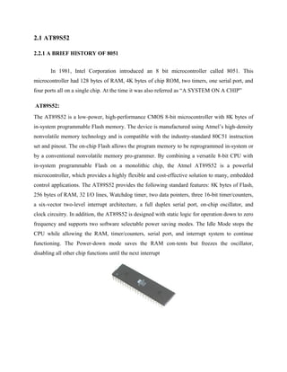
2.1.4 PIN DIAGRAM
FIG-2 PIN DIAGRAM OF 89S52 IC
2.1.5 PIN DESCRIPTION
Pin Description
VCC
7. Supply voltage.
GND
Ground.
Port 0
Port 0 is an 8-bit open drain bidirectional I/O port. As an output port, each pin can sink eight
TTL inputs. When 1s are written to port 0 pins, the pins can be used as highimpedance
inputs.Port 0 can also be configured to be the multiplexed loworder address/data bus during
accesses to external program and data memory. In this mode, P0 has internal pullups. Port 0 also
receives the code bytes during Flash programming and outputs the code bytes during program
verification.
External pullups are required during program verification.
Port 1
Port 1 is an 8-bit bidirectional I/O port with internal pullups. The Port 1 output buffers can
sink/source four TTL inputs. When 1s are written to Port 1 pins, they are pulled high by the
internal pullups and can be used as inputs. As inputs,Port 1 pins that are externally being pulled
low will source current (IIL) because of the internal pullups. In addition, P1.0 and P1.1 can be
configured to be the timer/counter 2 external count input (P1.0/T2) and the timer/counter 2
trigger input (P1.1/T2EX), respectively, as shown in the following table. Port 1 also receives the
low-order address bytes during Flash programming and verification.
Port 2
Port 2 is an 8-bit bidirectional I/O port with internal pullups.The Port 2 output buffers can
sink/source four TTL inputs.When 1s are written to Port 2 pins, they are pulled high by
the internal pullups and can be used as inputs. As inputs, Port 2 pins that are externally being
pulled low will source current (IIL) because of the internal pullups. Port 2 emits the high-order
address byte during fetches from external program memory and during accesses to external data
8. memory that use 16-bit addresses (MOVX @ DPTR). In this application, Port 2 uses strong
internal pull-ups when emitting 1s. During accesses to external data memory that use 8-bit
addresses (MOVX @ RI), Port 2 emits the contents of the P2 Special Function Register. Port 2
also receives the high-order address bits and some control signals during Flash programming and
verification.
Port 3
Port 3 is an 8-bit bidirectional I/O port with internal pullups.The Port 3 output buffers can
sink/source four TTL inputs. When 1s are written to Port 3 pins, they are pulled high by the
internal pullups and can be used as inputs. As inputs, Port 3 pins that are externally being pulled
low will source current (IIL) because of the pullups. Port 3 also serves the functions of various
special features of the AT89S52, as shown in the following table. Port 3 also receives some
control signals for Flash programming and verification.
RST
Reset input. A high on this pin for two machine cycles while the oscillator is running resets the
device. This pin drives High for 96 oscillator periods after the Watchdog times out. The DISRTO
bit in SFR AUXR (address 8EH) can be used to disable this feature. In the default state of bit
DISRTO, the RESET HIGH out feature is enabled. ALE/PROG Address Latch Enable (ALE) is
an output pulse for latching the low byte of the address during accesses to external memory. This
pin is also the program pulse input (PROG) during Flash programming. In normal operation,
ALE is emitted at a constant rate of 1/6 the oscillator frequency and may be used for external
timing or clocking purposes. Note, however, that one ALE pulse is skipped during each access to
external data memory. If desired, ALE operation can be disabled by setting bit 0 of SFR location
8EH. With the bit set, ALE is active only during a MOVX or MOVC instruction. Otherwise, the
9. pin is weakly pulled high. Setting the ALE-disable bit has no effect if the microcontroller is in
external execution mode.
PSEN
Program Store Enable (PSEN) is the read strobe to external program memory. When the
AT89S52 is executing code from external program memory, PSEN is activated twice each
machine cycle, except that two PSEN activations are skipped during each access to external data
memory.
EA/VPP
External Access Enable. EA must be strapped to GND in order to enable the device to fetch code
from external program memory locations starting at 0000H up to FFFFH. Note, however, that if
lock bit 1 is programmed, EA will be internally latched on reset. EA should be strapped to VCC
for internal program executions. This pin also receives the 12-volt programming enable voltage
(VPP) during Flash programming.
XTAL1
Input to the inverting oscillator amplifier and input to the
internal clock operating circuit.
XTAL2
Output from the inverting oscillator amplifier.
10. FIG-3 Functional block diagram of micro controller
The 8052 Oscillator and Clock:
The heart of the 8051 circuitry that generates the clock pulses by which all the
internal all internal operations are synchronized. Pins XTAL1 And XTAL2 is provided for
connecting a resonant network to form an oscillator. Typically a quartz crystal and capacitors are
employed. The crystal frequency is the basic internal clock frequency of the microcontroller. The
manufacturers make 8051 designs that run at specific minimum and maximum frequencies
typically 1 to 16 MHz.
11. Fig-4 Oscillator and timing circuit
MEMORIES
Types of memory:
The 8052 have three general types of memory. They are on-chip memory, external Code
memory and external Ram. On-Chip memory refers to physically existing memory on the micro
controller itself. External code memory is the code memory that resides off chip. This is often in
the form of an external EPROM. External RAM is the Ram that resides off chip. This often is in
the form of standard static RAM or flash RAM.
12. a) Code memory
Code memory is the memory that holds the actual 8052 programs that is to be run. This
memory is limited to 64K. Code memory may be found on-chip or off-chip. It is possible to have
8K of code memory on-chip and 60K off chip memory simultaneously. If only off-chip memory
is available then there can be 64K of off chip ROM. This is controlled by pin provided as EA
b) Internal RAM
The 8052 have a bank of 256 bytes of internal RAM. The internal RAM is found on-chip.
So it is the fastest Ram available. And also it is most flexible in terms of reading and writing.
Internal Ram is volatile, so when 8051 is reset, this memory is cleared. 256 bytes of internal
memory are subdivided. The first 32 bytes are divided into 4 register banks. Each bank contains
8 registers. Internal RAM also contains 256 bits, which are addressed from 20h to 2Fh. These
bits are bit addressed i.e. each individual bit of a byte can be addressed by the user. They are
numbered 00h to FFh. The user may make use of these variables with commands such as SETB
and CLR.
Special Function registered memory:
Special function registers are the areas of memory that control specific functionality of
the 8052 micro controller.
a) Accumulator (0E0h)
As its name suggests, it is used to accumulate the results of large no of instructions. It can
hold 8 bit values.
b) B registers (0F0h)
The B register is very similar to accumulator. It may hold 8-bit value. The b register is
only used by MUL AB and DIV AB instructions. In MUL AB the higher byte of the product gets
stored in B register. In div AB the quotient gets stored in B with the remainder in A.
13. c) Stack pointer (81h)
The stack pointer holds 8-bit value. This is used to indicate where the
next value to be removed from the stack should be taken from. When a value is to be pushed
onto the stack, the 8052 first store the value of SP and then store the value at the resulting
memory location. When a value is to be popped from the stack, the 8052 returns the value from
the memory location indicated by SP and then decrements the value of SP.
d) Data pointer
The SFRs DPL and DPH work together work together to represent a 16-bit value called
the data pointer. The data pointer is used in operations regarding external RAM and some
instructions code memory. It is a 16-bit SFR and also an addressable SFR.
e) Program counter
The program counter is a 16 bit register, which contains the 2 byte address, which tells
the 8052 where the next instruction to execute to be found in memory. When the 8052 is
initialized PC starts at 0000h. And is incremented each time an instruction is executes. It is not
addressable SFR.
f) PCON (power control, 87h)
The power control SFR is used to control the 8051’s power control modes. Certain
operation modes of the 8051 allow the 8051 to go into a type of “sleep mode” which consumes
much lee power.
g) TCON (timer control, 88h)
14. The timer control SFR is used to configure and modify the way in which the 8051’s two
timers operate. This SFR controls whether each of the two timers is running or stopped and
contains a flag to indicate that each timer has overflowed. Additionally, some non-timer related
bits are located in TCON SFR. These bits are used to configure the way in which the external
interrupt flags are activated, which are set when an external interrupt occurs.
h) TMOD (Timer Mode, 89h)
The timer mode SFR is used to configure the mode of operation of each of the two
timers. Using this SFR your program may configure each timer to be a 16-bit timer, or 13 bit
timer, 8-bit auto reload timer, or two separate timers. Additionally you may configure the timers
to only count when an external pin is activated or to count “events” that are indicated on an
external pin.
i) TO (Timer 0 low/high, address 8A/8C h)
These two SFRs taken together represent timer 0. Their exact behavior depends on how
the timer is configured in the TMOD SFR; however, these timers always count up. What is
configurable is how and when they increment in value.
j) T1 (Timer 1 Low/High, address 8B/ 8D h)
15. These two SFRs, taken together, represent timer 1. Their exact behavior depends on how
the timer is configured in the TMOD SFR; however, these timers always count up..
k) P0 (Port 0, address 90h, bit addressable)
This is port 0 latch. Each bit of this SFR corresponds to one of the pins on a micro
controller. Any data to be outputted to port 0 is first written on P0 register. For e.g., bit 0 of port
0 is pin P0.0, bit 7 is pin p0.7. Writing a value of 1 to a bit of this SFR will send a high level on
the corresponding I/O pin whereas a value of 0 will bring it to low level.
l) P1 (port 1, address 90h, bit addressable)
This is port latch1. Each bit of this SFR corresponds to one of the pins on a micro
controller. Any data to be outputted to port 0 is first written on P0 register. For e.g., bit 0 of port
0 is pin P1.0, bit 7 is pin P1.7. Writing a value of 1 to a bit of this SFR will send a high level on
the corresponding I/O pin whereas a value of 0 will bring it to low level
m) P2 (port 2, address 0A0h, bit addressable):
This is a port latch2. Each bit of this SFR corresponds to one of the pins on a micro
controller. Any data to be outputted to port 0 is first written on P0 register. For e.g., bit 0 of port
0 is pin P2.0, bit 7 is pin P2.7. Writing a value of 1 to a bit of this SFR will send a high level on
the corresponding I/O pin whereas a value of 0 will bring it to low level.
n) P3 (port 3, address B0h, bit addressable) :
This is a port latch3. Each bit of this SFR corresponds to one of the pins on a micro
controller. Any data to be outputted to port 0 is first written on P0 register. For e.g., bit 0 of port
0 is pin P3.0, bit 7 is pin P3.7. Writing a value of 1 to a bit of this SFR will send a high level on
the corresponding I/O pin whereas a value of 0 will bring it to low level.
o) IE (interrupt enable, 0A8h):
16. The Interrupt Enable SFR is used to enable and disable specific interrupts. The low 7 bits
of the SFR are used to enable/disable the specific interrupts, where the MSB bit is used to enable
or disable all the interrupts. Thus, if the high bit of IE is 0 all interrupts are disabled regardless of
whether an individual interrupt is enabled by setting a lower bit.
p) IP (Interrupt Priority, 0B8h)
The interrupt priority SFR is used to specify the relative priority of each interrupt. On
8051, an interrupt maybe either low or high priority. An interrupt may interrupt interrupts. For
e.g., if we configure all interrupts as low priority other than serial interrupt. The serial interrupt
always interrupts the system, even if another interrupt is currently executing. However, if a serial
interrupt is executing no other interrupt will be able to interrupt the serial interrupt routine since
the serial interrupt routine has the highest priority.
q) PSW (Program Status Word, 0D0h)
The program Status Word is used to store a number of important bits that are set and
cleared by 8052 instructions. The PSW SFR contains the carry flag, the auxiliary carry flag, the
parity flag and the overflow flag. Additionally, it also contains the register bank select flags,
which are used to select, which of the “R” register banks currently in use.
r) SBUF (Serial Buffer, 99h)
SBUF is used to hold data in serial communication. It is physically two registers. One is
writing only and is used to hold data to be transmitted out of 8052 via TXD. The other is read
only and holds received data from external sources via RXD. Both mutually exclusive registers
use address 99h.