SlideShare uma empresa Scribd logo
1 de 94
Baixar para ler offline
Supplement to InfiniBandTM
                         Architecture Specification
                            Volume 2 Release 1.2.1


            Annex A6:
   120 Gb/s 12x Small
Form-factor Pluggable
                (CXP)

Interface Specification for
    Cables, Active Cables,
           & Transceivers

                                                               September 2009


Copyright © 2009 by the InfiniBandSM Trade Association
All rights reserved.
All trademarks and brands are the property of their respective owners.
InfiniBandTM Architecture - Annex A6                                              September 2009
VOLUME 2 - PHYSICAL SPECIFICATIONS                                                 FINAL RELEASE


                                                                                                        1
                                           Table 0 Revision History
                                                                                                        2
 Revision        Date                                        Revisions
                                                                                                        3
    1.0        9/18/2009    Released Version
                                                                                                        4

                                                                                                        5

                                                                                                        6

                                                                                                        7
LEGAL DISCLAIMER                       This specification provided “AS IS” and without any
                                                                                                        8
                                       warranty of any kind, including, without limitation,
                                       any express or implied warranty of non-infringement,             9
                                       merchantability or fitness for a particular purpose.
                                                                                                        10

                                       In no event shall IBTA or any member of IBTA be liable           11
                                       for any direct, indirect, special, exemplary, punitive,
                                                                                                        12
                                       or consequential damages, including, without limita-
                                       tion, lost profits, even if advised of the possibility of        13
                                       such damages.
                                                                                                        14

                                                                                                        15

                                                                                                        16

                                                                                                        17

                                                                                                        18

                                                                                                        19

                                                                                                        20

                                                                                                        21

                                                                                                        22

                                                                                                        23

                                                                                                        24


InfiniBandSM Trade Association                     Page 2                           CXP Specification
InfiniBandTM Architecture - Annex A6                                                                                                     September 2009
VOLUME 2 - PHYSICAL SPECIFICATIONS                                                                                                        FINAL RELEASE

TABLE      OF     CONTENTS                                                                                                                                       1

                                                                                                                                                                 2

                                                                                                                                                                 3
Chapter 1:           Overview             ..........................................................................................8
1.1       Design Targets and Compatibility ...............................................................................8                                      4
1.2       Participants ...............................................................................................................11
                                                                                                                                                                 5
Chapter 2:           Electrical Specification                        ................................................................12
                                                                                                                                                                 6
2.1       Electrical Connector..................................................................................................12
2.2       Host board Schematic ..............................................................................................14                                  7
2.3       Low-Speed Electrical Contact/Signal Definitions ......................................................14
          2.3.1         SDA, SCL ............................................................................................................. 14                8
          2.3.2         Int_L/Reset_L ....................................................................................................... 14
                                                                                                                                                                 9
          2.3.3         PRSNT_L.............................................................................................................. 16
2.4       High-Speed Electrical Contact/Signal Definitions .....................................................16                                               10
          2.4.1         Receive Signals: Rx[0-11][p/n].............................................................................. 16
          2.4.2         Transmit Signals: Tx[0-11][p/n] ............................................................................. 17                         11
2.5       Power Requirements ................................................................................................17
          2.5.1         Host Power Supply Filtering.................................................................................. 17
                                                                                                                                                                 12
          2.5.2         Host Power Supply Specifications ........................................................................ 19
                                                                                                                                                                 13
          2.5.3         Power Budget Classes.......................................................................................... 19
2.6       ESD ..........................................................................................................................21                       14
2.7       Hot Insertion and Removal .......................................................................................21
                                                                                                                                                                 15
Chapter 3:           High-Speed Electrical Signaling                                  .................................................22
3.1       Introduction ...............................................................................................................22                         16
3.2       Compliance Points ....................................................................................................22                               17
3.3       Linear Passive / Linear Active Interface ...................................................................23
          3.3.1         Host Differential Driver Outputs ............................................................................ 23                         18
          3.3.2         Compliant Channel - Module Tx Inputs to Module Rx Outputs............................. 23
          3.3.3         Host Differential Receiver Inputs .......................................................................... 24                          19
3.4       Limiting Active Interface............................................................................................25
                                                                                                                                                                 20
          3.4.1         Host Differential Driver Outputs ............................................................................ 25
          3.4.2         CXP Module Tx Inputs .......................................................................................... 26                       21
          3.4.3         CXP Module Rx Outputs....................................................................................... 26
          3.4.4         Host Differential Receiver Inputs .......................................................................... 27                          22

                                                                                                                                                                 23

                                                                                                                                                                 24


InfiniBandSM Trade Association                                          Page 3                                                               CXP Specification
InfiniBandTM Architecture - Annex A6                                                                                                   September 2009
VOLUME 2 - PHYSICAL SPECIFICATIONS                                                                                                      FINAL RELEASE

Chapter 4:           Mechanical and Board Definition                                  ................................................28
                                                                                                                                                               1
4.1       Introduction ...............................................................................................................28
4.2       CXP Datums and Component Alignment .................................................................29                                               2
4.3       CXP Module Package Dimensions ...........................................................................31
                                                                                                                                                               3
4.4       Connector Orientation Key........................................................................................36
4.5       Host PCB Footprint ...................................................................................................36                             4
          4.5.1         Grounding Pad Structure ...................................................................................... 38
          4.5.2         Mating of CXP Module & Host PCBs to CXP Electrical Connectors.................... 38                                                   5
4.6       Bezel for Systems Using CXP Transceivers.............................................................40
                                                                                                                                                               6
Chapter 5:            Environmental and Thermal Specifications                                           ..............................41
                                                                                                                                                               7
5.1       Physical and Mechanical Performance Requirements .............................................41
5.2       Connector Electrical Performance Requirements.....................................................42                                                 8
5.3       Mechanical and Environmental Requirements .........................................................42
5.4       Thermal Performance Ranges..................................................................................43                                       9
5.5       CXP Housing Assembly Thermal Interfaces.............................................................44
                                                                                                                                                               10
5.6       EMI / Dust Cover for receptacle................................................................................49
                                                                                                                                                               11
Chapter 6:           Cable Design                 .................................................................................50
6.1       Device, Module, and Cable Options .........................................................................50                                        12
          6.1.1         Separable optical Transceiver .............................................................................. 50
          6.1.2         Active optical Cable .............................................................................................. 51                 13
          6.1.3         Copper Cable........................................................................................................ 51
                                                                                                                                                               14
6.2       Latch Release ...........................................................................................................52
6.3       Cable Connectivity ....................................................................................................53                            15
          6.3.1         Cable Connectivity Mapping ................................................................................. 53
          6.3.2         12x to 3-4x Cables ................................................................................................ 54                 16
6.4       Lane Usage for 10-lane Interface .............................................................................55
                                                                                                                                                               17
6.5       Media-Specific Requirements - Optical Transceivers and Optical Cables ................56
          6.5.1         Color Coding and Labeling of CXP Optical Transceivers ..................................... 56                                         18
          6.5.2         Optical Connector Interfaces for 24-fiber transceivers.......................................... 57
          6.5.3         Interface between 24-fiber connector and dual 12-fiber connectors..................... 58                                              19

Chapter 7:           Management Interface                         ..................................................................59                         20
7.1       Introduction ...............................................................................................................59
                                                                                                                                                               21
7.2       Voltage and Timing Specification ..............................................................................59
          7.2.1         Management interface Voltage Specification ........................................................ 59                                 22
          7.2.2         Management Interface Timing Specification ......................................................... 59
7.3       Memory Interaction Specifications ...........................................................................61                                      23
          7.3.1         Timing for Memory Transactions........................................................................... 61
          7.3.2         Timing for Control and Status Functions ............................................................... 62                             24


InfiniBandSM Trade Association                                         Page 4                                                              CXP Specification
InfiniBandTM Architecture - Annex A6                                                                                                 September 2009
VOLUME 2 - PHYSICAL SPECIFICATIONS                                                                                                    FINAL RELEASE

          7.3.3        Timing for Squelch and Disable Functions ........................................................... 63
                                                                                                                                                             1
7.4       Device Addressing and Operation ............................................................................64
7.5       Read/Write Functionality...........................................................................................65                              2
          7.5.1        CXP Memory Address Counter (Read AND Write Operations) ............................ 65
          7.5.2        Read Operations (Current Address Read)............................................................ 66                                 3
          7.5.3        Read Operations (Random Read) ........................................................................ 66
                                                                                                                                                             4
          7.5.4        Read Operations (Sequential Read)..................................................................... 67
          7.5.5        Write Operations (Byte Write) ............................................................................... 68                      5
          7.5.6        Write Operations (Sequential Write) ..................................................................... 69
          7.5.7        Write Operations (Acknowledge Polling) .............................................................. 70                              6
7.6       CXP Memory Map ....................................................................................................71
          7.6.1        Tx Lower Page...................................................................................................... 73                7
          7.6.2        Rx Lower Page ..................................................................................................... 79
                                                                                                                                                             8
          7.6.3        Tx & Rx Common Upper Page 00h ...................................................................... 85
          7.6.4        Tx Upper Page 01h............................................................................................... 91                   9
          7.6.5        Rx Upper Page 01h .............................................................................................. 92
                                                                                                                                                             10

                                                                                                                                                             11

                                                                                                                                                             12

                                                                                                                                                             13

                                                                                                                                                             14

                                                                                                                                                             15

                                                                                                                                                             16

                                                                                                                                                             17

                                                                                                                                                             18

                                                                                                                                                             19

                                                                                                                                                             20

                                                                                                                                                             21

                                                                                                                                                             22

                                                                                                                                                             23

                                                                                                                                                             24


InfiniBandSM Trade Association                                        Page 5                                                             CXP Specification
InfiniBandTM Architecture - Annex A6                                                                                      September 2009
VOLUME 2 - PHYSICAL SPECIFICATIONS                                                                                         FINAL RELEASE

LIST    OF   FIGURES                                                                                                                             1

                                                                                                                                                 2

                                                                                                                                                 3
Figure 1          CXP Conceptual Model ..................................................................................10
Figure 2          Example Host Board Schematic.....................................................................15                            4
Figure 3          Recommended Host Board Power Supply Filtering .......................................18
Figure 4          Application Reference Model and Compliance Points ...................................23                                        5
Figure 5          General view, CXP Cable Connector & Housing Assembly, w/o heat sink ....28
Figure 6          Cable Connector and Receptacle Housing Datums .......................................30                                        6
Figure 7          Shielded Free (Plug) Integrated Cable Connector .........................................31
Figure 8          Shielded Free (Plug) Integrated Cable Connector, cont’d..............................32                                        7
Figure 9          Paddle Card Dimensions and Definition of Datums .......................................33
Figure 10         Fixed (Receptacle) Connector........................................................................34                         8
Figure 11         Dimensions for Fixed (Receptacle) Connector in Figure 10...........................35
Figure 12         Connector Key................................................................................................36                9
Figure 13         Footprint - Shown in example application, Low Profile PCIe card..................37
Figure 14         Ground Pad - Shown in example application, Low Profile PCIe card ...........39                                                 10
Figure 15         Panel Cutout - Shown in example application, Low Profile PCIe card ..........40
Figure 16         Receptacle Housing with Integrated Riding Heat Sink ...................................44                                      11
Figure 17         Heat Sink Interface on Connector Plug ..........................................................45
Figure 18         Heat Sink Thermal Interface Profile ...............................................................46                          12
Figure 19         Heat Sink Clip Attach Points on Receptacle Housing ....................................47
Figure 20         Heat Sink Clip Structure .................................................................................48                   13
Figure 21         EMI cover / Dust Cover ..................................................................................49
Figure 22         Optical Transceiver with separable optical cable ...........................................50                                 14
Figure 23         Active Optical Cable .......................................................................................51
Figure 24         Passive or Active Copper Cable.....................................................................51                          15
Figure 25         Exemplary Latch Release Mechanism for a Cable Connector .......................52
Figure 26         12x to 3-4x cables ..........................................................................................54                16
Figure 27         Connector orientation for 24-fiber MPO/MTP connector ................................57
Figure 28         Connector interface between 24-fiber and Two 12-fiber connectors..............58                                               17
Figure 29         CXP 2-wire Serial Interface Timing Diagram..................................................60
Figure 30         CXP Device Addresses ..................................................................................65                      18
Figure 31         Read Operation on Current Address ..............................................................66
Figure 32         Random Read ................................................................................................67                 19
Figure 33         Sequential Address Read Starting at Current Address ..................................68
Figure 34         Sequential Address Read Starting with Random CXP Read .........................68                                              20
Figure 35         Write Byte Operation ......................................................................................69
Figure 36         Sequential Write Operation ............................................................................70                      21
Figure 37         Memory Map 2-Wire Serial Addresses 1010 000x (Tx) & 1010 100x (Rx) ...72
                                                                                                                                                 22

                                                                                                                                                 23

                                                                                                                                                 24


InfiniBandSM Trade Association                                  Page 6                                                       CXP Specification
InfiniBandTM Architecture - Annex A6                                                                                        September 2009
VOLUME 2 - PHYSICAL SPECIFICATIONS                                                                                           FINAL RELEASE

LIST    OF   TABLES                                                                                                                                1

                                                                                                                                                   2

                                                                                                                                                   3
Table 0          Revision History ................................................................................................2
Table 1          Representative Transmission Media and Link Lengths .....................................9                                         4
Table 2          Contact Assignments for 12x Pluggable-CXP Interface ..................................13
Table 3          Power Supply Specification .............................................................................19                        5
Table 4          Power Budget Classification............................................................................19
Table 5          Compliant Channel S Parameter Requirements for 10 Gb/s (QDR) ...............24                                                    6
Table 6          Driver Characteristics for 10 Gb/s, for Limiting Active interfaces ....................25
Table 7          CXP Limiting Active Module Tx Input Characteristics for 10 Gb/s ..................26                                              7
Table 8          CXP Limiting Active Module Rx Output Characteristics for 10 Gb/s ...............26
                                                                                                                                                   8
Table 9          Receiver Characteristics for 10 Gb/s...............................................................27
Table 10         Definition of Datums ........................................................................................29
                                                                                                                                                   9
Table 11         Module & Receptacle Connector Physical Requirements ...............................41
Table 12         Recommended Connector Physical Parameters ............................................41                                          10
Table 13         Module & Receptacle Connector Electrical Performance Requirements ........42
Table 14         Module and Receptacle Mechanical and Environmental Requirements .........43                                                       11
Table 15         Temperature Classification of Module Case....................................................44
Table 16         Cable Connector Signal Assignment...............................................................53                                12
Table 17         12x Board Connector Signal Assignment for 12x to 3-4x Cables ...................55
Table 18         Low Speed Control and Sense Signal Specifications......................................59                                         13
Table 19         CXP 2-Wire Serial Interface Timing Specifications..........................................60
Table 20         CXP Memory Transaction Timing Specification...............................................61                                      14
Table 21         I/O Timing for Control and Status Functions....................................................62
                                                                                                                                                   15
Table 22         I/O Timing for Squelch and Disable.................................................................63
Table 23         Tx Lower Page Memory Map ..........................................................................73
                                                                                                                                                   16
Table 24         Rx Lower Page Memory Map (Optional) .........................................................79
Table 25         Tx & Rx Upper Page 00h Memory Map ..........................................................85                                    17
Table 26         Tx Upper Page 01h Memory Map ...................................................................91
Table 27         Rx Upper Page 01h Memory Map ...................................................................92                                18

                                                                                                                                                   19

                                                                                                                                                   20

                                                                                                                                                   21

                                                                                                                                                   22

                                                                                                                                                   23

                                                                                                                                                   24


InfiniBandSM Trade Association                                   Page 7                                                        CXP Specification
InfiniBandTM Architecture - Annex A6                    Overview                                  September 2009
VOLUME 2 - PHYSICAL SPECIFICATIONS                                                                 FINAL RELEASE

CHAPTER 1:               OVERVIEW                                                                                       1

                                                                                                                        2

                                                                                                                      3
                                       This specification is a description of a 12x form-factor pluggable active de-
                                       vice interface, with 12 transmit and 12 receive lanes, capable of sup- 4
                                       porting bit-rates in excess of 10 Gb/s per lane on a variety of electrical and
                                       optical transmission technologies.                                             5

                                       This specification describes the form factor, electrical, mechanical, power,     6
                                       and thermal interfaces between the devices or cables and the systems.
                                       The transmission technology (e.g., optical or electronic), transmission          7
                                       medium (e.g., single-mode, multi-mode fiber, or copper), form factor (i.e.,
                                       with cable attached to the pluggable device, or detachable with a sepa-          8
                                       rable connector), and physical layer definition for the communication be-
                                       tween transceivers are not explicitly specified. However, the                    9
                                       specifications are intended to support several different technologies, in-
                                       cluding VCSEL/MMF parallel ribbon fiber links.                                   10

                                       The current primary target for this technology is the InfiniBand architec- 11
                                       ture, at the 12x-QDR (Quad Data Rate) rate, as well as DDR and SDR
                                       rates. Other standards, such as Ethernet at the 100 Gb/s data rate and 12
                                       Fibre Channel, may be supported as well.1
                                                                                                                  13
1.1 DESIGN TARGETS AND COMPATIBILITY
                                                                                                                14
                                       This paragraph describes the design targets of the device. These targets
                                       are used as foundation for making decisions regarding the design of the
                                                                                                                15
                                       interface and related devices.
                                                                                                               16
                                       •   Transmission Bandwidth: The interface should be capable of comfort-
                                           ably supporting data communications at up to 10.5 Gb/s on each of
                                                                                                               17
                                           12 lanes, in order to support at least the following link options.
                                           •   12x QDR InfiniBand links, operating at (12+12)x10.0 Gb/s.                18
                                           •   100 Gb/s Ethernet, using a 10-lane PHY and a 64b/66b line code
                                               (e.g., 10.3125 using 64b/66b on 10 lanes), as defined by the        19
                                               IEEE.
                                                                                                                   20
                                       •   Electrical Interface Compatibility: Low-speed signals should be com-
                                           patible with electrical interface specifications of Section 2.3 on page 21
                                           14, high-speed signals should be compatible with InfiniBand QDR
                                                                                                                        22
                                       1. Terminology note: The name CXP is intended to derive from several sources:
                                       C = the Roman numeral for 100, indicating a form-factor targeted for >100
                                                                                                                        23
                                       Gb/s per direction transmission. C is also the hexadecimal character for 12,
                                       indicating an interface with 12 lanes per direction.
                                       XP = eXtended-capability Pluggable form-factor.                                  24


InfiniBandSM Trade Association                         Page 8                                       CXP Specification
InfiniBandTM Architecture - Annex A6                         Overview                                      September 2009
VOLUME 2 - PHYSICAL SPECIFICATIONS                                                                          FINAL RELEASE

                                             electrical interface specifications defined in the InfiniBand Specifica-
                                                                                                                                  1
                                             tion, Vol. 2, Chapter 6, as extended or modified in Chapter 3: High-
                                             Speed Electrical Signaling of this annex.
                                                                                                                                  2
                                       •     Transmission Media Compatibility: This interface is expected to sup-
                                             port modules or cables of at least the following types:                              3
                                             •     Copper Cable, un-equalized or passively equalized,
                                                                                                                                  4
                                             •     Active Copper Cable with receive-side active equalization,
                                             •     Active Copper Cable with active equalization on both transmit                  5
                                                   and receive sides,
                                             •     Active Optical Cable Assembly, and                                             6

                                             •     Separable Optical Transceiver and fiber optic cable.                           7
                                             This variety of transmission technologies allow cost-effective imple-
                                             mentation across a wide range of link lengths using the same host re- 8
                                             ceptacle and electrical interfaces. Example representative link lengths
                                             are shown in Table 1 on page 9. Note that these link lengths are not 9
                                             precise, and are not intended to be normative.
                                                                                                                     10
                                       Table 1 Representative Transmission Media and Link Lengths
                                                                                                                                  11
                                                                                           Transmission Speed

                                                 Transmission Medium                                                              12
                                                                                 QDR              DDR               SDR
                                                                               10.0 Gb/s        5.0 Gb/s          2.5 Gb/s
                                                                                                                                  13
                                           Copper Cable, un-equalized or           ~6-8 m          ~9-12 m            12-15 m
                                           passively equalized                                                                    14

                                           Active Copper, Rx-side active            9-12 m          8-20 m            12-18 m     15
                                           Active Copper, Both sides active       14-20 m          20-30 m            30-50 m
                                                                                                                                  16
                                           Active Optical Cable Assembly      ~100 - 300 m       100-300 m         100-300 m
                                                                                                                                  17
                                           Optical Transceiver                Up to ~10 km     Up to ~10 km      Up to ~10 km

                                                                                                                                  18

                                             Note also that explicit transmission technology choices within an ac-                19
                                             tive cable assembly (e.g., single-mode vs. multi-mode optical trans-
                                             mission, glass vs. plastic optical fiber, or equalization and coding                 20
                                             techniques) are not addressed by this specification. This document
                                             specifies the electrical, mechanical and thermal interfaces between                  21
                                             “module” (cable plug, or transceiver) and the host. Any transmission
                                             technology which transports data transmission between two inter-                     22
                                             faces at the specified speed with good signal integrity at each end is
                                             compliant.                                                                           23

                                                                                                                                  24


InfiniBandSM Trade Association                             Page 9                                             CXP Specification
InfiniBandTM Architecture - Annex A6                Overview                                September 2009
VOLUME 2 - PHYSICAL SPECIFICATIONS                                                           FINAL RELEASE

                                        Figure 1 on page 10 illustrates the CXP conceptual model, with a
                                                                                                                   1
                                        single host interface receptacle supporting a variety of transmission
                                        technologies, cost-effectively supporting a variety of link lengths.
                                                                                                                   2

                                                                                                                   3

                                                                                                                   4

                                                                                                                   5

                                                                                                                   6

                                                                                                                   7

                                                                                                                   8

                                                                                                                   9

                                                                                                                   10

                                                                                                                   11

                                                                                                                   12

                                                                                                                   13

                                                                                                                   14

                                                                                                                   15

                                                                                                                   16

                                                                                                                   17

                                                                                                                   18

                                                                                                                   19

                                                                                                                   20
                                       Figure 1 CXP Conceptual Model                                               21

                                                                                                                   22

                                                                                                                   23

                                                                                                                   24


InfiniBandSM Trade Association                     Page 10                                     CXP Specification
InfiniBandTM Architecture - Annex A6                    Overview                                September 2009
VOLUME 2 - PHYSICAL SPECIFICATIONS                                                               FINAL RELEASE

1.2 PARTICIPANTS
                                                                                                                       1
                                       The following individual served as editor of this annex during its creation:
                                                                                                                       2
                                       Alan Benner
                                                                                                                       3

                                                                                                             4
                                       The following individuals provided active contributions to this annex
                                       during its creation:                                                  5

                                       Ed Bright                             Jay Neer                                  6

                                       Rupert Dance                          Vit Novak                                 7

                                                                                                                       8
                                       Matt Davis                            Tom Palkert
                                                                                                                       9
                                       Jay Diepenbrock                       John Petrilla
                                                                                                                       10
                                       Chris Diminico                        Michael Rost
                                                                                                                       11
                                       Robert Elliot                         Zuowei Shen
                                                                                                                       12
                                       Jason Ellison                         Harel Shvarzberg
                                                                                                                       13
                                       Frank Flens                           Wei Tang
                                                                                                                       14
                                       Galen Fromm                           Ola Torudbakken
                                                                                                                       15
                                       Keith Lang                            Dean Wallace
                                                                                                                       16
                                       Ofer Levi                             Michael Walmsley
                                                                                                                       17
                                       Jim McGrath
                                                                                                                       18

                                                                                                                       19

                                                                                                                       20

                                                                                                                       21

                                                                                                                       22

                                                                                                                       23

                                                                                                                       24


InfiniBandSM Trade Association                         Page 11                                     CXP Specification
InfiniBandTM Architecture - Annex A6             Electrical Specification                         September 2009
VOLUME 2 - PHYSICAL SPECIFICATIONS                                                                 FINAL RELEASE

CHAPTER 2:               ELECTRICAL SPECIFICATION                                                                        1

                                                                                                                         2

                                                                                                                   3
                                       This chapter contains contact definitions for the CXP transceiver. Compli-
                                       ance points for high-speed signal electrical measurements are defined in 4
                                       Figure 4 on page 23. Compliance points for all other electrical signals are
                                       at comparable points at the host edge card connector.                       5

2.1 ELECTRICAL CONNECTOR                                                                                                 6
                                       Table 2 on page 13 shows the signal symbols and contact numbering for
                                       the CXP module edge connectors. The diagram shows the module PCB                  7
                                       edge as a top and bottom view, for both circuit cards in the two-level con-
                                       nector. There are 21 pads per level, for a total of 84, with 48 pads allocated    8
                                       for (12+12) differential pairs, 28 for Signal Common or Ground (GND), 4
                                       for power connections, 4 for control/service. Mapping of these contacts           9
                                       into physical locations in the device connector and the receptacle are
                                       shown in Figure 8 on page 32, and Figure 10 on page 34, respectively.             10

                                       The operation of the low-speed control and status lines (PRSNT_L, 11
                                       Int_L/Reset_L, SCL, & SDA) is described in Section 2.3, “Low-Speed
                                       Electrical Contact/Signal Definitions,” on page 14, and operation of the 12
                                       high-speed lines for receiving and transmitting data is described in
                                       Section 2.4, “High-Speed Electrical Contact/Signal Definitions,” on 13
                                       page 16.
                                                                                                                14

                                                                                                                         15

                                                                                                                         16

                                                                                                                         17

                                                                                                                         18

                                                                                                                         19

                                                                                                                         20

                                                                                                                         21

                                                                                                                         22

                                                                                                                         23

                                                                                                                         24


InfiniBandSM Trade Association                        Page 12                                        CXP Specification
InfiniBandTM Architecture - Annex A6            Electrical Specification                                  September 2009
VOLUME 2 - PHYSICAL SPECIFICATIONS                                                                         FINAL RELEASE

                                       Table 2 Contact Assignments for 12x Pluggable-CXP Interface
                                                                                                                                   1
                                                     Bottom side                                       Top Side
                                                                      Contact                Contact                               2
                                       I/O #          Name                                                    Name         I/O #
                                                                      Length                 Length
                                                                        Receiver -- Top Card                                       3
                                       C1      GND                                                                   GND     D1
                                       C2                    Rx1p                                      Rx0p                  D2    4
                                       C3                    Rx1n                                      Rx0n                  D3
                                       C4      GND                                                                   GND     D4    5
                                       C5                    Rx3p                                      Rx2p                  D5
                                       C6                    Rx3n                                      Rx2n                  D6    6
                                       C7      GND                                                                   GND     D7
                                       C8                    Rx5p                                      Rx4p                  D8


                                                                                 Card Edge
                                                                                                                                   7
                                       C9                    Rx5n                                      Rx4n                  D9
                                       C10     GND                                                                   GND    D10
                                                                                                                                   8
                                       C11                   Rx7p                                      Rx6p                 D11
                                       C12                   Rx7n                                      Rx6n                 D12
                                       C13     GND                                                                   GND    D13    9
                                       C14                   Rx9p                                      Rx8p                 D14
                                       C15                   Rx9n                                      Rx8n                 D15    10
                                       C16     GND                                                                   GND    D16
                                       C17                   Rx11p                                     Rx10p                D17    11
                                       C18                   Rx11n                                     Rx10n                D18
                                       C19     GND                                                               GND        D19    12
                                       C20               PRSNT_L                                         Vcc3.3-Rx          D20
                                       C21           Int_L/Reset_L                                       Vcc12-Rx           D21    13
                                                                     Transmitter -- Bottom Card
                                       A1      GND                                                                   GND     B1    14
                                       A2                     Tx1p                                     Tx0p                  B2
                                       A3                     Tx1n                                     Tx0n                  B3    15
                                       A4      GND                                                                   GND     B4
                                       A5                     Tx3p                                     Tx2p                  B5
                                                                                                                                   16
                                       A6                     Tx3n                                     Tx2n                  B6
                                       A7      GND                                                                   GND     B7
                                       A8                     Tx5p                                     Tx4p                  B8    17
                                                                                 Card Edge


                                       A9                     Tx5n                                     Tx4n                  B9
                                       A10     GND                                                                   GND    B10    18
                                       A11                    Tx7p                                     Tx6p                 B11
                                       A12                    Tx7n                                     Tx6n                 B12    19
                                       A13     GND                                                                   GND    B13
                                       A14                    Tx9p                                     Tx8p                 B14    20
                                       A15                    Tx9n                                     Tx8n                 B15
                                       A16     GND                                                                   GND    B16    21
                                       A17                   Tx11p                                     Tx10p                B17
                                       A18                   Tx11n                                     Tx10n                B18
                                                                                                                                   22
                                       A19     GND                                                               GND        B19
                                       A20                    SCL                                        Vcc3.3-Tx          B20
                                       A21                    SDA                                        Vcc12-Tx           B21    23

                                                                                                                                   24


InfiniBandSM Trade Association                         Page 13                                                 CXP Specification
InfiniBandTM Architecture - Annex A6             Electrical Specification                       September 2009
VOLUME 2 - PHYSICAL SPECIFICATIONS                                                               FINAL RELEASE

2.2 HOST BOARD SCHEMATIC
                                                                                                                       1
                                       Figure 2 on page 15 shows an example of a host board schematic for
                                       CXP, with connections to host SerDes and control logic. For EMI protec-         2
                                       tion the signals to the connector should be shut off when the CXP trans-
                                       ceiver is removed. Standard board layout practices such as connections          3
                                       to Vcc3.3 and Vcc12 and GND with vias, use of short and equal-length dif-
                                       ferential signal lines, use of microstrip-lines, and 50Ω /100Ω terminations     4
                                       are recommended. The chassis ground (case common) of the CXP
                                       module should be isolated from the module’s circuit ground, GND.                5

                                       Note that AC coupling capacitors on the high-speed signals are imple- 6
                                       mented inside the device or cable. This is opposite to the configuration de-
                                       scribed in InfiniBand Architecture Specification, Volume 2, Compliance 7
                                       Statement C6-8.2.1, which specifies that DC blocking capacitors shall not
                                       be mounted inside the cable assembly for cables using MicroGiga-CN 8
                                       connectors.
                                                                                                                    9
2.3 LOW-SPEED ELECTRICAL CONTACT/SIGNAL DEFINITIONS
2.3.1 SDA, SCL                                                                                                         10
                                       SCL is the clock of the two-wire serial interface, and SDA is the data for 11
                                       the 2-wire serial interface. Operation of this interface is described in detail
                                       in Chapter 7: Management Interface, SCL and SDA must be pulled up in 12
                                       the host, through an pull-up resistor of value appropriate to the overall bus
                                       capacitance and the rise and fall time requirements listed in Table 19 on 13
                                       page 60.
                                                                                                                       14
2.3.2 INT_L/RESET_L
                                       Int_L/Reset_L is a bidirectional signal. When driven from the host, it oper-    15
                                       ates logically as a Reset signal. When driven from the module, it operates
                                       logically as an Interrupt signal. In both cases, the signal is asserted low,    16
                                       as indicated by the ’_L’ suffix. The Int_L/Reset_L signal requires open col-
                                       lector outputs in both the host and module, and must be pulled up on the        17
                                       host board, as described for SDA and SCL. Int_L and Reset_L indications
                                       are distinguished from each other by timing - a shorter assertion, driven       18
                                       by the module, indicates an interrupt, and a longer assertion of the signal,
                                       driven by the host, indicates a reset, as listed in Table 21 on page 62.        19

                                       Int_L operation: When Int_L/Reset_L is pulled “Low” by the module for           20
                                       longer than the minimum interrupt pulse width (tInt_L,PW-min) and shorter
                                       than the maximum interrupt pulse width (tInt_L,PW-max) the signal signifies     21
                                       an interrupt. An interrupt indicates a possible module operational fault or
                                       a module status critical to the host system. The host identifies the cause      22
                                       of the interrupt using the 2-wire serial interface. Int_L must operate in
                                       pulse mode (vs. static mode), in order to distinguish a short interrupt         23
                                       signal from a longer reset signal, so the module must de-assert
                                       Int_L/Reset_L after the interrupt has been signaled.                            24


InfiniBandSM Trade Association                        Page 14                                      CXP Specification
InfiniBandTM Architecture - Annex A6                                                                         Electrical Specification                                         September 2009
VOLUME 2 - PHYSICAL SPECIFICATIONS                                                                                                                                             FINAL RELEASE


                                                                                                                                                                                                       1

                           Pullup Voltage                                                                                                                CXP Module                                    2
                                                                                                                                   Vcc3.3_Rx

                                                                                             1.5κ Ω − 10κΩ
                                                                                                                                   Vcc12_Rx
                                                                                                                                   Vcc3.3_Tx
                                                                                                                                                 Power Conversion                                      3
                                                                                       1.5κ Ω − 10κΩ
                                                                                 1.5κ Ω − 10κΩ                  >51κΩ
                                                                                                                                   Vcc12_Tx      & Distribution
                                                                                                                         Int_L/Reset_L                                                                 4
       Svc. Proc. /                                                                                                      SCL                        Microcontroller
       PLD/PAL                                                                                                           SDA                        or EEPROM                                          5
                                                                                                                         PRSNT_L
                                                                                                                                                    <5.2κ Ω
                                                                                                                                                                                                       6
                                                                                                                                         GND
       Tx Disable <0:11>


                           Tx Fault <0:11>


                                                                                                                                                                                                       7
                                                             Rx Rate <0:11>
                                             Rx LOS <0:11>


                                                                                                                         100 Ω                 0.1 uF 0.1 uF
                                                                                              GND                                                                       Receive
                                                                                                                         100 Ω                 0.1 uF 0.1 uF
                                                                                                                                                                        Circuitry
                                                                                                                                                                                                       8
                                                                                            Signal
                                                                                                                         100 Ω                 0.1 uF 0.1 uF
                                                                                            Common
                                                                                                                         100 Ω                 0.1 uF 0.1 uF                                           9
                                                                                                                         100 Ω                 0.1 uF 0.1 uF

                                                                                                                         100 Ω                 0.1 uF 0.1 uF
                                                                                                                                                                                                       10
                                                                                                                         100 Ω                 0.1 uF 0.1 uF
                           Protocol Logic                                                                                100 Ω                 0.1 uF 0.1 uF
                                                                                                                                                                                                       11
                                                                                    Rx Data Bus                          100 Ω                 0.1 uF 0.1 uF
                                                                                                                                                                                                       12
                                                                                                                         100 Ω                 0.1 uF 0.1 uF

                                                                                                                         100 Ω                 0.1 uF 0.1 uF
                                                                                                                                                                                                       13
                                                                                                                         100 Ω                 0.1 uF 0.1 uF

                                                                                                                   12x                                                                                 14
                                                                                                                                               0.1 uF 0.1 uF         100 Ω
                                                                                                                  SerDes                                                      Transmit
                                                                                                                                                                     100 Ω
                                                                                                                                               0.1 uF 0.1 uF
                                                                                                                                                                              Circuitry                15
                                                                                       Tx Data Bus                                             0.1 uF 0.1 uF         100 Ω

                                                                                                                                               0.1 uF 0.1 uF         100 Ω                             16
                                                                                                                                               0.1 uF 0.1 uF         100 Ω

                                                                                                                                               0.1 uF 0.1 uF         100 Ω                             17
       Note: Protocol Logic and SerDes may be                                                                                                  0.1 uF 0.1 uF         100 Ω
       on the same chip, or on different chips                                                                                                                                                         18
                                                                                                                                               0.1 uF 0.1 uF         100 Ω

                                                                                                                                               0.1 uF 0.1 uF         100 Ω

                                                                                                                                               0.1 uF 0.1 uF         100 Ω
                                                                                                                                                                                                       19
                                                                                                                                               0.1 uF 0.1 uF         100 Ω
                                                                                                                                                                                                       20
                                                                                                                                               0.1 uF 0.1 uF         100 Ω


                                                                              Case Ground
                                                                                                                                               Note: A Passive Copper cable would need                 21
                                                                                                                                               only one decoupling capacitor per lane, and
                                                                                                                                               would not have internal termination.

                                                                                                                                                                                                       22

                                                                                                                                                                                                       23
                                                                                 Figure 2 Example Host Board Schematic
                                                                                                                                                                                                       24


InfiniBandSM Trade Association                                                                                    Page 15                                                          CXP Specification
InfiniBandTM Architecture - Annex A6             Electrical Specification                         September 2009
VOLUME 2 - PHYSICAL SPECIFICATIONS                                                                 FINAL RELEASE

                                       Reset_L operation: When the Int_L/Reset_L signal is pulled “Low” by the
                                                                                                                         1
                                       host for longer than the minimum reset pulse length (treset_L,PW-min), it ini-
                                       tiates a complete module reset, returning all user module settings to their       2
                                       default state. There is no maximum reset pulse length. Module Reset As-
                                       sert Time (t_init) starts on the rising edge after the low level on the           3
                                       Reset_L signal is released. During the execution of a reset (t_init) the
                                       host shall disregard all status bits until the module indicates a completion      4
                                       of the reset interrupt. The module indicates this by posting an Int_L signal
                                       with the Data_Not_Ready bit (Memory Map, Byte 2, bit 0) negated (set to           5
                                       0). Note that on power up (including hot insertion) the module should post
                                       this completion of reset interrupt without requiring a reset from the host.       6
2.3.3 PRSNT_L                                                                                                    7
                                       PRSNT_L is used to indicate when the module is plugged into the host
                                       receptacle. PRSNT_L is pulled up to Vcc3.3 on the host board through 8
                                       >50 kOhm. It is pulled down to signal common through 5.2 kOhm in mod-
                                       ules requiring 12V power, and tied directly down to signal common (no re- 9
                                       sistor) in modules requiring 3.3V power only. The PRSNT_L signal is
                                       asserted “Low” when inserted and deasserted “High” when the module is 10
                                       physically absent from the host connector.
                                                                                                                 11
2.4 HIGH-SPEED ELECTRICAL CONTACT/SIGNAL DEFINITIONS
                                                                                                                         12
2.4.1 RECEIVE SIGNALS: RX[0-11][P/N]
                                       Rx[0-11][p/n] are CXP module receiver data outputs. They are AC-cou- 13
                                       pled differential lines that should be terminated with 100 Ohm differential
                                       at the Host ASIC or SerDes. The AC coupling is inside the CXP module 14
                                       and not required on the Host board.
                                                                                                                     15
                                       Output squelch for loss of input signal (Rx Squelch), is an optional func-
                                       tion. Where implemented it shall function as follows. In the event of the op- 16
                                       tical or electrical signal on any physical lane becoming equal to or less
                                       than the level required to assert loss of signals (Rx LOS), then the receiver 17
                                       data output for that lane shall be squelched or disabled. In the squelched
                                       or disabled state, output impedance levels are maintained while the differ- 18
                                       ential voltage swing shall be less than 50 mVpp, This voltage swing limit
                                       provides margin vs. the value specified for VRSD, Signal Threshold for re- 19
                                       ceiver signal detection (85 mVpp in Rel. 1.2.1) in InfiniBand Architecture
                                       Specification, Volume 2, Chapter 6: High Speed Electrical Signaling - 2.5, 20
                                       5.0, & 10.0 Gb/s
                                                                                                                     21
                                       In normal operation, where Rx Squelch is implemented, the default case
                                       has Rx Squelch active. Rx Squelch can be deactivated using Rx Squelch 22
                                       Disable through the 2-wire serial interface. Rx Squelch Disable is an op-
                                       tional function.                                                              23

                                                                                                                         24


InfiniBandSM Trade Association                        Page 16                                        CXP Specification
InfiniBandTM Architecture - Annex A6             Electrical Specification                      September 2009
VOLUME 2 - PHYSICAL SPECIFICATIONS                                                              FINAL RELEASE

2.4.2 TRANSMIT SIGNALS: TX[0-11][P/N]
                                                                                                                 1
                                       Tx[0-11][p/n] are CXP module transmitter data inputs. They are AC-cou-
                                       pled differential lines with 100 Ohm differential terminations inside the 2
                                       CXP module. The AC coupling is inside the CXP module and not required
                                       on the Host board.                                                        3

                                       Output squelch (Tx Squelch), for loss of input signal, (Tx LOS), is an op-     4
                                       tional function. Where implemented it shall function as follows. In the
                                       event of the differential, peak-to-peak electrical signal on any lane be-      5
                                       comes equal to or less than 50 mVpp, then the transmitter optical output
                                       for that lane shall be squelched and the associated Tx LOS flag set. For       6
                                       an optical transceiver with separable optical connector, the optical modu-
                                       lation amplitude (OMA) when squelched shall be less than or equal to -26       7
                                       dBm.
                                                                                                                 8
                                       In normal operation, where Tx Squelch is implemented, the default case
                                       has Tx Squelch active. Tx Squelch can be deactivated using Tx Squelch 9
                                       Disable through the 2-wire serial interface. Tx Squelch Disable is an op-
                                       tional function.                                                          10

2.5 POWER REQUIREMENTS                                                                                                11
                                       Power for the module is supplied through 4 contacts: Vcc3.3-Rx, Vcc12-
                                       Rx, Vcc3.3-Tx and Vcc12-Tx. Power is applied concurrently to them.     12

                                       Since different classes of modules exist with pre-defined maximum power        13
                                       consumption limits, it is necessary to avoid exceeding the system power
                                       supply limits and cooling capacity when a module is inserted into a system     14
                                       designed to only accommodate lower power modules. It is recommended
                                       that the host, through the management interface, identify the power con-       15
                                       sumption class of the module before allowing the module to go into high
                                       power mode.                                                                    16

                                       A host board together with the CXP module(s) forms an integrated power 17
                                       system. The host supplies stable power to the module. The module limits
                                       electrical noise coupled back into the host system and limits inrush 18
                                       charge/current during hot plug insertion.
                                                                                                               19
                                       All specifications shall be met at the maximum power supply current. No
                                       power sequencing of the power supply is required of the host system 20
                                       since the module sequences the contacts in the order of ground, supply
                                       and signals during insertion.                                           21

2.5.1 HOST POWER SUPPLY FILTERING                                                                                     22
                                       The host board should use the power supply filtering network shown in 23
                                       Figure 3 on page 18, or an equivalent. Any voltage drop across a filter net-
                                       work on the host is counted against the host DC set point accuracy spec- 24


InfiniBandSM Trade Association                        Page 17                                     CXP Specification
InfiniBandTM Architecture - Annex A6                   Electrical Specification                September 2009
VOLUME 2 - PHYSICAL SPECIFICATIONS                                                              FINAL RELEASE

                                        ification. Inductors with DC Resistance of less than 0.1 Ω should be used
                                                                                                                   1
                                        in order to maintain the required voltage at the Host Edge Card Connector.
                                                                                                                      2

                                                                                                                      3


                                                 1 uH
                                                                                   CXP Module                         4

                                                                                  Vcc3.3-Rx                           5

                                                                                                                      6
     Vcc_host = 3.3 V
                                                          10 uF        0.1 uF
                                                                                  GND
                                                                                                                      7
                                                 1 uH
                                                                                                                      8
                                                                                  Vcc3.3-Tx
                                                                                                                      9
                      10 uF            0.1 uF             10 uF        0.1 uF
                                                                                  GND
                                                                                                                      10

                                                                                                                      11
                                                 1 uH

                                                                                  Vcc12-Rx                            12

                                                          10 uF        0.1 uF                                         13
     Vcc_host = 12 V                                                              GND
                                                                                                                      14
                                                1 uH

                                                                                                                      15
                                                                                  Vcc12-Tx
                      10 uF            0.1 uF             10 uF        0.1 uF                                         16
                                                                                  GND
                                                                                                                      17

                                                                                                                      18

                                                                                                                      19
                        Figure 3 Recommended Host Board Power Supply Filtering
                                                                                                                      20

                                                                                                                      21

                                                                                                                      22

                                                                                                                      23

                                                                                                                      24


InfiniBandSM Trade Association                              Page 18                               CXP Specification
Cxp spec.release
Cxp spec.release
Cxp spec.release
Cxp spec.release
Cxp spec.release
Cxp spec.release
Cxp spec.release
Cxp spec.release
Cxp spec.release
Cxp spec.release
Cxp spec.release
Cxp spec.release
Cxp spec.release
Cxp spec.release
Cxp spec.release
Cxp spec.release
Cxp spec.release
Cxp spec.release
Cxp spec.release
Cxp spec.release
Cxp spec.release
Cxp spec.release
Cxp spec.release
Cxp spec.release
Cxp spec.release
Cxp spec.release
Cxp spec.release
Cxp spec.release
Cxp spec.release
Cxp spec.release
Cxp spec.release
Cxp spec.release
Cxp spec.release
Cxp spec.release
Cxp spec.release
Cxp spec.release
Cxp spec.release
Cxp spec.release
Cxp spec.release
Cxp spec.release
Cxp spec.release
Cxp spec.release
Cxp spec.release
Cxp spec.release
Cxp spec.release
Cxp spec.release
Cxp spec.release
Cxp spec.release
Cxp spec.release
Cxp spec.release
Cxp spec.release
Cxp spec.release
Cxp spec.release
Cxp spec.release
Cxp spec.release
Cxp spec.release
Cxp spec.release
Cxp spec.release
Cxp spec.release
Cxp spec.release
Cxp spec.release
Cxp spec.release
Cxp spec.release
Cxp spec.release
Cxp spec.release
Cxp spec.release
Cxp spec.release
Cxp spec.release
Cxp spec.release
Cxp spec.release
Cxp spec.release
Cxp spec.release
Cxp spec.release
Cxp spec.release
Cxp spec.release
Cxp spec.release

Mais conteúdo relacionado

Destaque

AI Trends in Creative Operations 2024 by Artwork Flow.pdf
AI Trends in Creative Operations 2024 by Artwork Flow.pdfAI Trends in Creative Operations 2024 by Artwork Flow.pdf
AI Trends in Creative Operations 2024 by Artwork Flow.pdfmarketingartwork
 
PEPSICO Presentation to CAGNY Conference Feb 2024
PEPSICO Presentation to CAGNY Conference Feb 2024PEPSICO Presentation to CAGNY Conference Feb 2024
PEPSICO Presentation to CAGNY Conference Feb 2024Neil Kimberley
 
Content Methodology: A Best Practices Report (Webinar)
Content Methodology: A Best Practices Report (Webinar)Content Methodology: A Best Practices Report (Webinar)
Content Methodology: A Best Practices Report (Webinar)contently
 
How to Prepare For a Successful Job Search for 2024
How to Prepare For a Successful Job Search for 2024How to Prepare For a Successful Job Search for 2024
How to Prepare For a Successful Job Search for 2024Albert Qian
 
Social Media Marketing Trends 2024 // The Global Indie Insights
Social Media Marketing Trends 2024 // The Global Indie InsightsSocial Media Marketing Trends 2024 // The Global Indie Insights
Social Media Marketing Trends 2024 // The Global Indie InsightsKurio // The Social Media Age(ncy)
 
Trends In Paid Search: Navigating The Digital Landscape In 2024
Trends In Paid Search: Navigating The Digital Landscape In 2024Trends In Paid Search: Navigating The Digital Landscape In 2024
Trends In Paid Search: Navigating The Digital Landscape In 2024Search Engine Journal
 
5 Public speaking tips from TED - Visualized summary
5 Public speaking tips from TED - Visualized summary5 Public speaking tips from TED - Visualized summary
5 Public speaking tips from TED - Visualized summarySpeakerHub
 
ChatGPT and the Future of Work - Clark Boyd
ChatGPT and the Future of Work - Clark Boyd ChatGPT and the Future of Work - Clark Boyd
ChatGPT and the Future of Work - Clark Boyd Clark Boyd
 
Getting into the tech field. what next
Getting into the tech field. what next Getting into the tech field. what next
Getting into the tech field. what next Tessa Mero
 
Google's Just Not That Into You: Understanding Core Updates & Search Intent
Google's Just Not That Into You: Understanding Core Updates & Search IntentGoogle's Just Not That Into You: Understanding Core Updates & Search Intent
Google's Just Not That Into You: Understanding Core Updates & Search IntentLily Ray
 
Time Management & Productivity - Best Practices
Time Management & Productivity -  Best PracticesTime Management & Productivity -  Best Practices
Time Management & Productivity - Best PracticesVit Horky
 
The six step guide to practical project management
The six step guide to practical project managementThe six step guide to practical project management
The six step guide to practical project managementMindGenius
 
Beginners Guide to TikTok for Search - Rachel Pearson - We are Tilt __ Bright...
Beginners Guide to TikTok for Search - Rachel Pearson - We are Tilt __ Bright...Beginners Guide to TikTok for Search - Rachel Pearson - We are Tilt __ Bright...
Beginners Guide to TikTok for Search - Rachel Pearson - We are Tilt __ Bright...RachelPearson36
 
Unlocking the Power of ChatGPT and AI in Testing - A Real-World Look, present...
Unlocking the Power of ChatGPT and AI in Testing - A Real-World Look, present...Unlocking the Power of ChatGPT and AI in Testing - A Real-World Look, present...
Unlocking the Power of ChatGPT and AI in Testing - A Real-World Look, present...Applitools
 
12 Ways to Increase Your Influence at Work
12 Ways to Increase Your Influence at Work12 Ways to Increase Your Influence at Work
12 Ways to Increase Your Influence at WorkGetSmarter
 

Destaque (20)

AI Trends in Creative Operations 2024 by Artwork Flow.pdf
AI Trends in Creative Operations 2024 by Artwork Flow.pdfAI Trends in Creative Operations 2024 by Artwork Flow.pdf
AI Trends in Creative Operations 2024 by Artwork Flow.pdf
 
Skeleton Culture Code
Skeleton Culture CodeSkeleton Culture Code
Skeleton Culture Code
 
PEPSICO Presentation to CAGNY Conference Feb 2024
PEPSICO Presentation to CAGNY Conference Feb 2024PEPSICO Presentation to CAGNY Conference Feb 2024
PEPSICO Presentation to CAGNY Conference Feb 2024
 
Content Methodology: A Best Practices Report (Webinar)
Content Methodology: A Best Practices Report (Webinar)Content Methodology: A Best Practices Report (Webinar)
Content Methodology: A Best Practices Report (Webinar)
 
How to Prepare For a Successful Job Search for 2024
How to Prepare For a Successful Job Search for 2024How to Prepare For a Successful Job Search for 2024
How to Prepare For a Successful Job Search for 2024
 
Social Media Marketing Trends 2024 // The Global Indie Insights
Social Media Marketing Trends 2024 // The Global Indie InsightsSocial Media Marketing Trends 2024 // The Global Indie Insights
Social Media Marketing Trends 2024 // The Global Indie Insights
 
Trends In Paid Search: Navigating The Digital Landscape In 2024
Trends In Paid Search: Navigating The Digital Landscape In 2024Trends In Paid Search: Navigating The Digital Landscape In 2024
Trends In Paid Search: Navigating The Digital Landscape In 2024
 
5 Public speaking tips from TED - Visualized summary
5 Public speaking tips from TED - Visualized summary5 Public speaking tips from TED - Visualized summary
5 Public speaking tips from TED - Visualized summary
 
ChatGPT and the Future of Work - Clark Boyd
ChatGPT and the Future of Work - Clark Boyd ChatGPT and the Future of Work - Clark Boyd
ChatGPT and the Future of Work - Clark Boyd
 
Getting into the tech field. what next
Getting into the tech field. what next Getting into the tech field. what next
Getting into the tech field. what next
 
Google's Just Not That Into You: Understanding Core Updates & Search Intent
Google's Just Not That Into You: Understanding Core Updates & Search IntentGoogle's Just Not That Into You: Understanding Core Updates & Search Intent
Google's Just Not That Into You: Understanding Core Updates & Search Intent
 
How to have difficult conversations
How to have difficult conversations How to have difficult conversations
How to have difficult conversations
 
Introduction to Data Science
Introduction to Data ScienceIntroduction to Data Science
Introduction to Data Science
 
Time Management & Productivity - Best Practices
Time Management & Productivity -  Best PracticesTime Management & Productivity -  Best Practices
Time Management & Productivity - Best Practices
 
The six step guide to practical project management
The six step guide to practical project managementThe six step guide to practical project management
The six step guide to practical project management
 
Beginners Guide to TikTok for Search - Rachel Pearson - We are Tilt __ Bright...
Beginners Guide to TikTok for Search - Rachel Pearson - We are Tilt __ Bright...Beginners Guide to TikTok for Search - Rachel Pearson - We are Tilt __ Bright...
Beginners Guide to TikTok for Search - Rachel Pearson - We are Tilt __ Bright...
 
Unlocking the Power of ChatGPT and AI in Testing - A Real-World Look, present...
Unlocking the Power of ChatGPT and AI in Testing - A Real-World Look, present...Unlocking the Power of ChatGPT and AI in Testing - A Real-World Look, present...
Unlocking the Power of ChatGPT and AI in Testing - A Real-World Look, present...
 
12 Ways to Increase Your Influence at Work
12 Ways to Increase Your Influence at Work12 Ways to Increase Your Influence at Work
12 Ways to Increase Your Influence at Work
 
ChatGPT webinar slides
ChatGPT webinar slidesChatGPT webinar slides
ChatGPT webinar slides
 
More than Just Lines on a Map: Best Practices for U.S Bike Routes
More than Just Lines on a Map: Best Practices for U.S Bike RoutesMore than Just Lines on a Map: Best Practices for U.S Bike Routes
More than Just Lines on a Map: Best Practices for U.S Bike Routes
 

Cxp spec.release

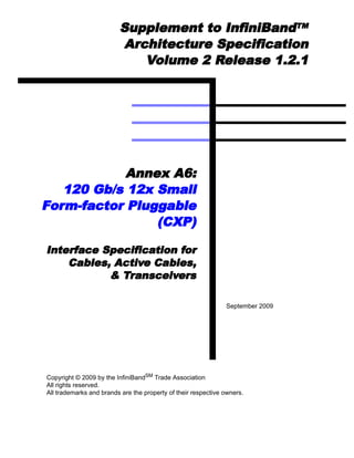
  • 1. Supplement to InfiniBandTM Architecture Specification Volume 2 Release 1.2.1 Annex A6: 120 Gb/s 12x Small Form-factor Pluggable (CXP) Interface Specification for Cables, Active Cables, & Transceivers September 2009 Copyright © 2009 by the InfiniBandSM Trade Association All rights reserved. All trademarks and brands are the property of their respective owners.
  • 2. InfiniBandTM Architecture - Annex A6 September 2009 VOLUME 2 - PHYSICAL SPECIFICATIONS FINAL RELEASE 1 Table 0 Revision History 2 Revision Date Revisions 3 1.0 9/18/2009 Released Version 4 5 6 7 LEGAL DISCLAIMER This specification provided “AS IS” and without any 8 warranty of any kind, including, without limitation, any express or implied warranty of non-infringement, 9 merchantability or fitness for a particular purpose. 10 In no event shall IBTA or any member of IBTA be liable 11 for any direct, indirect, special, exemplary, punitive, 12 or consequential damages, including, without limita- tion, lost profits, even if advised of the possibility of 13 such damages. 14 15 16 17 18 19 20 21 22 23 24 InfiniBandSM Trade Association Page 2 CXP Specification
  • 3. InfiniBandTM Architecture - Annex A6 September 2009 VOLUME 2 - PHYSICAL SPECIFICATIONS FINAL RELEASE TABLE OF CONTENTS 1 2 3 Chapter 1: Overview ..........................................................................................8 1.1 Design Targets and Compatibility ...............................................................................8 4 1.2 Participants ...............................................................................................................11 5 Chapter 2: Electrical Specification ................................................................12 6 2.1 Electrical Connector..................................................................................................12 2.2 Host board Schematic ..............................................................................................14 7 2.3 Low-Speed Electrical Contact/Signal Definitions ......................................................14 2.3.1 SDA, SCL ............................................................................................................. 14 8 2.3.2 Int_L/Reset_L ....................................................................................................... 14 9 2.3.3 PRSNT_L.............................................................................................................. 16 2.4 High-Speed Electrical Contact/Signal Definitions .....................................................16 10 2.4.1 Receive Signals: Rx[0-11][p/n].............................................................................. 16 2.4.2 Transmit Signals: Tx[0-11][p/n] ............................................................................. 17 11 2.5 Power Requirements ................................................................................................17 2.5.1 Host Power Supply Filtering.................................................................................. 17 12 2.5.2 Host Power Supply Specifications ........................................................................ 19 13 2.5.3 Power Budget Classes.......................................................................................... 19 2.6 ESD ..........................................................................................................................21 14 2.7 Hot Insertion and Removal .......................................................................................21 15 Chapter 3: High-Speed Electrical Signaling .................................................22 3.1 Introduction ...............................................................................................................22 16 3.2 Compliance Points ....................................................................................................22 17 3.3 Linear Passive / Linear Active Interface ...................................................................23 3.3.1 Host Differential Driver Outputs ............................................................................ 23 18 3.3.2 Compliant Channel - Module Tx Inputs to Module Rx Outputs............................. 23 3.3.3 Host Differential Receiver Inputs .......................................................................... 24 19 3.4 Limiting Active Interface............................................................................................25 20 3.4.1 Host Differential Driver Outputs ............................................................................ 25 3.4.2 CXP Module Tx Inputs .......................................................................................... 26 21 3.4.3 CXP Module Rx Outputs....................................................................................... 26 3.4.4 Host Differential Receiver Inputs .......................................................................... 27 22 23 24 InfiniBandSM Trade Association Page 3 CXP Specification
  • 4. InfiniBandTM Architecture - Annex A6 September 2009 VOLUME 2 - PHYSICAL SPECIFICATIONS FINAL RELEASE Chapter 4: Mechanical and Board Definition ................................................28 1 4.1 Introduction ...............................................................................................................28 4.2 CXP Datums and Component Alignment .................................................................29 2 4.3 CXP Module Package Dimensions ...........................................................................31 3 4.4 Connector Orientation Key........................................................................................36 4.5 Host PCB Footprint ...................................................................................................36 4 4.5.1 Grounding Pad Structure ...................................................................................... 38 4.5.2 Mating of CXP Module & Host PCBs to CXP Electrical Connectors.................... 38 5 4.6 Bezel for Systems Using CXP Transceivers.............................................................40 6 Chapter 5: Environmental and Thermal Specifications ..............................41 7 5.1 Physical and Mechanical Performance Requirements .............................................41 5.2 Connector Electrical Performance Requirements.....................................................42 8 5.3 Mechanical and Environmental Requirements .........................................................42 5.4 Thermal Performance Ranges..................................................................................43 9 5.5 CXP Housing Assembly Thermal Interfaces.............................................................44 10 5.6 EMI / Dust Cover for receptacle................................................................................49 11 Chapter 6: Cable Design .................................................................................50 6.1 Device, Module, and Cable Options .........................................................................50 12 6.1.1 Separable optical Transceiver .............................................................................. 50 6.1.2 Active optical Cable .............................................................................................. 51 13 6.1.3 Copper Cable........................................................................................................ 51 14 6.2 Latch Release ...........................................................................................................52 6.3 Cable Connectivity ....................................................................................................53 15 6.3.1 Cable Connectivity Mapping ................................................................................. 53 6.3.2 12x to 3-4x Cables ................................................................................................ 54 16 6.4 Lane Usage for 10-lane Interface .............................................................................55 17 6.5 Media-Specific Requirements - Optical Transceivers and Optical Cables ................56 6.5.1 Color Coding and Labeling of CXP Optical Transceivers ..................................... 56 18 6.5.2 Optical Connector Interfaces for 24-fiber transceivers.......................................... 57 6.5.3 Interface between 24-fiber connector and dual 12-fiber connectors..................... 58 19 Chapter 7: Management Interface ..................................................................59 20 7.1 Introduction ...............................................................................................................59 21 7.2 Voltage and Timing Specification ..............................................................................59 7.2.1 Management interface Voltage Specification ........................................................ 59 22 7.2.2 Management Interface Timing Specification ......................................................... 59 7.3 Memory Interaction Specifications ...........................................................................61 23 7.3.1 Timing for Memory Transactions........................................................................... 61 7.3.2 Timing for Control and Status Functions ............................................................... 62 24 InfiniBandSM Trade Association Page 4 CXP Specification
  • 5. InfiniBandTM Architecture - Annex A6 September 2009 VOLUME 2 - PHYSICAL SPECIFICATIONS FINAL RELEASE 7.3.3 Timing for Squelch and Disable Functions ........................................................... 63 1 7.4 Device Addressing and Operation ............................................................................64 7.5 Read/Write Functionality...........................................................................................65 2 7.5.1 CXP Memory Address Counter (Read AND Write Operations) ............................ 65 7.5.2 Read Operations (Current Address Read)............................................................ 66 3 7.5.3 Read Operations (Random Read) ........................................................................ 66 4 7.5.4 Read Operations (Sequential Read)..................................................................... 67 7.5.5 Write Operations (Byte Write) ............................................................................... 68 5 7.5.6 Write Operations (Sequential Write) ..................................................................... 69 7.5.7 Write Operations (Acknowledge Polling) .............................................................. 70 6 7.6 CXP Memory Map ....................................................................................................71 7.6.1 Tx Lower Page...................................................................................................... 73 7 7.6.2 Rx Lower Page ..................................................................................................... 79 8 7.6.3 Tx & Rx Common Upper Page 00h ...................................................................... 85 7.6.4 Tx Upper Page 01h............................................................................................... 91 9 7.6.5 Rx Upper Page 01h .............................................................................................. 92 10 11 12 13 14 15 16 17 18 19 20 21 22 23 24 InfiniBandSM Trade Association Page 5 CXP Specification
  • 6. InfiniBandTM Architecture - Annex A6 September 2009 VOLUME 2 - PHYSICAL SPECIFICATIONS FINAL RELEASE LIST OF FIGURES 1 2 3 Figure 1 CXP Conceptual Model ..................................................................................10 Figure 2 Example Host Board Schematic.....................................................................15 4 Figure 3 Recommended Host Board Power Supply Filtering .......................................18 Figure 4 Application Reference Model and Compliance Points ...................................23 5 Figure 5 General view, CXP Cable Connector & Housing Assembly, w/o heat sink ....28 Figure 6 Cable Connector and Receptacle Housing Datums .......................................30 6 Figure 7 Shielded Free (Plug) Integrated Cable Connector .........................................31 Figure 8 Shielded Free (Plug) Integrated Cable Connector, cont’d..............................32 7 Figure 9 Paddle Card Dimensions and Definition of Datums .......................................33 Figure 10 Fixed (Receptacle) Connector........................................................................34 8 Figure 11 Dimensions for Fixed (Receptacle) Connector in Figure 10...........................35 Figure 12 Connector Key................................................................................................36 9 Figure 13 Footprint - Shown in example application, Low Profile PCIe card..................37 Figure 14 Ground Pad - Shown in example application, Low Profile PCIe card ...........39 10 Figure 15 Panel Cutout - Shown in example application, Low Profile PCIe card ..........40 Figure 16 Receptacle Housing with Integrated Riding Heat Sink ...................................44 11 Figure 17 Heat Sink Interface on Connector Plug ..........................................................45 Figure 18 Heat Sink Thermal Interface Profile ...............................................................46 12 Figure 19 Heat Sink Clip Attach Points on Receptacle Housing ....................................47 Figure 20 Heat Sink Clip Structure .................................................................................48 13 Figure 21 EMI cover / Dust Cover ..................................................................................49 Figure 22 Optical Transceiver with separable optical cable ...........................................50 14 Figure 23 Active Optical Cable .......................................................................................51 Figure 24 Passive or Active Copper Cable.....................................................................51 15 Figure 25 Exemplary Latch Release Mechanism for a Cable Connector .......................52 Figure 26 12x to 3-4x cables ..........................................................................................54 16 Figure 27 Connector orientation for 24-fiber MPO/MTP connector ................................57 Figure 28 Connector interface between 24-fiber and Two 12-fiber connectors..............58 17 Figure 29 CXP 2-wire Serial Interface Timing Diagram..................................................60 Figure 30 CXP Device Addresses ..................................................................................65 18 Figure 31 Read Operation on Current Address ..............................................................66 Figure 32 Random Read ................................................................................................67 19 Figure 33 Sequential Address Read Starting at Current Address ..................................68 Figure 34 Sequential Address Read Starting with Random CXP Read .........................68 20 Figure 35 Write Byte Operation ......................................................................................69 Figure 36 Sequential Write Operation ............................................................................70 21 Figure 37 Memory Map 2-Wire Serial Addresses 1010 000x (Tx) & 1010 100x (Rx) ...72 22 23 24 InfiniBandSM Trade Association Page 6 CXP Specification
  • 7. InfiniBandTM Architecture - Annex A6 September 2009 VOLUME 2 - PHYSICAL SPECIFICATIONS FINAL RELEASE LIST OF TABLES 1 2 3 Table 0 Revision History ................................................................................................2 Table 1 Representative Transmission Media and Link Lengths .....................................9 4 Table 2 Contact Assignments for 12x Pluggable-CXP Interface ..................................13 Table 3 Power Supply Specification .............................................................................19 5 Table 4 Power Budget Classification............................................................................19 Table 5 Compliant Channel S Parameter Requirements for 10 Gb/s (QDR) ...............24 6 Table 6 Driver Characteristics for 10 Gb/s, for Limiting Active interfaces ....................25 Table 7 CXP Limiting Active Module Tx Input Characteristics for 10 Gb/s ..................26 7 Table 8 CXP Limiting Active Module Rx Output Characteristics for 10 Gb/s ...............26 8 Table 9 Receiver Characteristics for 10 Gb/s...............................................................27 Table 10 Definition of Datums ........................................................................................29 9 Table 11 Module & Receptacle Connector Physical Requirements ...............................41 Table 12 Recommended Connector Physical Parameters ............................................41 10 Table 13 Module & Receptacle Connector Electrical Performance Requirements ........42 Table 14 Module and Receptacle Mechanical and Environmental Requirements .........43 11 Table 15 Temperature Classification of Module Case....................................................44 Table 16 Cable Connector Signal Assignment...............................................................53 12 Table 17 12x Board Connector Signal Assignment for 12x to 3-4x Cables ...................55 Table 18 Low Speed Control and Sense Signal Specifications......................................59 13 Table 19 CXP 2-Wire Serial Interface Timing Specifications..........................................60 Table 20 CXP Memory Transaction Timing Specification...............................................61 14 Table 21 I/O Timing for Control and Status Functions....................................................62 15 Table 22 I/O Timing for Squelch and Disable.................................................................63 Table 23 Tx Lower Page Memory Map ..........................................................................73 16 Table 24 Rx Lower Page Memory Map (Optional) .........................................................79 Table 25 Tx & Rx Upper Page 00h Memory Map ..........................................................85 17 Table 26 Tx Upper Page 01h Memory Map ...................................................................91 Table 27 Rx Upper Page 01h Memory Map ...................................................................92 18 19 20 21 22 23 24 InfiniBandSM Trade Association Page 7 CXP Specification
  • 8. InfiniBandTM Architecture - Annex A6 Overview September 2009 VOLUME 2 - PHYSICAL SPECIFICATIONS FINAL RELEASE CHAPTER 1: OVERVIEW 1 2 3 This specification is a description of a 12x form-factor pluggable active de- vice interface, with 12 transmit and 12 receive lanes, capable of sup- 4 porting bit-rates in excess of 10 Gb/s per lane on a variety of electrical and optical transmission technologies. 5 This specification describes the form factor, electrical, mechanical, power, 6 and thermal interfaces between the devices or cables and the systems. The transmission technology (e.g., optical or electronic), transmission 7 medium (e.g., single-mode, multi-mode fiber, or copper), form factor (i.e., with cable attached to the pluggable device, or detachable with a sepa- 8 rable connector), and physical layer definition for the communication be- tween transceivers are not explicitly specified. However, the 9 specifications are intended to support several different technologies, in- cluding VCSEL/MMF parallel ribbon fiber links. 10 The current primary target for this technology is the InfiniBand architec- 11 ture, at the 12x-QDR (Quad Data Rate) rate, as well as DDR and SDR rates. Other standards, such as Ethernet at the 100 Gb/s data rate and 12 Fibre Channel, may be supported as well.1 13 1.1 DESIGN TARGETS AND COMPATIBILITY 14 This paragraph describes the design targets of the device. These targets are used as foundation for making decisions regarding the design of the 15 interface and related devices. 16 • Transmission Bandwidth: The interface should be capable of comfort- ably supporting data communications at up to 10.5 Gb/s on each of 17 12 lanes, in order to support at least the following link options. • 12x QDR InfiniBand links, operating at (12+12)x10.0 Gb/s. 18 • 100 Gb/s Ethernet, using a 10-lane PHY and a 64b/66b line code (e.g., 10.3125 using 64b/66b on 10 lanes), as defined by the 19 IEEE. 20 • Electrical Interface Compatibility: Low-speed signals should be com- patible with electrical interface specifications of Section 2.3 on page 21 14, high-speed signals should be compatible with InfiniBand QDR 22 1. Terminology note: The name CXP is intended to derive from several sources: C = the Roman numeral for 100, indicating a form-factor targeted for >100 23 Gb/s per direction transmission. C is also the hexadecimal character for 12, indicating an interface with 12 lanes per direction. XP = eXtended-capability Pluggable form-factor. 24 InfiniBandSM Trade Association Page 8 CXP Specification
  • 9. InfiniBandTM Architecture - Annex A6 Overview September 2009 VOLUME 2 - PHYSICAL SPECIFICATIONS FINAL RELEASE electrical interface specifications defined in the InfiniBand Specifica- 1 tion, Vol. 2, Chapter 6, as extended or modified in Chapter 3: High- Speed Electrical Signaling of this annex. 2 • Transmission Media Compatibility: This interface is expected to sup- port modules or cables of at least the following types: 3 • Copper Cable, un-equalized or passively equalized, 4 • Active Copper Cable with receive-side active equalization, • Active Copper Cable with active equalization on both transmit 5 and receive sides, • Active Optical Cable Assembly, and 6 • Separable Optical Transceiver and fiber optic cable. 7 This variety of transmission technologies allow cost-effective imple- mentation across a wide range of link lengths using the same host re- 8 ceptacle and electrical interfaces. Example representative link lengths are shown in Table 1 on page 9. Note that these link lengths are not 9 precise, and are not intended to be normative. 10 Table 1 Representative Transmission Media and Link Lengths 11 Transmission Speed Transmission Medium 12 QDR DDR SDR 10.0 Gb/s 5.0 Gb/s 2.5 Gb/s 13 Copper Cable, un-equalized or ~6-8 m ~9-12 m 12-15 m passively equalized 14 Active Copper, Rx-side active 9-12 m 8-20 m 12-18 m 15 Active Copper, Both sides active 14-20 m 20-30 m 30-50 m 16 Active Optical Cable Assembly ~100 - 300 m 100-300 m 100-300 m 17 Optical Transceiver Up to ~10 km Up to ~10 km Up to ~10 km 18 Note also that explicit transmission technology choices within an ac- 19 tive cable assembly (e.g., single-mode vs. multi-mode optical trans- mission, glass vs. plastic optical fiber, or equalization and coding 20 techniques) are not addressed by this specification. This document specifies the electrical, mechanical and thermal interfaces between 21 “module” (cable plug, or transceiver) and the host. Any transmission technology which transports data transmission between two inter- 22 faces at the specified speed with good signal integrity at each end is compliant. 23 24 InfiniBandSM Trade Association Page 9 CXP Specification
  • 10. InfiniBandTM Architecture - Annex A6 Overview September 2009 VOLUME 2 - PHYSICAL SPECIFICATIONS FINAL RELEASE Figure 1 on page 10 illustrates the CXP conceptual model, with a 1 single host interface receptacle supporting a variety of transmission technologies, cost-effectively supporting a variety of link lengths. 2 3 4 5 6 7 8 9 10 11 12 13 14 15 16 17 18 19 20 Figure 1 CXP Conceptual Model 21 22 23 24 InfiniBandSM Trade Association Page 10 CXP Specification
  • 11. InfiniBandTM Architecture - Annex A6 Overview September 2009 VOLUME 2 - PHYSICAL SPECIFICATIONS FINAL RELEASE 1.2 PARTICIPANTS 1 The following individual served as editor of this annex during its creation: 2 Alan Benner 3 4 The following individuals provided active contributions to this annex during its creation: 5 Ed Bright Jay Neer 6 Rupert Dance Vit Novak 7 8 Matt Davis Tom Palkert 9 Jay Diepenbrock John Petrilla 10 Chris Diminico Michael Rost 11 Robert Elliot Zuowei Shen 12 Jason Ellison Harel Shvarzberg 13 Frank Flens Wei Tang 14 Galen Fromm Ola Torudbakken 15 Keith Lang Dean Wallace 16 Ofer Levi Michael Walmsley 17 Jim McGrath 18 19 20 21 22 23 24 InfiniBandSM Trade Association Page 11 CXP Specification
  • 12. InfiniBandTM Architecture - Annex A6 Electrical Specification September 2009 VOLUME 2 - PHYSICAL SPECIFICATIONS FINAL RELEASE CHAPTER 2: ELECTRICAL SPECIFICATION 1 2 3 This chapter contains contact definitions for the CXP transceiver. Compli- ance points for high-speed signal electrical measurements are defined in 4 Figure 4 on page 23. Compliance points for all other electrical signals are at comparable points at the host edge card connector. 5 2.1 ELECTRICAL CONNECTOR 6 Table 2 on page 13 shows the signal symbols and contact numbering for the CXP module edge connectors. The diagram shows the module PCB 7 edge as a top and bottom view, for both circuit cards in the two-level con- nector. There are 21 pads per level, for a total of 84, with 48 pads allocated 8 for (12+12) differential pairs, 28 for Signal Common or Ground (GND), 4 for power connections, 4 for control/service. Mapping of these contacts 9 into physical locations in the device connector and the receptacle are shown in Figure 8 on page 32, and Figure 10 on page 34, respectively. 10 The operation of the low-speed control and status lines (PRSNT_L, 11 Int_L/Reset_L, SCL, & SDA) is described in Section 2.3, “Low-Speed Electrical Contact/Signal Definitions,” on page 14, and operation of the 12 high-speed lines for receiving and transmitting data is described in Section 2.4, “High-Speed Electrical Contact/Signal Definitions,” on 13 page 16. 14 15 16 17 18 19 20 21 22 23 24 InfiniBandSM Trade Association Page 12 CXP Specification
  • 13. InfiniBandTM Architecture - Annex A6 Electrical Specification September 2009 VOLUME 2 - PHYSICAL SPECIFICATIONS FINAL RELEASE Table 2 Contact Assignments for 12x Pluggable-CXP Interface 1 Bottom side Top Side Contact Contact 2 I/O # Name Name I/O # Length Length Receiver -- Top Card 3 C1 GND GND D1 C2 Rx1p Rx0p D2 4 C3 Rx1n Rx0n D3 C4 GND GND D4 5 C5 Rx3p Rx2p D5 C6 Rx3n Rx2n D6 6 C7 GND GND D7 C8 Rx5p Rx4p D8 Card Edge 7 C9 Rx5n Rx4n D9 C10 GND GND D10 8 C11 Rx7p Rx6p D11 C12 Rx7n Rx6n D12 C13 GND GND D13 9 C14 Rx9p Rx8p D14 C15 Rx9n Rx8n D15 10 C16 GND GND D16 C17 Rx11p Rx10p D17 11 C18 Rx11n Rx10n D18 C19 GND GND D19 12 C20 PRSNT_L Vcc3.3-Rx D20 C21 Int_L/Reset_L Vcc12-Rx D21 13 Transmitter -- Bottom Card A1 GND GND B1 14 A2 Tx1p Tx0p B2 A3 Tx1n Tx0n B3 15 A4 GND GND B4 A5 Tx3p Tx2p B5 16 A6 Tx3n Tx2n B6 A7 GND GND B7 A8 Tx5p Tx4p B8 17 Card Edge A9 Tx5n Tx4n B9 A10 GND GND B10 18 A11 Tx7p Tx6p B11 A12 Tx7n Tx6n B12 19 A13 GND GND B13 A14 Tx9p Tx8p B14 20 A15 Tx9n Tx8n B15 A16 GND GND B16 21 A17 Tx11p Tx10p B17 A18 Tx11n Tx10n B18 22 A19 GND GND B19 A20 SCL Vcc3.3-Tx B20 A21 SDA Vcc12-Tx B21 23 24 InfiniBandSM Trade Association Page 13 CXP Specification
  • 14. InfiniBandTM Architecture - Annex A6 Electrical Specification September 2009 VOLUME 2 - PHYSICAL SPECIFICATIONS FINAL RELEASE 2.2 HOST BOARD SCHEMATIC 1 Figure 2 on page 15 shows an example of a host board schematic for CXP, with connections to host SerDes and control logic. For EMI protec- 2 tion the signals to the connector should be shut off when the CXP trans- ceiver is removed. Standard board layout practices such as connections 3 to Vcc3.3 and Vcc12 and GND with vias, use of short and equal-length dif- ferential signal lines, use of microstrip-lines, and 50Ω /100Ω terminations 4 are recommended. The chassis ground (case common) of the CXP module should be isolated from the module’s circuit ground, GND. 5 Note that AC coupling capacitors on the high-speed signals are imple- 6 mented inside the device or cable. This is opposite to the configuration de- scribed in InfiniBand Architecture Specification, Volume 2, Compliance 7 Statement C6-8.2.1, which specifies that DC blocking capacitors shall not be mounted inside the cable assembly for cables using MicroGiga-CN 8 connectors. 9 2.3 LOW-SPEED ELECTRICAL CONTACT/SIGNAL DEFINITIONS 2.3.1 SDA, SCL 10 SCL is the clock of the two-wire serial interface, and SDA is the data for 11 the 2-wire serial interface. Operation of this interface is described in detail in Chapter 7: Management Interface, SCL and SDA must be pulled up in 12 the host, through an pull-up resistor of value appropriate to the overall bus capacitance and the rise and fall time requirements listed in Table 19 on 13 page 60. 14 2.3.2 INT_L/RESET_L Int_L/Reset_L is a bidirectional signal. When driven from the host, it oper- 15 ates logically as a Reset signal. When driven from the module, it operates logically as an Interrupt signal. In both cases, the signal is asserted low, 16 as indicated by the ’_L’ suffix. The Int_L/Reset_L signal requires open col- lector outputs in both the host and module, and must be pulled up on the 17 host board, as described for SDA and SCL. Int_L and Reset_L indications are distinguished from each other by timing - a shorter assertion, driven 18 by the module, indicates an interrupt, and a longer assertion of the signal, driven by the host, indicates a reset, as listed in Table 21 on page 62. 19 Int_L operation: When Int_L/Reset_L is pulled “Low” by the module for 20 longer than the minimum interrupt pulse width (tInt_L,PW-min) and shorter than the maximum interrupt pulse width (tInt_L,PW-max) the signal signifies 21 an interrupt. An interrupt indicates a possible module operational fault or a module status critical to the host system. The host identifies the cause 22 of the interrupt using the 2-wire serial interface. Int_L must operate in pulse mode (vs. static mode), in order to distinguish a short interrupt 23 signal from a longer reset signal, so the module must de-assert Int_L/Reset_L after the interrupt has been signaled. 24 InfiniBandSM Trade Association Page 14 CXP Specification
  • 15. InfiniBandTM Architecture - Annex A6 Electrical Specification September 2009 VOLUME 2 - PHYSICAL SPECIFICATIONS FINAL RELEASE 1 Pullup Voltage CXP Module 2 Vcc3.3_Rx 1.5κ Ω − 10κΩ Vcc12_Rx Vcc3.3_Tx Power Conversion 3 1.5κ Ω − 10κΩ 1.5κ Ω − 10κΩ >51κΩ Vcc12_Tx & Distribution Int_L/Reset_L 4 Svc. Proc. / SCL Microcontroller PLD/PAL SDA or EEPROM 5 PRSNT_L <5.2κ Ω 6 GND Tx Disable <0:11> Tx Fault <0:11> 7 Rx Rate <0:11> Rx LOS <0:11> 100 Ω 0.1 uF 0.1 uF GND Receive 100 Ω 0.1 uF 0.1 uF Circuitry 8 Signal 100 Ω 0.1 uF 0.1 uF Common 100 Ω 0.1 uF 0.1 uF 9 100 Ω 0.1 uF 0.1 uF 100 Ω 0.1 uF 0.1 uF 10 100 Ω 0.1 uF 0.1 uF Protocol Logic 100 Ω 0.1 uF 0.1 uF 11 Rx Data Bus 100 Ω 0.1 uF 0.1 uF 12 100 Ω 0.1 uF 0.1 uF 100 Ω 0.1 uF 0.1 uF 13 100 Ω 0.1 uF 0.1 uF 12x 14 0.1 uF 0.1 uF 100 Ω SerDes Transmit 100 Ω 0.1 uF 0.1 uF Circuitry 15 Tx Data Bus 0.1 uF 0.1 uF 100 Ω 0.1 uF 0.1 uF 100 Ω 16 0.1 uF 0.1 uF 100 Ω 0.1 uF 0.1 uF 100 Ω 17 Note: Protocol Logic and SerDes may be 0.1 uF 0.1 uF 100 Ω on the same chip, or on different chips 18 0.1 uF 0.1 uF 100 Ω 0.1 uF 0.1 uF 100 Ω 0.1 uF 0.1 uF 100 Ω 19 0.1 uF 0.1 uF 100 Ω 20 0.1 uF 0.1 uF 100 Ω Case Ground Note: A Passive Copper cable would need 21 only one decoupling capacitor per lane, and would not have internal termination. 22 23 Figure 2 Example Host Board Schematic 24 InfiniBandSM Trade Association Page 15 CXP Specification
  • 16. InfiniBandTM Architecture - Annex A6 Electrical Specification September 2009 VOLUME 2 - PHYSICAL SPECIFICATIONS FINAL RELEASE Reset_L operation: When the Int_L/Reset_L signal is pulled “Low” by the 1 host for longer than the minimum reset pulse length (treset_L,PW-min), it ini- tiates a complete module reset, returning all user module settings to their 2 default state. There is no maximum reset pulse length. Module Reset As- sert Time (t_init) starts on the rising edge after the low level on the 3 Reset_L signal is released. During the execution of a reset (t_init) the host shall disregard all status bits until the module indicates a completion 4 of the reset interrupt. The module indicates this by posting an Int_L signal with the Data_Not_Ready bit (Memory Map, Byte 2, bit 0) negated (set to 5 0). Note that on power up (including hot insertion) the module should post this completion of reset interrupt without requiring a reset from the host. 6 2.3.3 PRSNT_L 7 PRSNT_L is used to indicate when the module is plugged into the host receptacle. PRSNT_L is pulled up to Vcc3.3 on the host board through 8 >50 kOhm. It is pulled down to signal common through 5.2 kOhm in mod- ules requiring 12V power, and tied directly down to signal common (no re- 9 sistor) in modules requiring 3.3V power only. The PRSNT_L signal is asserted “Low” when inserted and deasserted “High” when the module is 10 physically absent from the host connector. 11 2.4 HIGH-SPEED ELECTRICAL CONTACT/SIGNAL DEFINITIONS 12 2.4.1 RECEIVE SIGNALS: RX[0-11][P/N] Rx[0-11][p/n] are CXP module receiver data outputs. They are AC-cou- 13 pled differential lines that should be terminated with 100 Ohm differential at the Host ASIC or SerDes. The AC coupling is inside the CXP module 14 and not required on the Host board. 15 Output squelch for loss of input signal (Rx Squelch), is an optional func- tion. Where implemented it shall function as follows. In the event of the op- 16 tical or electrical signal on any physical lane becoming equal to or less than the level required to assert loss of signals (Rx LOS), then the receiver 17 data output for that lane shall be squelched or disabled. In the squelched or disabled state, output impedance levels are maintained while the differ- 18 ential voltage swing shall be less than 50 mVpp, This voltage swing limit provides margin vs. the value specified for VRSD, Signal Threshold for re- 19 ceiver signal detection (85 mVpp in Rel. 1.2.1) in InfiniBand Architecture Specification, Volume 2, Chapter 6: High Speed Electrical Signaling - 2.5, 20 5.0, & 10.0 Gb/s 21 In normal operation, where Rx Squelch is implemented, the default case has Rx Squelch active. Rx Squelch can be deactivated using Rx Squelch 22 Disable through the 2-wire serial interface. Rx Squelch Disable is an op- tional function. 23 24 InfiniBandSM Trade Association Page 16 CXP Specification
  • 17. InfiniBandTM Architecture - Annex A6 Electrical Specification September 2009 VOLUME 2 - PHYSICAL SPECIFICATIONS FINAL RELEASE 2.4.2 TRANSMIT SIGNALS: TX[0-11][P/N] 1 Tx[0-11][p/n] are CXP module transmitter data inputs. They are AC-cou- pled differential lines with 100 Ohm differential terminations inside the 2 CXP module. The AC coupling is inside the CXP module and not required on the Host board. 3 Output squelch (Tx Squelch), for loss of input signal, (Tx LOS), is an op- 4 tional function. Where implemented it shall function as follows. In the event of the differential, peak-to-peak electrical signal on any lane be- 5 comes equal to or less than 50 mVpp, then the transmitter optical output for that lane shall be squelched and the associated Tx LOS flag set. For 6 an optical transceiver with separable optical connector, the optical modu- lation amplitude (OMA) when squelched shall be less than or equal to -26 7 dBm. 8 In normal operation, where Tx Squelch is implemented, the default case has Tx Squelch active. Tx Squelch can be deactivated using Tx Squelch 9 Disable through the 2-wire serial interface. Tx Squelch Disable is an op- tional function. 10 2.5 POWER REQUIREMENTS 11 Power for the module is supplied through 4 contacts: Vcc3.3-Rx, Vcc12- Rx, Vcc3.3-Tx and Vcc12-Tx. Power is applied concurrently to them. 12 Since different classes of modules exist with pre-defined maximum power 13 consumption limits, it is necessary to avoid exceeding the system power supply limits and cooling capacity when a module is inserted into a system 14 designed to only accommodate lower power modules. It is recommended that the host, through the management interface, identify the power con- 15 sumption class of the module before allowing the module to go into high power mode. 16 A host board together with the CXP module(s) forms an integrated power 17 system. The host supplies stable power to the module. The module limits electrical noise coupled back into the host system and limits inrush 18 charge/current during hot plug insertion. 19 All specifications shall be met at the maximum power supply current. No power sequencing of the power supply is required of the host system 20 since the module sequences the contacts in the order of ground, supply and signals during insertion. 21 2.5.1 HOST POWER SUPPLY FILTERING 22 The host board should use the power supply filtering network shown in 23 Figure 3 on page 18, or an equivalent. Any voltage drop across a filter net- work on the host is counted against the host DC set point accuracy spec- 24 InfiniBandSM Trade Association Page 17 CXP Specification
  • 18. InfiniBandTM Architecture - Annex A6 Electrical Specification September 2009 VOLUME 2 - PHYSICAL SPECIFICATIONS FINAL RELEASE ification. Inductors with DC Resistance of less than 0.1 Ω should be used 1 in order to maintain the required voltage at the Host Edge Card Connector. 2 3 1 uH CXP Module 4 Vcc3.3-Rx 5 6 Vcc_host = 3.3 V 10 uF 0.1 uF GND 7 1 uH 8 Vcc3.3-Tx 9 10 uF 0.1 uF 10 uF 0.1 uF GND 10 11 1 uH Vcc12-Rx 12 10 uF 0.1 uF 13 Vcc_host = 12 V GND 14 1 uH 15 Vcc12-Tx 10 uF 0.1 uF 10 uF 0.1 uF 16 GND 17 18 19 Figure 3 Recommended Host Board Power Supply Filtering 20 21 22 23 24 InfiniBandSM Trade Association Page 18 CXP Specification