SlideShare uma empresa Scribd logo
Atomic Layer Deposition solutions
for SiC Power Electronics
Integrated ALD passivation/gate dielectric
stack for SiC MOSFET
Mikko Söderlund – Semiconductor Business Unit
April 19, 2023
17.4.2023 – CONFIDENTIAL
Company Introduction and More-than-Moore market focus
Semiconductor ALD solutions and materials for SiC power devices
Inflection in passivation/gate dielectric
Introduction to ALD equipment
Differentiated Beneq Transform® ALD cluster tool
Outline
17.4.2023 – CONFIDENTIAL
Semiconductor ALD products
Beneq Transform® and C2
for the up to 200 mm MtM market
Beneq Transform® 300 & C3
for the 300 mm MtM market
Beneq Prodigy™
for Compound Semi
and MEMS markets
200 mm and smaller wafers 300 mm wafers
Prodigy™ Transform®
Transform® Lite Transform® 300
17.4.2023
Semiconductor Markets we serve
Power devices
Image sensors
R&D
µOLED
Advanced packaging
RF Ics, Filters
More-than-Moore device fabrication:
✓ Power devices
✓ RF Filter devices
✓ RF ICs
✓ CMOS image sensors
✓ µOLED
✓ LED, µLED, EEL, VCSEL, detectors and Si photonics
✓ MEMS, sensors and actuators
✓ Advanced Packaging (TSV, CSP)
✓ Smart Power
✓ Microcontroller and e-NVM
✓ RF, Analog and mixed signal
17.4.2023 – CONFIDENTIAL
300 mm
*
This presentation
17.4.2023 – CONFIDENTIAL
BENEQ ALD Solutions for Power Devices
Market
segments
Gate Dielectric
(SiO2, High-k)
Surface
passivation
Nucleation &
seed, doping
Metal & TCO Final Passivation
(moisture
barrier)
Trench MOSFET
✓ ✓ ✓
SJ MOSFET
✓ ✓ ✓
IGBT
✓ ✓ ✓
SiC MOSFET &
Trench MOSFET ✓ ✓ ✓ ✓
GaN HEMT
✓ ✓ ✓ ✓ ✓
Vertical GaN
✓ ✓ ✓ ✓
Plasma enhanced single wafer and/or sequential PEALD + thermal batch processing
17/04/2023
SiC Market Drivers
Beneq
Confidential
17.4.2023 – CONFIDENTIAL
SiC market drivers - devices and modules
• 800 V battery systems enable fast charging and accelerate penetration of SiC devices and modules in BEV
courtesy to their advantage over Si IGBT i.e. higher performance gain per unit cost for 1200 V SiC.
• 1200 V SiC devices, in hybrid and full SiC modules, are supporting the raise of renewable energy capacity.
2021 device market 2021-2027 CAGR
685 M$ 39 %
37 M$ 24 %
145 M$ 19 %
78 M$ 16 %
Power SiC 2022 |
www.yole.fr|
©2022
17.4.2023 – CONFIDENTIAL
SiC Power devices market forecast and market share
• The SiC device market is expected to reach $6.1B by 2027. SiC has strongly penetrated the automotive market,
which will represent more than 75% of the total SiC device market in 2027.
• Despite the pandemic and semiconductor shortage in the past 2 years, SiC ramp ups are ongoing. EV/HEV is
taking off, along with the transition from 400V to 800V battery systems.
• The global SiC device market grew 57% in 2020-2021. Some major device suppliers performed at such rate.
Power SiC 2022 |
www.yole.fr|
©2022
17.4.2023 – CONFIDENTIAL
Power SiC 2022 |
www.yole.fr|
©2022
SiC MOSFET product development
• Since market launch of SiC MOSFET early 2021, device manufacturers have released multiple generations of
devices to support qualification in various applications.
• Driven by lower ON resistance and smaller devices, Trench SiC MOSFET R&D started about 10 years ago.
17/04/2023
ALD inflection for SiC MOSFET
Beneq
Confidential
17.4.2023 – CONFIDENTIAL
BENEQ ALD roadmap for SiC MOSFET
T. Kimoto, Performance Improvement and Reliability Physics in SiC MOSFETs,
IRPS 2022, Kyoto University
Nitridation anneal post thermal oxidation
Power SiC 2022 |
www.yole.fr|
©2022
Reduced Ron
Conformality
&
film quality BENEQ ALD roadmap
Thermal ALD SiO2 w. anneal
Plasma / thermal ALD SiO2 w. anneal
Interface preclean and nitridation
w. reduced anneal
Introduce High k to replace SiO2
for higher reliability
Materials & process solutions for SiC MOSFET
17.4.2023 – CONFIDENTIAL
✓ Optional** PEALD Nitride interfacial layer (AlN or Si3N4)
• Further passivation of the SiC surface by nitridation
• Effectively blocks oxygen to the SiC surface, leading to reduced Dit
✓ Deposition of gate dielectric (SiO2, High-k or SiO2/High-k)
• Provide necessary performance as gate dielectric
• High-k to improve reliability of the gate dielectric
• Al2O3 or SiO2 acts as a capping material to prevent oxidation of the surface
✓ In-situ* plasma preclean to remove surface damage and/or provide surface
nitridation of the surface
• Remove cristal disorder at the surface SiC, Carbon clusters, caused by oxidation of SiC
• Nitridation for passivation of SiC surface
• Provide high quality interface for low density of interface states
T. Kimoto et al. IEDM 2021
* In-situ to the PEALD process module
** alternative to NO Anneal
Transform® Batch ALD performance – SiO2
Performance Value
Breakdown (MV/cm) > 9.5
Leakage current density, @
5 MV/cm (A/cm2)
~ 1 x 10⁻⁸
Refractive index @ 633 nm 1.45
Density (g/cm3) 2
Current vs. Electric Field
Process temperature 300°C
Wafer size 200mm
WiW: ~ 0.6%, 1σ
Wt: ~ 0.2%, 1σ
BtB: ~ 0.26%, 1σ
Throughput: 12 WPH @50 nm
Pre-clean/treat and PEALD SiN is available on the single wafer plasma module
17.4.2023 – CONFIDENTIAL
25-wafer batch
ToF-ERDA profile of thermal SiO2
As deposited thermal SiO2
O: 61.0 ± 0.6 at-%
Si: 29.6 ± 0.5 at-%
H: 9.4 ± 0.6 at-%
C: <0.2 at-%
(As deposited PEALD SiO2)
O: 62.8 ± 0.6 at-%
Si: 31.3 ± 0.5 at-%
H: 5.8 ± 0.5 at-%
C: <0.2 at-%
SiO2 ALD / anneal integration - current status
17.4.2023 – CONFIDENTIAL
Before annealing After annealing
• Low hysteresis and fixed charges are obtained after anneal for both thermal and plasma ALD SiO2
• Plasma ALD SiO2 better control of the interface/trapped charges and will benefit of in-situ plasma pre-clean technology
17/04/2023
Beneq ALD equipment
for the Wafer Fabs
Beneq
Confidential
17/04/2023
• Highly versatile cluster platform supporting a wide
range of material and applications
• Breakthrough in throughput with pre-heating and
flow optimized mini-batch reactor design
• Differentiated & patented sequential ALD processing
combining plasma enhanced and thermal batch ALD
for “best of both” worlds capability
• Beneq Transform has become 1st choice for Tier1
IDM’s, Foundries and RTOs in Power, RF,
MicroLED/Photonics, CIS, MEMS and Advanced
Packaging
Introducing Beneq Transform ®
Beneq
Confidential
Versatile platform dedicated to More-than-Moore device fabrication
Beneq Transform is your engine for the SiC materials revolution!
17/04/2023
Beneq Transform© enables sequential processing
For best-of-both-worlds plasma enhanced and thermal ALD processing capability
2
Pre-heating module
✓ Productivity booster, > 40 % higher WPH
✓ Remove/outgas trace water and organics
2
3
Plasma-enhanced ALD process module
✓ Flexible single-wafer plasma chamber, direct or remote CCP type
✓ In-situ plasma pre-treatment/surface activation for reduced Dit
✓ For deposition of thin (e.g. 3-5 nm SiO2, AlN, SiN) interfacial layer (IL)
3
4
Thermal batch process module
✓ Receives wafers after SW PEALD process
without air-break (in-vacuum transfer)
✓ Up to 25 wafer batch size
✓ For deposition of thicker dielectric layers e.g.
50-100 nm SiO2, or high-k Al2O3, HfO2….
4
1
Load-lock
✓ Two load-locks, each for 25 wafer lot size
1
1
5
Cooling module
✓ For rapid cooling of wafers to < 60 C
5
3rd retrofit process module
✓ For example, 2nd PEALD chamber for
additional capacity
✓ Or additional process capability such as
Schottky contact, Final passivation, …
High (double-digit ) WPH reached for pre-clean/IL/dielectric stack
Beneq
Confidential
to customers’ developing needs.
Add value
as a caring community.
Make it together
continuously and step by step.
Keep improving
encouraging others to learn, too.
Stay curious
To fulfill our mission, we:
www.beneq.com |
info@beneq.com | +358 9 7599 530
mikko.soderlund@beneq.com
Beneq is the home of atomic layer
deposition. In 1984, we established the
world’s first industrial production using
ALD. Today, we lead the market with
products for R&D (TFS 200, TFS 500, R2),
semiconductor device fabrication
(Transform®, Transform® 300, and
ProdigyTM), 3D and batch production
(P400A, P800, P1500), ultra-fast spatial
ALD (C2R), and roll-to-roll ALD (Genesis).

Mais conteúdo relacionado

Mais procurados

Er-doped hybrid waveguide amplifiers with multiple spatially engineered activ...
Er-doped hybrid waveguide amplifiers with multiple spatially engineered activ...Er-doped hybrid waveguide amplifiers with multiple spatially engineered activ...
Er-doped hybrid waveguide amplifiers with multiple spatially engineered activ...Beneq
 
2.5D / 3D TSV & Wafer-Level Stacking: Technology & Market Updates 2019 Report...
2.5D / 3D TSV & Wafer-Level Stacking: Technology & Market Updates 2019 Report...2.5D / 3D TSV & Wafer-Level Stacking: Technology & Market Updates 2019 Report...
2.5D / 3D TSV & Wafer-Level Stacking: Technology & Market Updates 2019 Report...Yole Developpement
 
Rotary PEALD: in-situ monitoring of optical coatings
Rotary PEALD: in-situ monitoring of optical coatingsRotary PEALD: in-situ monitoring of optical coatings
Rotary PEALD: in-situ monitoring of optical coatingsBeneq
 
Film Properties of ALD SiNx Deposited by Trisilylamine and N2 Plasma
Film Properties of ALD SiNx Deposited by Trisilylamine and N2 PlasmaFilm Properties of ALD SiNx Deposited by Trisilylamine and N2 Plasma
Film Properties of ALD SiNx Deposited by Trisilylamine and N2 PlasmaBeneq
 
Roll-to-Roll ALD Coatings for Battery Cell Interfaces at Production Scale
Roll-to-Roll ALD Coatings for Battery Cell Interfaces at Production ScaleRoll-to-Roll ALD Coatings for Battery Cell Interfaces at Production Scale
Roll-to-Roll ALD Coatings for Battery Cell Interfaces at Production ScaleBeneq
 
GaAs Wafer and Epiwafer Market: RF, Photonics, LED, Display and PV Applicatio...
GaAs Wafer and Epiwafer Market: RF, Photonics, LED, Display and PV Applicatio...GaAs Wafer and Epiwafer Market: RF, Photonics, LED, Display and PV Applicatio...
GaAs Wafer and Epiwafer Market: RF, Photonics, LED, Display and PV Applicatio...Yole Developpement
 
Advanced Substrates Overview: From IC Package to Board - 2017 Report by Yole ...
Advanced Substrates Overview: From IC Package to Board - 2017 Report by Yole ...Advanced Substrates Overview: From IC Package to Board - 2017 Report by Yole ...
Advanced Substrates Overview: From IC Package to Board - 2017 Report by Yole ...Yole Developpement
 
Fab presentaion
Fab presentaionFab presentaion
Fab presentaionsamiseecs
 
Status of Advanced Substrates 2019 report by Yole Développement
Status of Advanced Substrates 2019 report by Yole DéveloppementStatus of Advanced Substrates 2019 report by Yole Développement
Status of Advanced Substrates 2019 report by Yole DéveloppementYole Developpement
 
Fan-Out and Embedded Die: Technologies & Market Trends 2015 Report by Yole De...
Fan-Out and Embedded Die: Technologies & Market Trends 2015 Report by Yole De...Fan-Out and Embedded Die: Technologies & Market Trends 2015 Report by Yole De...
Fan-Out and Embedded Die: Technologies & Market Trends 2015 Report by Yole De...Yole Developpement
 
Bonding and Lithography Equipment Market for More than Moore Devices by Yole ...
Bonding and Lithography Equipment Market for More than Moore Devices by Yole ...Bonding and Lithography Equipment Market for More than Moore Devices by Yole ...
Bonding and Lithography Equipment Market for More than Moore Devices by Yole ...Yole Developpement
 
Fan-Out Packaging: Technologies and Market Trends 2019 report by Yole Dévelop...
Fan-Out Packaging: Technologies and Market Trends 2019 report by Yole Dévelop...Fan-Out Packaging: Technologies and Market Trends 2019 report by Yole Dévelop...
Fan-Out Packaging: Technologies and Market Trends 2019 report by Yole Dévelop...Yole Developpement
 
Atomic Layer Deposition: a process technology for transparent conducting oxides
Atomic Layer Deposition: a process technology for transparent conducting oxidesAtomic Layer Deposition: a process technology for transparent conducting oxides
Atomic Layer Deposition: a process technology for transparent conducting oxidescdtpv
 
ALD for semiconductor applications_Workshop2010
ALD for semiconductor applications_Workshop2010ALD for semiconductor applications_Workshop2010
ALD for semiconductor applications_Workshop2010Gabriela Dilliway
 
Nano-Imprint Technology Trends for Semiconductor Applications 2019 Report by...
Nano-Imprint Technology Trends for Semiconductor Applications 2019  Report by...Nano-Imprint Technology Trends for Semiconductor Applications 2019  Report by...
Nano-Imprint Technology Trends for Semiconductor Applications 2019 Report by...Yole Developpement
 
Lithography technology and trends for « Semiconductor frontier » held by Aman...
Lithography technology and trends for « Semiconductor frontier » held by Aman...Lithography technology and trends for « Semiconductor frontier » held by Aman...
Lithography technology and trends for « Semiconductor frontier » held by Aman...Yole Developpement
 
Introduction to atomic layer deposition (ALD): principles, applications, future
Introduction to atomic layer deposition (ALD): principles, applications, futureIntroduction to atomic layer deposition (ALD): principles, applications, future
Introduction to atomic layer deposition (ALD): principles, applications, futureRiikka Puurunen
 
Emerging Semiconductor Substrates: Market & Technology Trends 2019 report by ...
Emerging Semiconductor Substrates: Market & Technology Trends 2019 report by ...Emerging Semiconductor Substrates: Market & Technology Trends 2019 report by ...
Emerging Semiconductor Substrates: Market & Technology Trends 2019 report by ...Yole Developpement
 
Extreme uv lithography
Extreme uv lithographyExtreme uv lithography
Extreme uv lithographyZUNAIR ARSLAN
 

Mais procurados (20)

Er-doped hybrid waveguide amplifiers with multiple spatially engineered activ...
Er-doped hybrid waveguide amplifiers with multiple spatially engineered activ...Er-doped hybrid waveguide amplifiers with multiple spatially engineered activ...
Er-doped hybrid waveguide amplifiers with multiple spatially engineered activ...
 
2.5D / 3D TSV & Wafer-Level Stacking: Technology & Market Updates 2019 Report...
2.5D / 3D TSV & Wafer-Level Stacking: Technology & Market Updates 2019 Report...2.5D / 3D TSV & Wafer-Level Stacking: Technology & Market Updates 2019 Report...
2.5D / 3D TSV & Wafer-Level Stacking: Technology & Market Updates 2019 Report...
 
Rotary PEALD: in-situ monitoring of optical coatings
Rotary PEALD: in-situ monitoring of optical coatingsRotary PEALD: in-situ monitoring of optical coatings
Rotary PEALD: in-situ monitoring of optical coatings
 
Film Properties of ALD SiNx Deposited by Trisilylamine and N2 Plasma
Film Properties of ALD SiNx Deposited by Trisilylamine and N2 PlasmaFilm Properties of ALD SiNx Deposited by Trisilylamine and N2 Plasma
Film Properties of ALD SiNx Deposited by Trisilylamine and N2 Plasma
 
Roll-to-Roll ALD Coatings for Battery Cell Interfaces at Production Scale
Roll-to-Roll ALD Coatings for Battery Cell Interfaces at Production ScaleRoll-to-Roll ALD Coatings for Battery Cell Interfaces at Production Scale
Roll-to-Roll ALD Coatings for Battery Cell Interfaces at Production Scale
 
GaAs Wafer and Epiwafer Market: RF, Photonics, LED, Display and PV Applicatio...
GaAs Wafer and Epiwafer Market: RF, Photonics, LED, Display and PV Applicatio...GaAs Wafer and Epiwafer Market: RF, Photonics, LED, Display and PV Applicatio...
GaAs Wafer and Epiwafer Market: RF, Photonics, LED, Display and PV Applicatio...
 
Advanced Substrates Overview: From IC Package to Board - 2017 Report by Yole ...
Advanced Substrates Overview: From IC Package to Board - 2017 Report by Yole ...Advanced Substrates Overview: From IC Package to Board - 2017 Report by Yole ...
Advanced Substrates Overview: From IC Package to Board - 2017 Report by Yole ...
 
Fab presentaion
Fab presentaionFab presentaion
Fab presentaion
 
Status of Advanced Substrates 2019 report by Yole Développement
Status of Advanced Substrates 2019 report by Yole DéveloppementStatus of Advanced Substrates 2019 report by Yole Développement
Status of Advanced Substrates 2019 report by Yole Développement
 
Fan-Out and Embedded Die: Technologies & Market Trends 2015 Report by Yole De...
Fan-Out and Embedded Die: Technologies & Market Trends 2015 Report by Yole De...Fan-Out and Embedded Die: Technologies & Market Trends 2015 Report by Yole De...
Fan-Out and Embedded Die: Technologies & Market Trends 2015 Report by Yole De...
 
Bonding and Lithography Equipment Market for More than Moore Devices by Yole ...
Bonding and Lithography Equipment Market for More than Moore Devices by Yole ...Bonding and Lithography Equipment Market for More than Moore Devices by Yole ...
Bonding and Lithography Equipment Market for More than Moore Devices by Yole ...
 
Fan-Out Packaging: Technologies and Market Trends 2019 report by Yole Dévelop...
Fan-Out Packaging: Technologies and Market Trends 2019 report by Yole Dévelop...Fan-Out Packaging: Technologies and Market Trends 2019 report by Yole Dévelop...
Fan-Out Packaging: Technologies and Market Trends 2019 report by Yole Dévelop...
 
Atomic Layer Deposition: a process technology for transparent conducting oxides
Atomic Layer Deposition: a process technology for transparent conducting oxidesAtomic Layer Deposition: a process technology for transparent conducting oxides
Atomic Layer Deposition: a process technology for transparent conducting oxides
 
ALD for semiconductor applications_Workshop2010
ALD for semiconductor applications_Workshop2010ALD for semiconductor applications_Workshop2010
ALD for semiconductor applications_Workshop2010
 
Nano-Imprint Technology Trends for Semiconductor Applications 2019 Report by...
Nano-Imprint Technology Trends for Semiconductor Applications 2019  Report by...Nano-Imprint Technology Trends for Semiconductor Applications 2019  Report by...
Nano-Imprint Technology Trends for Semiconductor Applications 2019 Report by...
 
Lithography technology and trends for « Semiconductor frontier » held by Aman...
Lithography technology and trends for « Semiconductor frontier » held by Aman...Lithography technology and trends for « Semiconductor frontier » held by Aman...
Lithography technology and trends for « Semiconductor frontier » held by Aman...
 
Introduction to atomic layer deposition (ALD): principles, applications, future
Introduction to atomic layer deposition (ALD): principles, applications, futureIntroduction to atomic layer deposition (ALD): principles, applications, future
Introduction to atomic layer deposition (ALD): principles, applications, future
 
Emerging Semiconductor Substrates: Market & Technology Trends 2019 report by ...
Emerging Semiconductor Substrates: Market & Technology Trends 2019 report by ...Emerging Semiconductor Substrates: Market & Technology Trends 2019 report by ...
Emerging Semiconductor Substrates: Market & Technology Trends 2019 report by ...
 
Silicon Photonics 2021
Silicon Photonics 2021Silicon Photonics 2021
Silicon Photonics 2021
 
Extreme uv lithography
Extreme uv lithographyExtreme uv lithography
Extreme uv lithography
 

Semelhante a Atomic Layer Deposition solutions for SiC Power Electronics

Ntnu silicon for the chemical and photovoltaic industry norway 2018
Ntnu silicon for the chemical and photovoltaic industry norway 2018Ntnu silicon for the chemical and photovoltaic industry norway 2018
Ntnu silicon for the chemical and photovoltaic industry norway 2018Lou Parous
 
Advances in Ceramic Capacitors
Advances in Ceramic CapacitorsAdvances in Ceramic Capacitors
Advances in Ceramic CapacitorsRandall Ghany
 
Engage with...Custom Interconnect
Engage with...Custom InterconnectEngage with...Custom Interconnect
Engage with...Custom InterconnectKTN
 
Sic a new era in power electronics
Sic a new era in power electronicsSic a new era in power electronics
Sic a new era in power electronicsKrunal Siddhapathak
 
Jmv presentation smart process plant
Jmv  presentation  smart process plantJmv  presentation  smart process plant
Jmv presentation smart process plantMahesh Chandra Manav
 
The Battery Show Japan Showcase Presentation.pdf
The Battery Show Japan Showcase Presentation.pdfThe Battery Show Japan Showcase Presentation.pdf
The Battery Show Japan Showcase Presentation.pdfBeneq
 
KEMET Webinar - Film capacitors in SMD
KEMET Webinar - Film capacitors in SMDKEMET Webinar - Film capacitors in SMD
KEMET Webinar - Film capacitors in SMDIvana Ivanovska
 
brunton_et_al_innolae_2016_1_for_linkedin
brunton_et_al_innolae_2016_1_for_linkedinbrunton_et_al_innolae_2016_1_for_linkedin
brunton_et_al_innolae_2016_1_for_linkedinAdam Brunton
 
Packaging Ceramic DC Link Capacitors for Wide-Bandgap Applications
Packaging Ceramic DC Link Capacitors for Wide-Bandgap ApplicationsPackaging Ceramic DC Link Capacitors for Wide-Bandgap Applications
Packaging Ceramic DC Link Capacitors for Wide-Bandgap ApplicationsKEMET Electronics Corporation
 
KEMET Webinar - 0805 and 1206 footprints now available with higher rated volt...
KEMET Webinar - 0805 and 1206 footprints now available with higher rated volt...KEMET Webinar - 0805 and 1206 footprints now available with higher rated volt...
KEMET Webinar - 0805 and 1206 footprints now available with higher rated volt...Markus Trautz
 
KEMET Webinar - Update on ESA and military standard portfolio
KEMET Webinar - Update on ESA and military standard portfolioKEMET Webinar - Update on ESA and military standard portfolio
KEMET Webinar - Update on ESA and military standard portfolioIvana Ivanovska
 
Manufacturing of Electronics
Manufacturing of ElectronicsManufacturing of Electronics
Manufacturing of ElectronicsA. John Hart
 
SiC FOR HIGH TEMPERATURE APPLICATIONS
SiC FOR HIGH TEMPERATURE APPLICATIONSSiC FOR HIGH TEMPERATURE APPLICATIONS
SiC FOR HIGH TEMPERATURE APPLICATIONSSOUMEN GIRI
 
Turbin Blade Coating
Turbin Blade CoatingTurbin Blade Coating
Turbin Blade CoatingThu Nguyen
 

Semelhante a Atomic Layer Deposition solutions for SiC Power Electronics (20)

Ntnu silicon for the chemical and photovoltaic industry norway 2018
Ntnu silicon for the chemical and photovoltaic industry norway 2018Ntnu silicon for the chemical and photovoltaic industry norway 2018
Ntnu silicon for the chemical and photovoltaic industry norway 2018
 
Advances in Ceramic Capacitors
Advances in Ceramic CapacitorsAdvances in Ceramic Capacitors
Advances in Ceramic Capacitors
 
Advances in Ceramic Capacitors
Advances in Ceramic CapacitorsAdvances in Ceramic Capacitors
Advances in Ceramic Capacitors
 
Engage with...Custom Interconnect
Engage with...Custom InterconnectEngage with...Custom Interconnect
Engage with...Custom Interconnect
 
Sic a new era in power electronics
Sic a new era in power electronicsSic a new era in power electronics
Sic a new era in power electronics
 
Sofics Linkedin
Sofics LinkedinSofics Linkedin
Sofics Linkedin
 
BME C0G Ceramic DC Link Evaluation
BME C0G Ceramic DC Link EvaluationBME C0G Ceramic DC Link Evaluation
BME C0G Ceramic DC Link Evaluation
 
Jmv presentation smart process plant
Jmv  presentation  smart process plantJmv  presentation  smart process plant
Jmv presentation smart process plant
 
The Battery Show Japan Showcase Presentation.pdf
The Battery Show Japan Showcase Presentation.pdfThe Battery Show Japan Showcase Presentation.pdf
The Battery Show Japan Showcase Presentation.pdf
 
Lobel Solar Latetst Specification
Lobel Solar Latetst SpecificationLobel Solar Latetst Specification
Lobel Solar Latetst Specification
 
KEMET Webinar - Film capacitors in SMD
KEMET Webinar - Film capacitors in SMDKEMET Webinar - Film capacitors in SMD
KEMET Webinar - Film capacitors in SMD
 
brunton_et_al_innolae_2016_1_for_linkedin
brunton_et_al_innolae_2016_1_for_linkedinbrunton_et_al_innolae_2016_1_for_linkedin
brunton_et_al_innolae_2016_1_for_linkedin
 
Packaging Ceramic DC Link Capacitors for Wide-Bandgap Applications
Packaging Ceramic DC Link Capacitors for Wide-Bandgap ApplicationsPackaging Ceramic DC Link Capacitors for Wide-Bandgap Applications
Packaging Ceramic DC Link Capacitors for Wide-Bandgap Applications
 
KEMET Webinar - 0805 and 1206 footprints now available with higher rated volt...
KEMET Webinar - 0805 and 1206 footprints now available with higher rated volt...KEMET Webinar - 0805 and 1206 footprints now available with higher rated volt...
KEMET Webinar - 0805 and 1206 footprints now available with higher rated volt...
 
Nano materials
Nano materialsNano materials
Nano materials
 
KEMET Webinar - Update on ESA and military standard portfolio
KEMET Webinar - Update on ESA and military standard portfolioKEMET Webinar - Update on ESA and military standard portfolio
KEMET Webinar - Update on ESA and military standard portfolio
 
Manufacturing of Electronics
Manufacturing of ElectronicsManufacturing of Electronics
Manufacturing of Electronics
 
P1121110526
P1121110526P1121110526
P1121110526
 
SiC FOR HIGH TEMPERATURE APPLICATIONS
SiC FOR HIGH TEMPERATURE APPLICATIONSSiC FOR HIGH TEMPERATURE APPLICATIONS
SiC FOR HIGH TEMPERATURE APPLICATIONS
 
Turbin Blade Coating
Turbin Blade CoatingTurbin Blade Coating
Turbin Blade Coating
 

Último

Powerful Start- the Key to Project Success, Barbara Laskowska
Powerful Start- the Key to Project Success, Barbara LaskowskaPowerful Start- the Key to Project Success, Barbara Laskowska
Powerful Start- the Key to Project Success, Barbara LaskowskaCzechDreamin
 
Knowledge engineering: from people to machines and back
Knowledge engineering: from people to machines and backKnowledge engineering: from people to machines and back
Knowledge engineering: from people to machines and backElena Simperl
 
IESVE for Early Stage Design and Planning
IESVE for Early Stage Design and PlanningIESVE for Early Stage Design and Planning
IESVE for Early Stage Design and PlanningIES VE
 
Connector Corner: Automate dynamic content and events by pushing a button
Connector Corner: Automate dynamic content and events by pushing a buttonConnector Corner: Automate dynamic content and events by pushing a button
Connector Corner: Automate dynamic content and events by pushing a buttonDianaGray10
 
Intro in Product Management - Коротко про професію продакт менеджера
Intro in Product Management - Коротко про професію продакт менеджераIntro in Product Management - Коротко про професію продакт менеджера
Intro in Product Management - Коротко про професію продакт менеджераMark Opanasiuk
 
Strategic AI Integration in Engineering Teams
Strategic AI Integration in Engineering TeamsStrategic AI Integration in Engineering Teams
Strategic AI Integration in Engineering TeamsUXDXConf
 
Exploring UiPath Orchestrator API: updates and limits in 2024 🚀
Exploring UiPath Orchestrator API: updates and limits in 2024 🚀Exploring UiPath Orchestrator API: updates and limits in 2024 🚀
Exploring UiPath Orchestrator API: updates and limits in 2024 🚀DianaGray10
 
Measures in SQL (a talk at SF Distributed Systems meetup, 2024-05-22)
Measures in SQL (a talk at SF Distributed Systems meetup, 2024-05-22)Measures in SQL (a talk at SF Distributed Systems meetup, 2024-05-22)
Measures in SQL (a talk at SF Distributed Systems meetup, 2024-05-22)Julian Hyde
 
Intelligent Gimbal FINAL PAPER Engineering.pdf
Intelligent Gimbal FINAL PAPER Engineering.pdfIntelligent Gimbal FINAL PAPER Engineering.pdf
Intelligent Gimbal FINAL PAPER Engineering.pdfAnthony Lucente
 
PLAI - Acceleration Program for Generative A.I. Startups
PLAI - Acceleration Program for Generative A.I. StartupsPLAI - Acceleration Program for Generative A.I. Startups
PLAI - Acceleration Program for Generative A.I. StartupsStefano
 
Designing for Hardware Accessibility at Comcast
Designing for Hardware Accessibility at ComcastDesigning for Hardware Accessibility at Comcast
Designing for Hardware Accessibility at ComcastUXDXConf
 
IoT Analytics Company Presentation May 2024
IoT Analytics Company Presentation May 2024IoT Analytics Company Presentation May 2024
IoT Analytics Company Presentation May 2024IoTAnalytics
 
Transforming The New York Times: Empowering Evolution through UX
Transforming The New York Times: Empowering Evolution through UXTransforming The New York Times: Empowering Evolution through UX
Transforming The New York Times: Empowering Evolution through UXUXDXConf
 
Custom Approval Process: A New Perspective, Pavel Hrbacek & Anindya Halder
Custom Approval Process: A New Perspective, Pavel Hrbacek & Anindya HalderCustom Approval Process: A New Perspective, Pavel Hrbacek & Anindya Halder
Custom Approval Process: A New Perspective, Pavel Hrbacek & Anindya HalderCzechDreamin
 
Future Visions: Predictions to Guide and Time Tech Innovation, Peter Udo Diehl
Future Visions: Predictions to Guide and Time Tech Innovation, Peter Udo DiehlFuture Visions: Predictions to Guide and Time Tech Innovation, Peter Udo Diehl
Future Visions: Predictions to Guide and Time Tech Innovation, Peter Udo DiehlPeter Udo Diehl
 
In-Depth Performance Testing Guide for IT Professionals
In-Depth Performance Testing Guide for IT ProfessionalsIn-Depth Performance Testing Guide for IT Professionals
In-Depth Performance Testing Guide for IT ProfessionalsExpeed Software
 
Server-Driven User Interface (SDUI) at Priceline
Server-Driven User Interface (SDUI) at PricelineServer-Driven User Interface (SDUI) at Priceline
Server-Driven User Interface (SDUI) at PricelineUXDXConf
 
Software Delivery At the Speed of AI: Inflectra Invests In AI-Powered Quality
Software Delivery At the Speed of AI: Inflectra Invests In AI-Powered QualitySoftware Delivery At the Speed of AI: Inflectra Invests In AI-Powered Quality
Software Delivery At the Speed of AI: Inflectra Invests In AI-Powered QualityInflectra
 
Integrating Telephony Systems with Salesforce: Insights and Considerations, B...
Integrating Telephony Systems with Salesforce: Insights and Considerations, B...Integrating Telephony Systems with Salesforce: Insights and Considerations, B...
Integrating Telephony Systems with Salesforce: Insights and Considerations, B...CzechDreamin
 
Structuring Teams and Portfolios for Success
Structuring Teams and Portfolios for SuccessStructuring Teams and Portfolios for Success
Structuring Teams and Portfolios for SuccessUXDXConf
 

Último (20)

Powerful Start- the Key to Project Success, Barbara Laskowska
Powerful Start- the Key to Project Success, Barbara LaskowskaPowerful Start- the Key to Project Success, Barbara Laskowska
Powerful Start- the Key to Project Success, Barbara Laskowska
 
Knowledge engineering: from people to machines and back
Knowledge engineering: from people to machines and backKnowledge engineering: from people to machines and back
Knowledge engineering: from people to machines and back
 
IESVE for Early Stage Design and Planning
IESVE for Early Stage Design and PlanningIESVE for Early Stage Design and Planning
IESVE for Early Stage Design and Planning
 
Connector Corner: Automate dynamic content and events by pushing a button
Connector Corner: Automate dynamic content and events by pushing a buttonConnector Corner: Automate dynamic content and events by pushing a button
Connector Corner: Automate dynamic content and events by pushing a button
 
Intro in Product Management - Коротко про професію продакт менеджера
Intro in Product Management - Коротко про професію продакт менеджераIntro in Product Management - Коротко про професію продакт менеджера
Intro in Product Management - Коротко про професію продакт менеджера
 
Strategic AI Integration in Engineering Teams
Strategic AI Integration in Engineering TeamsStrategic AI Integration in Engineering Teams
Strategic AI Integration in Engineering Teams
 
Exploring UiPath Orchestrator API: updates and limits in 2024 🚀
Exploring UiPath Orchestrator API: updates and limits in 2024 🚀Exploring UiPath Orchestrator API: updates and limits in 2024 🚀
Exploring UiPath Orchestrator API: updates and limits in 2024 🚀
 
Measures in SQL (a talk at SF Distributed Systems meetup, 2024-05-22)
Measures in SQL (a talk at SF Distributed Systems meetup, 2024-05-22)Measures in SQL (a talk at SF Distributed Systems meetup, 2024-05-22)
Measures in SQL (a talk at SF Distributed Systems meetup, 2024-05-22)
 
Intelligent Gimbal FINAL PAPER Engineering.pdf
Intelligent Gimbal FINAL PAPER Engineering.pdfIntelligent Gimbal FINAL PAPER Engineering.pdf
Intelligent Gimbal FINAL PAPER Engineering.pdf
 
PLAI - Acceleration Program for Generative A.I. Startups
PLAI - Acceleration Program for Generative A.I. StartupsPLAI - Acceleration Program for Generative A.I. Startups
PLAI - Acceleration Program for Generative A.I. Startups
 
Designing for Hardware Accessibility at Comcast
Designing for Hardware Accessibility at ComcastDesigning for Hardware Accessibility at Comcast
Designing for Hardware Accessibility at Comcast
 
IoT Analytics Company Presentation May 2024
IoT Analytics Company Presentation May 2024IoT Analytics Company Presentation May 2024
IoT Analytics Company Presentation May 2024
 
Transforming The New York Times: Empowering Evolution through UX
Transforming The New York Times: Empowering Evolution through UXTransforming The New York Times: Empowering Evolution through UX
Transforming The New York Times: Empowering Evolution through UX
 
Custom Approval Process: A New Perspective, Pavel Hrbacek & Anindya Halder
Custom Approval Process: A New Perspective, Pavel Hrbacek & Anindya HalderCustom Approval Process: A New Perspective, Pavel Hrbacek & Anindya Halder
Custom Approval Process: A New Perspective, Pavel Hrbacek & Anindya Halder
 
Future Visions: Predictions to Guide and Time Tech Innovation, Peter Udo Diehl
Future Visions: Predictions to Guide and Time Tech Innovation, Peter Udo DiehlFuture Visions: Predictions to Guide and Time Tech Innovation, Peter Udo Diehl
Future Visions: Predictions to Guide and Time Tech Innovation, Peter Udo Diehl
 
In-Depth Performance Testing Guide for IT Professionals
In-Depth Performance Testing Guide for IT ProfessionalsIn-Depth Performance Testing Guide for IT Professionals
In-Depth Performance Testing Guide for IT Professionals
 
Server-Driven User Interface (SDUI) at Priceline
Server-Driven User Interface (SDUI) at PricelineServer-Driven User Interface (SDUI) at Priceline
Server-Driven User Interface (SDUI) at Priceline
 
Software Delivery At the Speed of AI: Inflectra Invests In AI-Powered Quality
Software Delivery At the Speed of AI: Inflectra Invests In AI-Powered QualitySoftware Delivery At the Speed of AI: Inflectra Invests In AI-Powered Quality
Software Delivery At the Speed of AI: Inflectra Invests In AI-Powered Quality
 
Integrating Telephony Systems with Salesforce: Insights and Considerations, B...
Integrating Telephony Systems with Salesforce: Insights and Considerations, B...Integrating Telephony Systems with Salesforce: Insights and Considerations, B...
Integrating Telephony Systems with Salesforce: Insights and Considerations, B...
 
Structuring Teams and Portfolios for Success
Structuring Teams and Portfolios for SuccessStructuring Teams and Portfolios for Success
Structuring Teams and Portfolios for Success
 

Atomic Layer Deposition solutions for SiC Power Electronics

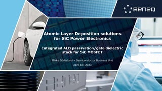
  • 1. Atomic Layer Deposition solutions for SiC Power Electronics Integrated ALD passivation/gate dielectric stack for SiC MOSFET Mikko Söderlund – Semiconductor Business Unit April 19, 2023
  • 2. 17.4.2023 – CONFIDENTIAL Company Introduction and More-than-Moore market focus Semiconductor ALD solutions and materials for SiC power devices Inflection in passivation/gate dielectric Introduction to ALD equipment Differentiated Beneq Transform® ALD cluster tool Outline
  • 3. 17.4.2023 – CONFIDENTIAL Semiconductor ALD products Beneq Transform® and C2 for the up to 200 mm MtM market Beneq Transform® 300 & C3 for the 300 mm MtM market Beneq Prodigy™ for Compound Semi and MEMS markets 200 mm and smaller wafers 300 mm wafers Prodigy™ Transform® Transform® Lite Transform® 300
  • 4. 17.4.2023 Semiconductor Markets we serve Power devices Image sensors R&D µOLED Advanced packaging RF Ics, Filters More-than-Moore device fabrication: ✓ Power devices ✓ RF Filter devices ✓ RF ICs ✓ CMOS image sensors ✓ µOLED ✓ LED, µLED, EEL, VCSEL, detectors and Si photonics ✓ MEMS, sensors and actuators ✓ Advanced Packaging (TSV, CSP) ✓ Smart Power ✓ Microcontroller and e-NVM ✓ RF, Analog and mixed signal 17.4.2023 – CONFIDENTIAL 300 mm * This presentation
  • 5. 17.4.2023 – CONFIDENTIAL BENEQ ALD Solutions for Power Devices Market segments Gate Dielectric (SiO2, High-k) Surface passivation Nucleation & seed, doping Metal & TCO Final Passivation (moisture barrier) Trench MOSFET ✓ ✓ ✓ SJ MOSFET ✓ ✓ ✓ IGBT ✓ ✓ ✓ SiC MOSFET & Trench MOSFET ✓ ✓ ✓ ✓ GaN HEMT ✓ ✓ ✓ ✓ ✓ Vertical GaN ✓ ✓ ✓ ✓ Plasma enhanced single wafer and/or sequential PEALD + thermal batch processing
  • 7. 17.4.2023 – CONFIDENTIAL SiC market drivers - devices and modules • 800 V battery systems enable fast charging and accelerate penetration of SiC devices and modules in BEV courtesy to their advantage over Si IGBT i.e. higher performance gain per unit cost for 1200 V SiC. • 1200 V SiC devices, in hybrid and full SiC modules, are supporting the raise of renewable energy capacity. 2021 device market 2021-2027 CAGR 685 M$ 39 % 37 M$ 24 % 145 M$ 19 % 78 M$ 16 % Power SiC 2022 | www.yole.fr| ©2022
  • 8. 17.4.2023 – CONFIDENTIAL SiC Power devices market forecast and market share • The SiC device market is expected to reach $6.1B by 2027. SiC has strongly penetrated the automotive market, which will represent more than 75% of the total SiC device market in 2027. • Despite the pandemic and semiconductor shortage in the past 2 years, SiC ramp ups are ongoing. EV/HEV is taking off, along with the transition from 400V to 800V battery systems. • The global SiC device market grew 57% in 2020-2021. Some major device suppliers performed at such rate. Power SiC 2022 | www.yole.fr| ©2022
  • 9. 17.4.2023 – CONFIDENTIAL Power SiC 2022 | www.yole.fr| ©2022 SiC MOSFET product development • Since market launch of SiC MOSFET early 2021, device manufacturers have released multiple generations of devices to support qualification in various applications. • Driven by lower ON resistance and smaller devices, Trench SiC MOSFET R&D started about 10 years ago.
  • 10. 17/04/2023 ALD inflection for SiC MOSFET Beneq Confidential
  • 11. 17.4.2023 – CONFIDENTIAL BENEQ ALD roadmap for SiC MOSFET T. Kimoto, Performance Improvement and Reliability Physics in SiC MOSFETs, IRPS 2022, Kyoto University Nitridation anneal post thermal oxidation Power SiC 2022 | www.yole.fr| ©2022 Reduced Ron Conformality & film quality BENEQ ALD roadmap Thermal ALD SiO2 w. anneal Plasma / thermal ALD SiO2 w. anneal Interface preclean and nitridation w. reduced anneal Introduce High k to replace SiO2 for higher reliability
  • 12. Materials & process solutions for SiC MOSFET 17.4.2023 – CONFIDENTIAL ✓ Optional** PEALD Nitride interfacial layer (AlN or Si3N4) • Further passivation of the SiC surface by nitridation • Effectively blocks oxygen to the SiC surface, leading to reduced Dit ✓ Deposition of gate dielectric (SiO2, High-k or SiO2/High-k) • Provide necessary performance as gate dielectric • High-k to improve reliability of the gate dielectric • Al2O3 or SiO2 acts as a capping material to prevent oxidation of the surface ✓ In-situ* plasma preclean to remove surface damage and/or provide surface nitridation of the surface • Remove cristal disorder at the surface SiC, Carbon clusters, caused by oxidation of SiC • Nitridation for passivation of SiC surface • Provide high quality interface for low density of interface states T. Kimoto et al. IEDM 2021 * In-situ to the PEALD process module ** alternative to NO Anneal
  • 13. Transform® Batch ALD performance – SiO2 Performance Value Breakdown (MV/cm) > 9.5 Leakage current density, @ 5 MV/cm (A/cm2) ~ 1 x 10⁻⁸ Refractive index @ 633 nm 1.45 Density (g/cm3) 2 Current vs. Electric Field Process temperature 300°C Wafer size 200mm WiW: ~ 0.6%, 1σ Wt: ~ 0.2%, 1σ BtB: ~ 0.26%, 1σ Throughput: 12 WPH @50 nm Pre-clean/treat and PEALD SiN is available on the single wafer plasma module 17.4.2023 – CONFIDENTIAL 25-wafer batch ToF-ERDA profile of thermal SiO2 As deposited thermal SiO2 O: 61.0 ± 0.6 at-% Si: 29.6 ± 0.5 at-% H: 9.4 ± 0.6 at-% C: <0.2 at-% (As deposited PEALD SiO2) O: 62.8 ± 0.6 at-% Si: 31.3 ± 0.5 at-% H: 5.8 ± 0.5 at-% C: <0.2 at-%
  • 14. SiO2 ALD / anneal integration - current status 17.4.2023 – CONFIDENTIAL Before annealing After annealing • Low hysteresis and fixed charges are obtained after anneal for both thermal and plasma ALD SiO2 • Plasma ALD SiO2 better control of the interface/trapped charges and will benefit of in-situ plasma pre-clean technology
  • 15. 17/04/2023 Beneq ALD equipment for the Wafer Fabs Beneq Confidential
  • 16. 17/04/2023 • Highly versatile cluster platform supporting a wide range of material and applications • Breakthrough in throughput with pre-heating and flow optimized mini-batch reactor design • Differentiated & patented sequential ALD processing combining plasma enhanced and thermal batch ALD for “best of both” worlds capability • Beneq Transform has become 1st choice for Tier1 IDM’s, Foundries and RTOs in Power, RF, MicroLED/Photonics, CIS, MEMS and Advanced Packaging Introducing Beneq Transform ® Beneq Confidential Versatile platform dedicated to More-than-Moore device fabrication Beneq Transform is your engine for the SiC materials revolution!
  • 17. 17/04/2023 Beneq Transform© enables sequential processing For best-of-both-worlds plasma enhanced and thermal ALD processing capability 2 Pre-heating module ✓ Productivity booster, > 40 % higher WPH ✓ Remove/outgas trace water and organics 2 3 Plasma-enhanced ALD process module ✓ Flexible single-wafer plasma chamber, direct or remote CCP type ✓ In-situ plasma pre-treatment/surface activation for reduced Dit ✓ For deposition of thin (e.g. 3-5 nm SiO2, AlN, SiN) interfacial layer (IL) 3 4 Thermal batch process module ✓ Receives wafers after SW PEALD process without air-break (in-vacuum transfer) ✓ Up to 25 wafer batch size ✓ For deposition of thicker dielectric layers e.g. 50-100 nm SiO2, or high-k Al2O3, HfO2…. 4 1 Load-lock ✓ Two load-locks, each for 25 wafer lot size 1 1 5 Cooling module ✓ For rapid cooling of wafers to < 60 C 5 3rd retrofit process module ✓ For example, 2nd PEALD chamber for additional capacity ✓ Or additional process capability such as Schottky contact, Final passivation, … High (double-digit ) WPH reached for pre-clean/IL/dielectric stack Beneq Confidential
  • 18. to customers’ developing needs. Add value as a caring community. Make it together continuously and step by step. Keep improving encouraging others to learn, too. Stay curious To fulfill our mission, we: www.beneq.com | info@beneq.com | +358 9 7599 530 mikko.soderlund@beneq.com Beneq is the home of atomic layer deposition. In 1984, we established the world’s first industrial production using ALD. Today, we lead the market with products for R&D (TFS 200, TFS 500, R2), semiconductor device fabrication (Transform®, Transform® 300, and ProdigyTM), 3D and batch production (P400A, P800, P1500), ultra-fast spatial ALD (C2R), and roll-to-roll ALD (Genesis).