National instruments track e
•Transferir como PPT, PDF•
4 gostaram•2,006 visualizações

The document discusses testing semiconductor chips using software-defined modular instrumentation. It describes challenges in testing mixed-signal ICs and outlines structural vs functional testing approaches. It then discusses specific test applications and instrumentation for MEMS devices, digital communication protocols, power management ICs, RF ICs, and more. National Instruments' PXI and LabVIEW platform is highlighted as enabling flexible, software-defined chip test solutions.

Recomendados
Mais conteúdo relacionado
Mais procurados
Mais procurados (20)
Destaque
Semelhante a National instruments track e
Semelhante a National instruments track e (20)
Mais de Alona Gradman
Mais de Alona Gradman (19)
Último
Último (20)
National instruments track e
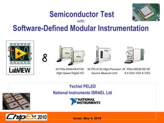
- 1. Semiconductor Test with Software-Defined Modular Instrumentation Yechiel PELED National Instruments ISRAEL Ltd & NI PXIe-6544/45/47/48 High-Speed Digital I/O NI PXI-4132 High-Precision Source Measure Unit NI PXIe-5663E/5673E 6.6 GHz VSA & VSG
- 2. Challenges in Testing Mixed-Signal ICs
- 9. Custom, Software-Defined Chip Test Graphical Programming Configuration Textual Math Modeling & Simulation Statecharts
- 12. PXI – PC-Based Modular Instrumentation Backplane - PCI bus communication - Timing and Synchronization Peripheral Instrument Modules - Over 1,500 modules from 70+ vendors Chassis - 4, 8 and 18 slot options Controller - Embedded PC, remote PC, or laptop interface - Runs all standard SW Systems Alliance
- 17. ImagingLab Robotics Library for DENSO - LabVIEW Toolkit for Directly Controlling DENSO Robotics Robotics- Wafers & components handling Robot places part at several known positions Vision reads part location at each position Software determines linear transfer function for X, Y and theta Coordinate Vision and Robot Space
- 18. Analog Instrumentation Digitizers and Arbitrary Waveform Generators
- 21. PXI and PCI Digitizers Model Description Platforms Input Channels Sampling Rate (S/s) Bandwidth (MHz) Resolution (bits) NI 5152/3/4 High-speed, high-bandwidth PXI, PCI 2 1 G (or 2 G on 1 ch) 300/500/ 1000 8 NI 5114 High-speed, low-cost PXI, PCI 2 250 M 125 8 NI 5124 High-resolution PXI, PCI 2 200 M 150 12 NI 5122 High-resolution PXI, PXIe, PCI 2 100 M 100 14 NI 5142 High-resolution, IF acquisition PXI, PCI 2 100 M 100 14 NI 5132/33 Low-cost, portable USB 2 50 M/100 M 50 8 NI 5105 High-density, low-cost PXI 8 60 M 60 12 NI 5622 High-resolution, IF acquisition PXIe 1 150 M 3 to 60 16 NI 5922 High-resolution PXI, PCI 2 15 M 6 24 to 16
- 22. NI & Tektronix collaborate on Fastest PXI Digitizer
- 23. High-Speed Signal Generators Function Generators Arbitrary Waveform Generators 5402 5404 5406 5412 5421 5422 5441 5442 Type Function Clock Function Arb Arb Arb Arb Arb Bandwidth 20 MHz 105 MHz 40 MHz 20 MHz 43 MHz 80 MHz 43 MHz 43 MHz Sample Rate 400 MS/s 300 MS/s 400 MS/s 100 MS/s 100 MS/s 200 MS/s 100 MS/s 100 MS/s Resolution (bits) 14 12 16 14 16 16 16 16
- 25. Digital Instrumentation Digital Waveform Generators / Analyzers, FPGA-Enabled I/O
- 29. NI PXI High Speed Digital Offering PCI / PXI-6541/42 PXIe-6544/45 PXIe-6547/48 PCI / PXI-6551/52 Max Speed 50 / 100 MHz 100MHz / 200 MHz 100MHz / 200 MHz 50 / 100 MHz Platform PCI / PXI PXI Express PXI Express PCI / PXI # of Channels 32 32 32 / 24 (with HWC) 20 Direction Input or Output Input or Output In/Out or Bidirectional Bidirectional Precision CLK No Yes Yes No Max DDR No No 400/300 Mbps (out/in) No Voltage Levels Selectable 1.8, 2.5, 3.3, 5V* Selectable - 1.2, 1.5, 2.5, 1.8, 3.3 V Selectable 1.2 - 3.3V (100 mV res.) Programmable -2 to 5V (10 mV res.) HWC / Tri-state No No Yes (24 ch) Yes (20 ch) Streaming 115 MB/s 400 / 660 MB/s 400 / 660 MB/s 115 MB/s
- 33. Precision DC Instrumentation Multimeters, Power Suppliers, Source Measure Units
- 35. NI PXI Power Supply / SMU Offering NI PXI-4110 Power Supply NI PXI-4130 Power SMU NI PXI-4132 Precision SMU Target Apps 3-channels - Power source/readback High power (40W) IV sweeps, Low-power (2W) leakage testing Max Voltage +6V, +20V, -20V +/-20V +/- 100V Max Current 1A on each channel +/- 2A +/- 100mA (2W max) 4-quadrant No Yes Yes Current Meas. Sensitivity 400 nA 1 nA 10pA Integrated Guarding No No Yes Output timing Software Timed Software Timed SW or HW timed Triggering No No Yes – PXI backplane
- 39. RF Instrumentation Vector Signal Generators / Analyzers and Modulation Software
- 42. MIMO - Four Channel of Phase-Coherent VSA Local Oscillator Downconverters Digitizers Shared LO Shared ADC Clock
- 45. NI RIO Technology Platform RIO = FPGA based Reconfigurable I/O
- 49. What is Non-Destructive Test? The use of noninvasive techniques to determine the integrity of a material, component or structure or quantitatively measure some characteristic of an object. i.e. Inspect or measure without doing harm.
- 50. Video Testing ( Analog to HDMI)
Notas do Editor
- National Instruments Leadership Seminar April, 2002 National Instruments CONFIDENTIAL
- Changes in both space - transition Created an opportunity for COTS hardware in this market Two elements (char / production) ACTION - Change bullets to better list challenges vs what each phase Talking points - setup challenges in both areas MAKE ACTION Oriented
- Team full of people designing circuit functionality, then laying it out with crazy cad tools. Also considering that it needs to be tested and built easily. Once those guys finalize a design and all their simulations are looking good, they kick it off for a first production run (similar to an MVR at NI). It gets built into wafers and finally packaged chips, and the engineers are just waiting to get their hands on these chips to test them. More than likely, there are 1 or 2 out of 100 that actually work, so they analyze the reasons why, tweak the design and figure that stuff out during their process of validation. Once they are satisfied and the tweaks are all set, the chip gets kicked off for production of 1000s or millions. So again, the important thing is that it’s the story of 3 labs… So – where do you think NI should attack? (production) - anyone think validation? Well lets start at the top of the list… Circuit design – while we do have multisim, its pretty cut and dry that it isn’t going to do the job – this isn’t an intro to circuits class, this is the most rigirous big-science designs going on, and they have VERY specialized CAD tools. Circuit design is pretty much out. Lets take a look at proudction. Story of 3 different Labs… A typical IC design cycle involves several steps: Feasibility study and die size estimate Functional verification Circuit design Circuit simulation Floorplanning Design review Layout Layout verification Layout review Design For Test and Automatic test pattern generation Design for manufacturability (IC) Mask data preparation Wafer fabrication Die test Packaging Device characterization Tweak (if necessary) Datasheet generation
- 2 main types of test that can be done on either the production floor or in the validation lab
- Notes: This is still structural test. Boils down to a limit test for certain features – outside of certain range, device is failing. Two main flavors. DC and AC.
- What is NI LabVIEW? LabVIEW is a highly productive graphical development environment with the performance and flexibility of a programming language, as well as high-level functionality and configuration utilities designed specifically for measurement and automation applications. In general-purpose programming languages, the code is as much of a concern as the application. You must pay close attention to the syntax (commas, periods, semicolons, square brackets, curly brackets, round brackets, etc.). In contrast, with LabVIEW you use icons to represent functions, and you wire them together to determine the flow of data through your program, similar to creating flowcharts. It has all the breadth and depth of a general-purpose programming language, but it is easy to use, increasing your productivity by decreasing the time required to develop your applications. You can easily divide measurement and automation application into three main parts: acquisition, analysis, and presentation of data. LabVIEW provides a seamless way to acquire your data, perform necessary analysis on that data, and present the information in a chosen format. Throughout the seminar, we touch upon each of these three components of a measurement and automation application. Each program in LabVIEW is called a virtual instrument, or VI. The VI serves as the primary building block of a LabVIEW application, and you can use it to modularize your code for efficient design, clear and concise documentation, and simplified maintenance. Each LabVIEW VI is made up of three main components: the Front Panel, Block Diagram, and the Palettes. In the coming slides, we continue our discussion of the actual development environment of LabVIEW. © National Instruments Corporation LabVIEW Graphical Development Hands-On Seminar
- Over the last 21 years, LabVIEW has evolved from a programming environment primarily used to develop instrument control and data acquisition tasks to a graphical system design platform used for test, control and design applications that can be deployed to a variety heterogeneous processing platforms such as FPGA and real-time processor systems. The ability to mix development methods in these applications enables you to use the best technique to solve each aspect of your challenge. Configurable, code-generation utilities such as LabVIEW Signal Express and a variety of assistants provide a short learning curve even when developing complex applications. The MathScript node and formula node allow you to mix textual math algorithms to your LabVIEW applications while the statechart module and simulation module provide a higher level of abstraction for solving certain problems. All of these development techniques are tied together by LabVIEW graphical programming to provide a complete graphical system design platform for you test, control and design applications.
- National Instruments offers a wide selection of these PXI modular instruments including the industry’s highest-resolution digitizer with 24 bits of resolution and up to 1 GHz of real-time bandwidth, power supplies and source measure units with nanoamp precision, the industry’s fastest, most accurate 7 ½ digit digital multimeter, high-speed digital waveform generation and acquisition with data rates as high as 400 MB/s, highest-channel-count dynamic signal acquisition, and RF instruments with up to 6.6 GHz generation and 26.5 GHz acquisition.
- PXI systems are comprised of three basic components – chassis (which includes the PXI backplane), controller, and peripheral modules. The chassis provides the rugged and modular packaging for the system. Chassis range in size from 4 to 26 slots. The chassis contains the high-performance PXI backplane, which includes the PCI bus and timing and synchronization buses. All PXI systems include a controller. Controller options include remote control from standard desktop and laptop PCs, 1U rackmount controllers, and high-performance embedded controllers. Because PXI embedded controllers are built using standard PC components, they run standard operating systems, such as Windows XP, and applications, such as Microsoft Excel. Over 1,000 different peripheral modules are available from the 70+ members of the PXISA. Modules are available for instrumentation, data acquisition, control, interfacing to buses, etc.
- The PXI module of choice for providing the analog stimulus to ADCs is a high-speed function generator. For instance, the PXI-5406 can generate sine waves up to 40MHz with 16 bit resolution. National Instruments PXI signal generators also include versatile arbitrary waveform generators, such as the NI 5421, as well as RF vector signal generators. Whether generating simple sine and clock signals or complex I/Q modulated communications waveforms, the broad NI offering of signal generators can improve your prototyping and test systems by offering world-class generation performance and higher system throughput.
- LabVIEW FPGA 1.1 Module - AE Continuous Training May 2004 National Instruments CONFIDENTIAL Another key application for FPGA hardware is implementing digital protocols. Digital protocols are used in a wide variety of applications to communicate between different components on a plug-in board or within a computer, or to connect different subsystems within a car or an airplane. They are used to transfer audio from your DVD player to your stereo or to pass the information from the touchpad on your laptop to the motherboard and processor. Being able to read, write and monitor such protocols is a critical part of many test applications to verify and control the operation of different components as well as their interfaces. Some of these interfaces have commercial off-the-shelf hardware that may be purchased, but many times these communication interface devices require custom hardware to be built. With LabVIEW FPGA, you can simply configure the FPGA to control the digital lines to implement many communication protocols requiring tight timing and synchronization.
- One classic example of functional testing that we’ve been doing well with is BERT
- The PXIe-6544/45 and PXIe-6547/48 expand NI’s high-speed digital offering overall. They are also our first high-performance PXI Express digital instruments, and feature the industry’s fastest streaming rates at up to 660 MB/s.
- The new NI PXIe-6545 digital waveform generator/analyzer features 32 bidirectional channels clocked at a maximum of 200 MHz. The selectable voltage levels of 1.2, 1.5, 1.8, 2.5, and 3.3 V work with the most common logic levels and are ideal for conducting tests on semiconductor devices, such as analog-to-digital converters (ADCs), digital-to-analog converters (DACs), ASICs, and microcontrollers. They also feature an onboard DDS clock to provide subhertz resolution up to 200 MHz, helping you clock data (generation or acquisition) with higher precision without using an external clock. The PXIe-6547/48 add on to the features of the PXI-6544/45 to offer 3 banks of data delay to skew edges on different DIO lines by separate values, real-time comparison of acquired data vs expected response data (HW compare), DDR capabilities up to 400 Mbps, and more flexible voltage levels, up to 22 across the entire range of 1.2 to 3.3V with 100 mV precision.
- Import. Read VCD, EVCD, WGL, or STIL. Waveform Analyze. Automatically detect clock cycles or apply user-specified cycle to gather all waveforms found in the source VCD/EVCD. Note that this is waveform-based, which provides the most accuracy cyclization (as opposed to sample technique commonly used where design intents are compromised). If source files are WGL or STIL, this step can be skipped. Cyclizer. Simply binding pattern bits to the waveforms/timing extracted in the previous step. Again, if source files are WGL or STIL, this step can be skipped. TesterBridge. This last step applies tester rules checks, tester specific resource allocation, and tester files generation.
- LabVIEW FPGA 1.1 Module - AE Continuous Training May 2004 National Instruments CONFIDENTIAL Explain why FPGA makes sense for communications protocols. Also introduce protocol aware and describe. You want your own slide for that?
- Finally, here is a comparison of NI’s precision DC sources.
- The NI PXI-4132 is a programmable, high-precision source measure unit (SMU) in a single-slot, 3U PXI module. It has a single, isolated SMU channel that offers a four-quadrant, ±100 V output incorporating remote (4-wire) sense as well as external guarding. This channel is capable of sourcing and sinking up to 2 W maximum. It can source and sink currents up to 20 mA at up to 100 V, currents up to 50 mA at up to 40 V, and currents up to 100 mA at up to 20 V. With measurement resolution down to 10 pA and integrated guarding, the PXI-4132 precision source is ideal for high-accuracy leakage measurements on integrated circuits, discrete components, PCBs, and cables. You can also perform high-speed I-V measurements on a variety of components including diodes and organic LEDs using the onboard hardware sequencing engine. In addition, you can synchronize multiple PXI-4132 SMUs via the PXI backplane to provide high-speed I-V measurements on transistors and more complex devices.
- If it IS drawing too much power, that’s a big clue that there’s some horrible short on the inside and if this chip was used in its final environment, it would totally blow something up…
- NI has a comprehensive platform of instrumentation hardware and software for RF and communications design and test. For RF and microwave hardware, there is the vector signal analyzers and generators, continuous-wave (CW)-based signal generators, preamplifiers and RF and microwave switches. However, NI has a world-class IF and baseband offering of digitizers and arbitrary waveform generators for intermediate frequency analysis and generation in PXI including high-speed digital for advanced digital RF applications. NI’s IF platform is very tightly integrated with our LabVIEW software and offers a great platform for integrating into hybrid systems with standalone, GPIB, LAN, 3 rd -party PXI and VXI up- and downconverters for completely user-defined systems. NI’s RF and communications software is centered around LabVIEW for graphical programming and LabWindows/CVI for text-based programming. The specific toolkits designed to aid in RF and communications are the Modulation Toolkit and the Spectral Measurements Toolkit. The Modulation Toolkit is an add-on for communication and protocol generation and analysis while the Spectral Measurements Toolkit is designed for RF spectral analysis applications.
- NI’s RIO technology platform offers a unique and standard architecture that consists of a processor + FPGA + I/O for design , control and test applications. Because the FGPA is tightly integrated into the architecture, it offers unprecedented co-processing, timing and control benefits. Now on the hardware side, the RIO architecture is delivered in a variety of form factors that go from packaged to board level options. These reconfigurable, off the shelf platforms are open and easily integrate with 3 rd party hardware and offer a breadth of I/O alternatives that range from analog, vision, motion, RF, etc.
- I have asked out mechanical engineers for new drawings that should make this look much better. Another option would be photographs.
- The NI 5752 is a 32 channel digitizer adapter module capable of sampling on all channels simultaneously at 50 MS/s with 12-bit resolution. The board is optimized for non-destructive test applications with 100 ohm differential inputs, AC coupling, and built-in ADC features like selectable anti-alias filters and programmable gain control. It also has 16 digital outputs, which NDT customers may want to use to interface to external power amplifiers to create an array of high voltage pulser channels, a common need in NDT applications. The board is designed with the intention that the customer will add their own signal conditioning and input protection, interfacing primarily with ultrasonic transducers. So, we're providing a core, off-the-shelf building block that will be really useful for customers who would normally design their own solution from scratch, and we have also seen interest from OEMs who want to build complete systems around it. Some applications like phased array systems can have very high channel counts, commonly 128 or 256 channels.
- The PXI-5114 cards are sampling Y, Pb, and Pr at 250MS/s with 8bit resolution The luma signal (Y) carries the video trigger which represents the beginning of a new line -Ch0 of card A looks for signal, then begins sampling on all three channels -At least 15,000 samples are recorded and sent to controller 3. The samples represent the scan along a signal horizontal line -Indexing along these lines allows us to pick out specific colors from test pattern -RGB values for each color can be compared to threshold values