Mais conteúdo relacionado
ASU Zhang Nature Energy paper on CdTe DH_5_16_2016
- 1. ARTICLES
PUBLISHED: 16 MAY 2016 | ARTICLE NUMBER: 16067 | DOI: 10.1038/NENERGY.2016.67
Monocrystalline CdTe solar cells with open-circuit
voltage over 1 V and efficiency of 17%
Yuan Zhao1,2
, Mathieu Boccard2
, Shi Liu1,2
, Jacob Becker1,2
, Xin-Hao Zhao1,3
, Calli M. Campbell1,3
,
Ernesto Suarez1,2
, Maxwell B. Lassise1,2
, Zachary Holman2
and Yong-Hang Zhang1,2
*
The open-circuit voltages of mature single-junction photovoltaic devices are lower than the bandgap energy of the absorber,
typically by a gap of 400 mV. For CdTe, which has a bandgap of 1.5 eV, the gap is larger; for polycrystalline samples, the
open-circuit voltage of solar cells with the record efficiency is below 900 mV, whereas for monocrystalline samples it has only
recently achieved values barely above 1 V. Here, we report a monocrystalline CdTe/MgCdTe double-heterostructure solar cell
with open-circuit voltages of up to 1.096 V. The latticed-matched MgCdTe barrier layers provide excellent passivation to the
CdTe absorber, resulting in a carrier lifetime of 3.6 µs. The solar cells are made of 1- to 1.5-µm-thick n-type CdTe absorbers, and
passivated hole-selective p-type a-SiCy:H contacts. This design allows CdTe solar cells to be made thinner and more efficient.
The best power conversion efficiency achieved in a device with this structure is 17.0%.
S
ilicon and GaAs solar cells have recently been demonstrated
with efficiencies that are 87% of their respective detailed-
balance limits1
. Like Si and GaAs, CdTe has a near optimum
bandgap and a high absorption coefficient near the band edge, and
is thus an excellent material for photovoltaic technology2
. However,
the efficiency of the best CdTe cell is only 67% that of its detailed-
balance limit owing to excessive non-radiative recombination1
and
the difficulty in forming hole contacts by p-type doping3
. Indeed,
the record Si and GaAs cells have monocrystalline absorbers with
wide-bandgap barrier/passivating layers at the absorber interfaces4
,
whereas the record CdTe cell has a polycrystalline absorber.
Furthermore, existing CdTe cell structures do not have a wide-
bandgap material that can both provide carrier confinement and
also offer a low interface recombination velocity (IRV)1
. The cells
thus have a low open-circuit voltage (Voc) of 0.876 V compared to
a detailed-balance Voc of 1.23 V; this is largely responsible for the
relatively low efficiency of CdTe cells5
.
High quasi-Fermi-level splitting is a prerequisite for high Voc, and
requires long bulk carrier lifetime and low IRV. However, typical
lifetimes in polycrystalline CdTe thin films are of the order of only
several nanoseconds6
, which, together with low achievable doping
levels in the p-type regions, limit the quasi-Fermi-level splitting, and
thus the Voc to 0.936 V. Assuming an acceptor density of 1015
cm−3
and a carrier lifetime of 66 ns, as was demonstrated in bulk CdTe6
, a
Voc as high as 1.026 V should have been possible as early as 1987, yet a
Voc of only 0.910 V was measured for a monocrystalline CdTe wafer,
a record that stood for decades7
. This impasse seems recently to have
come to an end as interest in the material system has resurfaced
and voltages over 1 V have been demonstrated in a monocrystalline
CdTe cell8
. For the standard polycrystalline CdTe cell configuration
with a CdS layer at the front and a metallic layer at the back, an IRV
of approximately 105
cm s−1
was measured6
, thereby limiting the
effective lifetime to a few nanoseconds and the maximum possible
Voc to roughly 0.9 V, depending on the CdTe thickness6
.
Provided that excellent bulk carrier lifetime and low IRV are
achieved, the high chemical potential (quasi-Fermi-level splitting)
must be extracted at the contacts as an electrical potential to
achieve high Voc. For conventional polycrystalline thin-film CdTe
solar cells, the n-type CdS layer at the front has a typical donor
density of approximately 1018
cm−3
and acts as an effective electron
contact9
, while a lightly p-type doped CdTe absorber layer is used in
conjunction with an additional hole contact. This results in a built-in
voltage (Vbi) inside the cell that is smaller than the achievable quasi-
Fermi-level splitting in the absorber material5,10
, so that the chemical
potential cannot be fully extracted as an electrical potential.
This paper addresses the three challenges to achieving high Voc
and high efficiency in CdTe solar cells: long bulk carrier lifetimes,
low IRV, and a heavily doped p-type contact. Using epitaxial CdTe
as a demonstration platform, and employing new passivation and
p-type contact layers in a double-heterostructure cell design, we
demonstrate a Voc beyond the 1 V barrier and a substantial increase
in efficiency for monocrystalline CdTe solar cells.
Absorber quality and interface optimization
To achieve long carrier lifetimes, we leverage high-quality CdTe
epitaxially grown on InSb (001) substrates using molecular beam
epitaxy (MBE)11
and CdTe/Mgx Cd1−x Te double-heterostructure
(DH) designs11–13
. The complete desorption of the oxide layer on
InSb substrates under a Sb flux and the near-perfect lattice match
between InSb and both CdTe (0.03% mismatch) and MgTe (0.9%
mismatch) enable extremely low defect density, and thus very good
structural and optical properties. The DH designs offer optimal
confinement for minority carriers and excellent passivation of the
surfaces of the CdTe absorber layer.
To reduce the IRV, we employ a DH in which a CdTe
absorber layer is sandwiched between two Mgx Cd1−x Te barrier
layers. These wide-bandgap barriers effectively confine the minority
carriers to the narrower-bandgap CdTe absorber14,15
. Furthermore,
the CdTe/Mgx Cd1−x Te interfaces themselves are close to perfect,
eliminating recombination-active defects at the absorber interfaces.
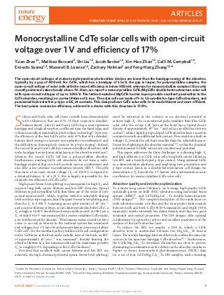
Figure 1a shows time-resolved photoluminescence (TRPL) data
for a set of four CdTe/Mgx Cd1−x Te DH samples, each consisting
1
Center for Photonics Innovation, Arizona State University, Tempe, Arizona 85287, USA. 2
School of Electrical, Computer and Energy Engineering, Arizona
State University, Tempe, Arizona 85287, USA. 3
School for Engineering of Matter, Transport and Energy, Arizona State University, Tempe, Arizona 85287,
USA. *e-mail: yhzhang@asu.edu
NATURE ENERGY | www.nature.com/natureenergy 1
© 2016 Macmillan Publishers Limited. All rights reserved
- 2. ARTICLES NATURE ENERGY DOI: 10.1038/NENERGY.2016.67
0 250 500 750 1,000 1,250 1,500 1,750
Seff = 1.2 ± 0.7 cm s−1
Seff = 1.4 ± 0.6 cm s−1
PLintensity(a.u.)
Time (ns)
2.8
dCdTe (nm)
348
541
220
3.6
272
2.2
2.2
3 4 5 6 7 8 9 10
2/d (μm−1)
0.2
0.3
0.4
0.5
0.6
0.7
0.8
0.9
1.0
1.1
1.2
0.00
0.05
0.10
0.15
0.20
0.25
0.30
0.35
1/non(μs−1)τ
eff (μs)τ
a b
Figure 1 | CdTe double-heterostructure photoluminescence decay and interface recombination velocity. a, Normalized room-temperature time-resolved
photoluminescence decay for a set of four DH samples, each consisting of two 30 nm Mg0.46Cd0.54Te barriers and a CdTe layer with a thickness between
220 nm and 541 nm. The curves have been shifted along the y-axis for clarity. The fitted lifetimes are shown in the inset table. b, Inverse non-radiative
recombination lifetime 1/τnr versus inverse CdTe layer thickness 2/d. The effective interface recombination velocities were extracted by fitting these data.
The error bars of 1/τnon were determined by considering the uncertainty of the estimated radiative lifetimes due to the estimation of doping densities.
of two 30-nm-thick intrinsic Mg0.46Cd0.54Te barriers and a CdTe
middle layer with n-type background doping of the order of
1014
cm−3
and a thickness between 220 nm and 541 nm, which was
determined by detailed analysis of high-resolution X-ray diffraction
measurements. All samples exhibit effective carrier lifetimes—
determined by fitting single exponentials to the TRPL decay tails—
exceeding 2 µs, which attests to the high quality of the CdTe layers
and the CdTe/Mgx Cd1−x Te heterointerfaces. The longest lifetime of
3.6 µs is substantially longer than the previous records for crystalline
bulk CdTe (ref. 6) and CdTe/Mgx Cd1−x Te DHs (refs 12,13).
The IRV can be parsed by varying the CdTe bulk layer thickness.
The expression for effective (measured) lifetime τeff is shown in
equation (1), where τrad and τnon are the radiative and non-radiative
lifetimes, respectively. The radiative lifetime is related to the photon
recycling factor γ (ref. 16), the material radiative recombination
coefficient B, and the doping concentration ND. Because the photon
recycling effect is stronger for thicker samples, the radiative lifetime
becomes longer for DH samples with thicker CdTe absorber layers.
The non-radiative lifetime is related to the bulk Shockley–Read–
Hall (SRH) lifetime τSRH and the interface recombination. In
equation (1), Seff is the effective IRV and d is the thickness of the
CdTe layer.
1
τeff
=
1
τrad
+
1
τnon
=(1−γ)BND +
1
τSRH
+
2Seff
d
(1)
Because the radiative lifetime is dependent on the sample thickness,
only the non-radiative lifetimes were used to extrapolate the
effective IRV; the non-radiative lifetimes were calculated from the
measured effective lifetimes and an estimated radiative lifetime. The
radiative lifetime was calculated assuming B = 4.3 × 10⁻⁹
cm3
s−1
,
ND = 1.5 × 10¹⁴
cm−3
, and an error bar of ±25% for the estimation
of the doping concentration17
. Figure 1b plots the inverse non-
radiative lifetime (1/τnr) versus the inverse CdTe layer thickness
(2/d) for the four samples shown in Fig. 1a, which have 30-nm-
thick Mg0.46Cd0.54Te barriers, and another set of four samples with
identical layer structure and alloy composition but with 22-nm-
thick barriers. Weighted fittings of the data using the error bars
yield effective IRVs of 1.2 ± 0.7 cm s−1
and 1.4 ± 0.6 cm s−1
,
which are comparable to or better than the best values reported for
GaAs/Al0.5Ga0.5As (18 cm s−1
) and GaAs/Ga0.5In0.5P (1.5 cm s−1
)18,19
.
CdTe solar cell design
The studied device structure shown in Fig. 2a affords new
opportunities with respect to addressing the challenge of p-type
doping in CdTe: with interface passivation provided by the
Mgx Cd1−x Te barrier layers, the contact layers can be defective. Such
a desirable property enables a much broader choice of contact-
layer materials, which may be either crystalline or amorphous.
This structure maintains the voltage of the solar cell by preventing
the contact layers from compromising the absorber quality, as the
minority carriers in the CdTe absorber will be confined by the
barriers. That is, heterostructure barriers offer an alternative way to
construct a junction in CdTe solar cells that circumvents the major
challenge of p-type doping and opens the door to many novel device
structure designs—a similar approach is used in HIT solar cells20
.
One caveat is that the front contact layer should be as transparent
as possible to minimize parasitic absorption, which reduces the
photogenerated current of the solar cell.
We used a 5- to 15-nm-thick heavily doped p-type amorphous
silicon (a-Si:H, estimated doping level of 1018
cm−3
) or amorphous
silicon carbide (a-SiCy :H, y ∼ 6%) layer as the p-type contact.
These layers were deposited by plasma-enhanced chemical vapour
deposition on the front Mgx Cd1−x Te barrier, followed by an indium
tin oxide (ITO) electrode deposited by sputtering (Fig. 2a). The
schematic band diagrams are shown in equilibrium in Fig. 2b and
at open circuit in Fig. 2c. The intent of the design is that the
barrier/contact stacks block the transport of minority carriers to the
contacts while permitting majority carriers to flow unimpeded—
minority carriers referring to the minority carrier type of each
respective contact layer, not the absorber. The Mgx Cd1−x Te barrier
at the front (hole-contact side) should be properly chosen, without
compromising the effectiveness of its passivation of the CdTe
absorber, to enable transport of holes across the barrier while
simultaneously blocking electrons by the large conduction-band
offset. Note that the simulated open-circuit band diagram in Fig. 2c
indicates a small Voc loss at the p-type contact because of the negative
valence-band offset between a-Si:H and CdTe. The motivation for
2
© 2016 Macmillan Publishers Limited. All rights reserved
NATURE ENERGY | www.nature.com/natureenergy
- 3. NATURE ENERGY DOI: 10.1038/NENERGY.2016.67 ARTICLES
Electrode ITO
n-Mg0.24Cd0.76Te
(ND = 5 × 1017 cm−3)
n-CdTe
(ND = 5 × 1017 cm−3)
n-InSb
(ND = 5 × 1017 cm−3)
n-InSb
substrate
n-CdTe
n-CdTe
n-CdTe
n-CdTe
n-MgCdTe
n-MgCdTe
MgxCd1−xTe
a-SiCy:H
MgCdTe
a-SiCy:H
a-Si:H
i-MgCdTe
Contact layer
Absorber
Back side
barrier
Contact layer
Buffer
Conduction band
Voc
Quasi-Fermi levels
Valence band
0
−2.0
−1.5
−1.0
−0.5
0.0
Energy(eV)
0.5
1.0
1.5
2.0
100 200 300
Distance from surface (nm)
1,400 1,650
Front side
barrier
a b
c
d
Figure 2 | Device design and band diagram. a, Layer structure of the CdTe/MgxCd1−xTe DH solar cell with an a-SiCy:H (y = 0–6%) hole-contact layer.
b–d, Schematic band diagrams at equilibrium (b) and open circuit (c) and an equilibrium band diagram drawn to scale for the hero cell (d). The band
diagrams shown in b and c represent several different structure designs and are thus not drawn to scale with respect to energy and length. The parameters
used for the calculation are given in Table 1.
Table 1 | Parameters used for the quantified band diagram calculation.
ITO a-Si:H i-MgCdTe n-CdTe n-MgCdTe
Bandgap 4 eV 1.8 eV 2.088 eV 1.5 eV 1.97 eV
Electron affinity 4.9 eV 3.9 eV 3.871 eV 4.28 eV 3.951 eV
Doping n-type p-type Intrinsic n-type n-type
Doping density Degenerate 1 × 10¹⁸
cm−3
NA 1 × 10¹⁶
cm−3
5 × 10¹⁷
cm−3
Intrinsic carrier concentration Metal-like 8 × 10⁴
cm−3
6 × 10³
cm−3
5 × 10⁵
cm−3
6 × 10³
cm−3
Nc/Nv Metal-like 1 0.144 0.144 0.144
Thickness 70 nm 8 nm 10 nm 1.4 µm 50 nm
adding carbon to form a-SiCy :H is to achieve a smaller valence-band
offset, and thus a lower voltage drop. As the conduction-band offset
is large, the 50-nm-thick Mg0.24Cd0.76Te barrier at the back (electron-
contact side) was heavily doped n-type to facilitate transport of
electrons and impede holes.
Although more than eight wafers of different designs were used
for the study reported here, we focus on the following two designs in
this paper: Design A consists of a hole-contact layer (8 nm a-SiCy :H
+ 4 nm a-Si:H, y ∼ 6%), a 10-nm-thick undoped Mg0.30Cd0.70Te
front barrier, and a 1-µm-thick absorber with n-type In doping
of 3 × 10¹⁶
cm−3
; Design B consists of a hole-contact layer (8 nm
a-Si:H), a 10-nm-thick undoped Mg0.30Cd0.70Te front barrier, and a
1.4-µm-thick absorber with n-type In doping of 1 × 10¹⁶
cm−3
for
the top 1 µm and 5 × 10¹⁷
cm−3
for the bottom 0.4 µm. Figure 2d
shows an equilibrium band diagram drawn to scale for the hero cell
design (Design B) with the highest efficiency.
Solar cell characterization
After the growth of the underlying DH, the wafers were processed
into devices. Figure 3a shows the average and maximum Voc of a
series of solar cells with 8- to 12-nm-thick a-Si:H and a-SiCy :H
hole-contact layers. For each contact material, the front Mgx Cd1−x Te
barrier width and height (Mg composition, x) were also explored. A
(low) Voc was measured even in the absence of an intentional hole-
contact layer, because ITO itself is slightly hole selective with its
relatively high work function of 4.8 eV. Inserting a heavily doped
p-type a-Si:H contact layer yields a greatly enhanced Voc because
of the increase in Vbi, which we determined to be 1.1 V using
capacitance–voltage (C–V) measurements. As anticipated from
TRPL studies of DHs, the Voc rises as the front barrier height
or width increases because electrons are further confined to the
CdTe absorber layer as thermionic emission and tunnelling are
suppressed. The Voc further increases—to a maximum measured
value of 1.096 V—when p-type a-SiCy :H is used, which has a wider
bandgap and lower (negative) valence-band offset than that of a-
Si:H. The solar cells with the highest Voc values, however, do not
tend to have the highest efficiencies owing to smaller fill factors (FF).
Figure 3b shows the FF against the Voc for all solar cells measured so
far; notice that the cells with a-SiCy :H all have lower FF than their
a-Si:H counterparts. We attribute the large FF loss to a lower doping
level than that in the a-Si:H layer, which inhibits transport across the
heterojunction interfaces between the a-SiCy :H hole-contact layer
and the ITO layer and Mgx Cd1−x Te front barrier layer; this effect
effectively increases the lumped series resistance of the cell.
A 0.21-cm2
solar cell of Design A and an evaporated silver
front grid was tested by the National Renewable Energy Laboratory
(NREL). The certified current–voltage and external quantum
efficiency (EQE) characteristics are shown in Fig. 4a and indicate
an efficiency of 14.66% ± 1.4%. Although the Voc of this particular
device is slightly under 1 V at 0.9954 V ±0.3%, another device
of Design B had a certified Voc of 1.0542 V ±0.5%, which is
approximately 150 mV greater than the long-standing record, and
nearly 40 mV greater than the recently demonstrated 1 V devices7,8
.
Measurements of further devices with set-ups calibrated using
the device measured by NREL in the authors’ laboratories reveal that
many devices of Design A have demonstrated Voc consistently over
1 V without greatly sacrificing the output power under operating
conditions, and the best tested device (Design B) had a Voc of
1.036 V, a Jsc of 22.3 mA cm−2
, a FF of 73.6%, and a power
conversion efficiency of 17.0%, as shown in Fig. 5a. The maximum
Voc measured from all the tested devices was 1.096 V, which is quickly
approaching the theoretical limit of 1.17 V for CdTe solar cells with
NATURE ENERGY | www.nature.com/natureenergy
© 2016 Macmillan Publishers Limited. All rights reserved
3
- 4. ARTICLES NATURE ENERGY DOI: 10.1038/NENERGY.2016.67
0.4
ITO a-Si:H
Hole-contact layer Open-circuit voltage, Voc (V)
Barrier thickness (nm)
a-SiC:H 0.4 0.5 0.6 0.7 0.8 0.9 1.0 1.1 1.2
0.5
0.6
0.7
0.8
0.9
Open-circuitvoltage,Voc(V)
Fillfactor,FF(%)
1.0
1.1 30%
Mg
40%
1.2
0
10
20
30
40
50
60
70
80
90
a-Si:H
a-SiCy:H
ITO only
10
a b
5 10 5 10
Figure 3 | Effects of different passivation and contact layers on device performance. a, Box plot indicating the average and maximum Voc for several solar
cell designs with different hole-contact layers and barrier thicknesses and heights. The upper and lower bounds of the boxes indicate the 25th and 75th
quartiles. b, FF versus Voc for all individual devices measured and analysed for a.
0
0.0 0.2 0.4 0.6
Voltage (V)
300 400 500 600 700 800 900
Wavelength (nm)
0.8 1.0 1.2
5
10
15
Currentdensity(mAcm−2)
0
20
40
JPhoto = 23.93 mA cm−2
Device parameters:
Jsc = 21.663 mA cm−2 ± 1.4%
Voc = 0.9954 V ± 0.3%
FF = 67.98% ± 0.4%
= 14.66% ± 1.4%η
60
80
100
Externalquantumefficiency(%)
20
25a b
Figure 4 | NREL certified device results. J–V curve (a) and EQE (b) for a sample with a 10-nm-thick Mg0.30Cd0.70Te barrier and an 8-nm-thick a-Si:H
hole-contact layer. The device under test is square with an area of 0.21 cm2
.
an absorbing substrate. All these device characteristics are greater
than the previous records of Voc (1.017 V) and efficiency (15.2%) for
monocrystalline CdTe (ref. 8). The significant increase in both Voc
and conversion efficiency is attributed to the much improved bulk
carrier lifetime and reduced IRV through the use of Mgx Cd1−x Te
passivation/barrier layers, and the heavily doped a-Si:H or a-SiCy :H
hole-contact layer.
The Jsc values of both Design A and B are also higher than
the previous record monocrystalline cell7
, primarily owing to the
higher quantum efficiencies at shorter wavelengths (below 600 nm),
as seen in Fig. 5b. An AM1.5G-weighted integration of the EQE,
shown in blue, provides a Jsc of 22.3 mA cm−2
. However, there is
still considerable current loss, as indicated by the large gap between
the EQE and 1 − R curves. The loss in this region is attributed to
parasitic optical absorption in the ITO, highly defective a-SiCy :H,
and Mgx Cd1−x Te layers, as well as transmission loss. The breakdown
of these different losses by their mechanisms and the simulated
absorptance of this structure are shown in Fig. 5c. The ITO, a-Si:H
and Mgx Cd1−x Te layers all absorb incident sunlight before it reaches
the CdTe absorber, and are responsible for Jsc losses of 1.2 mA cm−2
,
1.4 mA cm−2
and 0.6 mA cm−2
, respectively. Using a thinner hole-
contact layer or a wider-bandgap material can drastically reduce the
parasitic optical absorption at these energies, resulting in additional
current generation of over 3 mA cm−2
. Of course, external reflection
also plays an important role in current loss within the device. By
the very nature of the index matching between the ITO, a-Si:H and
CdTe, the structure (with no initial concern given to reflectance)
already exhbits relatively good anti-reflective properties—especially
at 500 nm, where near-complete absorption is observed. However,
there is still considerable room for improvement, as the photons lost
owing to reflection amount to 2.1 mA cm−2
of the potential photo-
current. The use of multilayer anti-reflection coatings can help
regain some of this loss, with SiO2 and MgF2 proving to be excellent
candidates. As these are wafer-based devices, inevitably, a small
4
© 2016 Macmillan Publishers Limited. All rights reserved
NATURE ENERGY | www.nature.com/natureenergy
- 5. NATURE ENERGY DOI: 10.1038/NENERGY.2016.67 ARTICLES
0.0 0.2 0.4 0.6
Voltage (V)
0.8 1.0 1.2
0
5
10
15
Currentdensity(mAcm−2)
EQEand1−R(%)
Power(mW)
20
25
0.0
0.2
0.4
0.6
0.8
0
10
20
30
40
50
60
70
80
90
100
Reflectance,transmittance
andabsorptance(%)
0
10
20
30
40
50
60
70
80
90
1001.0a b c
300 400 500 600 700 800 900
Wavelength (nm)
300 400 500 600 700 800 900
Wavelength (nm)
Device parameters:
Jsc
= 22.3 mA cm−2
Losses: (mA cm−2
)
Transmission = 0.5
Reflectance = 2.1
ITO = 1.2
a-Si:H = 1.4
MgCdTe = 0.6
Voc
= 1.04 V
VM
= 830 mV
Parasitic
loss
Reflectance
loss
1 − R
EQE
JM
= 20.5 mA cm−2
PM
= 534 mW
FF = 73.6%
= 17.0%η
Figure 5 | Optimum device performance. a, Measured J–V curve and associated device parameters. b, Measured EQE and 1 −reflectance (1 − R) with a
calculated photo-current of 22.3 mA cm2
. c, Simulated absorptance spectrum for the highest-performing CdTe solar cell device with a calculated
photo-current of 23 mA cm2
. The device under test (Design B) has a 10-nm-thick Mg0.30Cd0.70Te barrier layer, an 8-nm-thick a-Si:H hole-contact layer and
an area of 0.03 cm2
.
portion of light is lost to transmission into the substrate. Simulated
transmission loss for this structure amounts to 0.5 mA cm−2
, but can
be improved through the use of a thicker absorber. Altogether, nearly
20% of the potential Jsc is lost to rectifiable design issues—leaving
room for considerable improvement in the current, and ultimately
the efficiency, of future devices.
Conclusions
We have provided clear evidence that CdTe is an excellent material
for solar cells and other optoelectronics applications through
the demonstration of key material quality records that place this
material system well beyond previous limits. The record minority
carrier lifetime (3.6 µs), limited partially by radiative recombination,
and IRV (as low as 1.2 cm s−1
) achieved in the CdTe/Mgx Cd1−x Te
double-heterostructures are comparable to or even better than
the best values reported for GaAs/Al0.5Ga0.5As (18 cm s−1
) and
GaAs/Ga0.5In0.5P (1.5 cm s−1
) double-heterostructures, and thus
indicative of the potential for high Voc solar cell devices. The
innovative approach for hole contact using a heavily doped
a-Si:H or a-SiCy :H hole-contact layer in conjunction with the
double-heterostructure design, namely a Mgx Cd1−x Te front
passivation/barrier layer, allows the large implied Voc values
resulting from the long carrier lifetime and low IRV to be realized
in functioning devices. Mgx Cd1−x Te/CdTe/Mg0.24Cd0.76Te double-
heterostructure solar cells with the novel hole-contact layers
(Design A) have demonstrated Voc consistently over 1 V without
greatly sacrificing the output power under operating conditions,
and an NREL certified maximum measured efficiency of 14.66%
± 1.4% with a Voc of 0.9954 V ±0.3%. The maximum certified
Voc of a device with similar layer structure design (Design B) is
1.0542 V ±0.5%, and additional measurements of further devices
with calibrated set-ups in the authors’ laboratories reveal that
the best tested device (Design B) has a Voc of 1.036 V, a Jsc of
22.3 mA cm−2
, a fill factor of 73.6%, and a power conversion
efficiency of 17.0%. The maximum Voc measured from these devices
is 1.096 V, which is quickly approaching the theoretical limit of
1.17 V for CdTe solar cells with an absorbing substrate. It is worth
noting that the use of the double-heterostructure design enables
a much broader choice of contact-layer materials with various
degrees of perfection (crystalline or amorphous) for both types,
p-type in particular for the CdTe case, and maintains the high
performance of the solar cell without being compromised, as the
minority carriers in the CdTe absorber will be confined by the
barriers. Therefore, the combination of the double-heterostructure
design and the amorphous hole-contact layer offers an alternative
way to circumvent the major challenge of p-type doping, and
opens the door to many novel device structure designs, such as
the use of ZnTe (ref. 21), MoOx (ref. 22) and CuZnS for the hole-
contact layers. These results on monocrystalline CdTe/MgCdTe
double-heterostructures establish possibly achievable metrics for
polycrystalline CdTe thin-film solar cells, should the presented
approach be transferred to such technologies.
Methods
MBE material growth. All samples discussed in this article were grown on
InSb (001) substrates using a dual-chamber VG V80H MBE system. InSb
substrates are first prepared with an oxide removal process within the III–V
growth chamber. The substrates are heated to 500 ◦
C (measured using a
thermocouple) at a rate of 25 ◦
C min−1
, with the Sb cell shutter opened at 350 ◦
C
to suppress any Sb desorption. The substrate temperature is then measured by a
finely-tuned pyrometer, and further increased at a rate of 5 ◦
C min−1
, with 3-min
holding periods between each ramp until the pyrometer reads a substrate
temperature of 475 ◦
C. Slow, deliberate temperature control is necessary to ensure
that the substrate does not surpass its melting point, which is very close to the
oxide removal temperature. This temperature is held until streaky pseudo-(1 × 3)
reflection high-energy electron diffraction (RHEED) reconstruction patterns are
observed, indicating the removal of the surface oxide.
After the surface oxide has been removed, the substrate temperature
is brought down to a pyrometer reading of 390 ◦
C for the n-type InSb:Te
buffer growth—the cells are controlled so as to give a Sb/In flux ratio of 1.5 and a
growth rate of 10.8 nm min−1
. The tellurium cell temperature is used to dope the
InSb buffer layer to 5 × 10¹⁷
electrons. The samples are then transferred through
the ultrahigh vacuum preparation chamber to the II–VI growth chamber,
avoiding surface oxidation. During the substrate temperature ramp before the
II–VI material growth, the samples are exposed to a Cd flux for several minutes to
prevent the formation of a group III–VI alloy on the surface. An n-type CdTe:In
buffer layer is then grown on the substrate at 280 ◦
C (pyrometer reading) with
an initial Cd/Te flux ratio of 3.0 to further prevent the formation of In3Te2 at the
InSb/CdTe interface. The indium dopant cell temperature is set to dope the CdTe
buffer layer to 5 × 10¹⁷
cm−3
. After two minutes of growth, the Cd/Te flux ratio
is adjusted to an optimum 1.5. The surface quality is monitored through RHEED
imaging. Streaky RHEED patterns appear after approximately 10 min, and
after a 500 nm buffer, the surface is ready for active layer growth. It is important
to note that the substrate temperature reading will decrease to approximately
265 ◦
C during the buffer growth as the emissivity of the wafer surface changes.
All additional II–VI layers were grown at the same substrate temperature of
265 ◦
C and the same 1.5 Cd:Te flux ratio. Magnesium incorporation and indium
doping concentration are controlled by varying the cell temperatures. Magnesium
alloying has a negligible effect on growth rate, and thus all nominal thicknesses
are calculated from a 1.6 Å s−1
growth rate. The Mg0.24Cd0.76Te back-side barrier
is grown with a Mg:Te flux ratio of 0.39. The intrinsic Mgx Cd1−x Te layer has a
magnesium incorporation range of 0.30–0.46 throughout the experiments grown
using a Mg:Te flux ratio of 0.5–0.84.
XRD measurements. High-resolution X-ray diffraction (XRD) measurements
were carried out using a PANalytical X’Pert PRO MRD diffractometer. The
incident beam is first focused through a hybrid monochromator module and the
diffracted beam is collected through a triple-axis detector. The measurements
NATURE ENERGY | www.nature.com/natureenergy
© 2016 Macmillan Publishers Limited. All rights reserved
5
- 6. ARTICLES NATURE ENERGY DOI: 10.1038/NENERGY.2016.67
used a step size of 0.001◦
with a time step of 0.5 s. Detailed computer simulations
of the XRD patterns were used to accurately determine the layer thickness of all
those barrier layers in the PL samples.
Steady state photoluminescence (PL) measurements. General material quality
was characterized using the photoluminescence (PL) collection system, which
consists of a spectrometer with a 0.85 m focal length, a photomultiplier tube
(PMT), and a germanium detector—for CdTe samples, a PMT is used. A 532 nm
diode-pumped solid state (DPSS) 40 mW laser is used as the excitation source
and the incident power is adjusted to 0.92 mW using a neutral density filter; the
beam radius on the sample is measured to be 0.54 mm. This corresponds to a
power density of 100 mW cm−2
, similar to one sun power density. A chopper is
used to modulate the laser beam and send a reference signal to a lock-in
amplifier, which improves the signal-to-noise ratio.
Time-resolved photoluminescence (TRPL) measurements. Carrier lifetimes and
interface recombination velocities were determined using TRPL measurements
with a time-correlated single-photon-counting (TCSPC) system. A Becker-Hickl
SPC-830 single-photon-counting card is used for data acquisition. The excitation
sources are an ultrafast titanium-sapphire laser and a Fianium fibre laser, which
emit wavelengths in the range of 700 nm–950 nm and 450 nm–750 nm,
respectively. The repetition rate of the Ti:sapphire laser (0.4 MHz–80 MHz) and
the Fianium laser (0.1 MHz–20 MHz) can be adjusted accordingly.
A spectrometer is used to collect the PL from the sample at a specific wavelength
and a high-speed PMT detector is used to detect the photons in the wavelength
range from 300 nm to 900 nm. The detection wavelength is set to 820 nm, which
is the PL peak position of CdTe at room temperature.
Device processing and characterization. The p-doped amorphous silicon layer
was deposited after air exposure, without prior surface treatment, by plasma-
enhanced chemical vapour deposition (PECVD) in a P-5000 tool using silane,
hydrogen and tri-methyl boron, at a pressure of 2.5 torr, a nominal susceptor
temperature of 250 ◦
C and a radiofrequency (RF) power of 36 W. Deposition time
was adjusted to obtain a 12-nm-thick layer. A 73-nm-thick layer of tin-doped
indium oxide (ITO, 95%/5%) was then sputtered in an MRC sputtering tool
with direct current (d.c.) sputtering, at room temperature, a pressure of 2.5 mtorr
and a power of 1 kW, yielding a film with <100 sq.−1
sheet resistance. More
details on these processes can be found on http://hdl.handle.net/2286/R.I.20907.
A laser-cut shadow mask was used during ITO sputtering to define
circular pads of 2-mm diameter to 3-mm diameter. To ensure a good electric
contact from the back of the device to the measurement chuck during electrical
characterization, a 100-nm-thick layer of silver was sputtered on the back
of the devices with d.c. sputtering at 1 kW without prior treatment of the surface.
Light I–V measurements. Solar cell parameters such as the open-circuit voltage,
fill factor and power conversion efficiency were extracted from light I–V
measurements taken using an Oriel Class A Solar Simulator. The Newport Class
A solar simulator generates a 4-inch-diameter collimated beam using a xenon arc
lamp and a series of filters designed to provide 0.1 W cm−2
at the surface of the
testing stage. Electrical contact is made using a two-point probe controlled by a
Keithley 2400 multimeter. The incident beam intensity is set using a calibrated
Oriel silicon detector. No spectral mismatch factor was used, and the efficiency
measurements of the same cell measured at ASU and NREL were 14.57% and
14.66%, respectively. However, to more accurately represent the output current of
the device, the integrated response of the EQE weighted against the standard
reference spectrum was used to determine the short-circuit current density. The
reported J–V curves have been corrected to fit the Jsc as measured by the EQE.
The scans were completed in the forward direction with a 10 mV step and a
dwell time of approximately 20 ms at each step. A mask/aperture was used during
all light I–V measurements. The aperture was necessary as the cell areas were not
perfectly defined using mesas. The Jsc was seen to vary with device size, as
specified by the aperture. Hysteresis was not checked for at ASU; however, NREL
did perform a hysteresis check and reported a 4% variation in FF and Pmax.
External quantum efficiency (EQE) measurements. Quantum efficiency is a
wavelength-dependent collection efficiency that helps analyse how different areas
of the device affect current generation. The EQE is measured under short-circuit
conditions using an Oriel QEPVSI quantum efficiency measurement system. This
system is composed of a xenon arc lamp, a chopper set to generate 100 Hz square
waves, a monochromator, and a series of focusing optics to create a
2 mm ×2 mm square beam incident on the surface of the device under test. The
output current of the device is fed into a transimpedance amplifier whose output
voltage is sent to a lock-in amplifier. The signal is then referenced to a calibrated
silicon detector head which is under the same light bias via a beam splitter.
PC1D simulation. The band-edge diagrams shown in Fig. 2 were calculated
using PC1D, a one-dimensional semiconductor device simulator.
Optics simulation. The absorptance of each layer is calculated using wave optics,
taking into account the optical constants (n & k) and the thickness of each layer.
The substrate is assumed to be infinitely thick.
C–V measurements. Capacitance–voltage (C–V) measurements are conducted
after the deposition of p-type a-Si:H on the CdTe/MgCdTe DHs, using a mercury
probe with a contact area of 4.56 × 10⁻⁵
m2
, and a Hewlett Packard 4284A
Precision LCR meter. The built-in voltage is determined by plotting 1/C2
versus
V, and extrapolating the curve to the x-axis. The intersection on the x-axis gives
the extrapolated built-in voltage.
Received 29 December 2015; accepted 19 April 2016;
published 16 May 2016
References
1. Green, M. A., Emery, K., Hishikawa, Y., Warta, W. & Dunlop, E. D.
Solar cell efficiency tables (version 47). Prog. Photovolt. Res. Appl.
24, 3–11 (2016).
2. Adachi, S. Optical Constants of Crystalline and Amorphous Semiconductors:
Numerical Data and Graphical Information (Springer, 1999);
http://dx.doi.org/10.1007/978-1-4615-5247-5
3. Yang, J.-H. et al. Enhanced p-type dopability of P and As in CdTe using
non-equilibrium thermal processing. J. Appl. Phys. 118, 025102 (2015).
4. Kayes, B. M. et al. 27.6% conversion efficiency, a new record for single-junction
solar cells under 1 sun illumination. Conf. Rec. 37th IEEE Photovolt. Spec. Conf.
000004–000008 (2011).
5. Gessert, T. A. et al. Research strategies toward improving thin-film CdTe
photovoltaic devices beyond 20% conversion efficiency. Sol. Energy Mater. Sol.
Cells 119, 149–155 (2013).
6. Kuciauskas, D. et al. Minority carrier lifetime analysis in the bulk of thin-film
absorbers using subbandgap (two-photon) excitation. IEEE J. Photovolt. 3,
1319–1324 (2013).
7. Nakazawa, T., Takamizawa, K. & Ito, K. High efficiency indium oxide/cadmium
telluride solar cells. Appl. Phys. Lett. 50, 279–280 (1987).
8. Burst, J. M. et al. CdTe solar cells with open-circuit voltage greater than 1 V.
Nature Energy 1, 16015 (2016).
9. Dhere, R. et al. Influence of Cds/CdTe interface properties on the device
properties. Conf. Rec. 26th IEEE Photovolt. Spec. Conf. 435–438 (1997).
10. Gloeckler, M., Sankin, I. & Zhao, Z. CdTe solar cells at the threshold to 20%
efficiency. IEEE J. Photovoltaics 3, 1389–1393 (2013).
11. DiNezza, M. J., Zhao, X.-H., Liu, S., Kirk, A. P. & Zhang, Y.-H. Growth,
steady-state, and time-resolved photoluminescence study of CdTe/MgCdTe
double heterostructures on InSb substrates using molecular beam epitaxy. Appl.
Phys. Lett. 103, 193901 (2013).
12. Zhao, X., Dinezza, M. J., Liu, S., Campbell, C. M. & Zhao, Y. Determination of
CdTe bulk carrier lifetime and interface recombination velocity of
CdTe/MgCdTe double heterostructures grown by molecular beam epitaxy.
Appl. Phys. Lett. 105, 252101 (2014).
13. Liu, S. et al. Carrier lifetimes and interface recombination velocities in
CdTe/MgxCd1-xTe double heterostructures with different Mg compositions
grown by molecular beam epitaxy. Appl. Phys. Lett. 107, 041120 (2015).
14. Hartmann, J. M. et al. CdTe/MgTe heterostructures: growth by atomic
layer epitaxy and determination of MgTe parameters. J. Appl. Phys.
80, 6257–6265 (1996).
15. Kuhn-Heinrich, B. et al. Optical investigation of confinement and strain effects
in CdTe/(CdMg)Te quantum wells. Appl. Phys. Lett. 63, 2932–2934 (1993).
16. Steiner, M. A. et al. Optical enhancement of the open-circuit voltage in high
quality GaAs solar cells. J. Appl. Phys. 113, 123109 (2013).
17. Zhao, X.-H. et al. Time-resolved and excitation-dependent photoluminescence
study of CdTe/MgCdTe double heterostructures grown by molecular beam
epitaxy. J. Vac. Sci. Technol. B 32, 040601 (2014).
18. Olson, J. M., Ahrenkiel, R. K., Dunlavy, D. J., Keyes, B. & Kibbler, A. E.
Ultralow recombination velocity at Ga0.5In0.5P/GaAs heterointerfaces. Appl.
Phys. Lett. 55, 1208–1210 (1989).
19. Molenkamp, L. W. & van’t Blik, H. F. J. Very low interface recombination
velocity in (Al,Ga)As heterostructures grown by organometallic vapor-phase
epitaxy. J. Appl. Phys. 64, 4253–4256 (1988).
20. Masuko, K. et al. Achievement of more than 25% conversion efficiency
with crystalline silicon heterojunction solar cell. IEEE J. Photovolt. 4,
1433–1435 (2014).
21. Kuo, Y.-S. et al. Monocrystalline ZnTe/CdTe/MgCdTe double heterostructure
solar cells grown on InSb substrates. Conf. Rec. 42nd IEEE Photovolt. Spec. Conf.
7355652 (2015).
22. Battaglia, C. et al. Silicon heterojunction solar cell with passivated hole selective
MoOx contact. Appl. Phys. Lett. 104, 113902 (2014).
6
© 2016 Macmillan Publishers Limited. All rights reserved
NATURE ENERGY | www.nature.com/natureenergy
- 7. NATURE ENERGY DOI: 10.1038/NENERGY.2016.67 ARTICLES
Acknowledgements
We would like to thank all those among the ASU MBE group members who, although not
directly associated with this work, contributed to its success through experimental
preparation and discussion, principally Z. He for his efforts in materials and device
characterization experimental design. We would also like to thank T. Moriarty, a Senior
Scientist at the National Renewable Energy Laboratory, for certification measurements
carried out in the PV Cell Performance Laboratory. This work is partially supported by
the Department of Energy BAPVC Program under Award Number DE-EE0004946,
NSF/DOE QESST ERC under Award Number DE-EE0006335, and the AFOSR Grant
FA9550-15-1-0196.
Author contributions
Y.-H.Z. proposed the ideas to use InSb substrate and DH structure; Y.Z. modelled the
device and first proposed the use of a-Si:H as a hole-contact layer on the front MgCdTe
barrier; M.B. and Y.Z. then extended the idea to the a-SiCy :H hole-contact layer;
S.L. designed and grew DH PL samples; C.M.C., M.L. and E.S. grew the device wafers and
participated in editing of the manuscript; X.-H.Z. did XRD measurements and analysis,
and together with S.L. analysed the TRPL results and built the theoretical model, M.B.
deposited the ITO and hole-contact layers, and processed all the devices; Y.Z., J.B. and
M.B. characterized and modelled the device and analysed the results; the manuscript was
mainly written by Y.Z., J.B., M.B., X.-H.Z., Z.H., Y.-H.Z., with Y.-H.Z. leading the
entire project.
Additional information
Reprints and permissions information is available online at www.nature.com/reprints.
Correspondence and requests for materials should be addressed to Y.-H.Z.
Competing interests
The authors declare no competing financial interests.
NATURE ENERGY | www.nature.com/natureenergy
© 2016 Macmillan Publishers Limited. All rights reserved
7