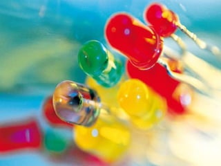
Light-emitting diodes
•
20 gostaram•12,769 visualizações

Basics of light-emitting diodes

Recomendados
Mais conteúdo relacionado
Mais procurados
Mais procurados (20)
Destaque
Destaque (20)
Semelhante a Light-emitting diodes
Semelhante a Light-emitting diodes (20)
Último
Último (20)
Light-emitting diodes
- 2. Yashpal Singh Katharria Semiconductor Light Emitting Diodes
- 3. History Captain Henry Joseph Round, England First observation of Electroluminescence from SiC crystals in the year 1907
- 4. History Captain Henry Joseph Round, England First observation of Electroluminescence from SiC crystals in the year 1907 Oleg Vladimirovich Losev, Imperial Russia Reported light emission from rectifier diode in 1927 A talented scientist who spent his life working as technician Published 43 articles in top Russian, British and German journals as a sole author and was granted 16 patents without getting any formal education Died in 1942 at the age of 39 during the blockade of Leningrad
- 5. History Captain Henry Joseph Round, England First observation of Electroluminescence from SiC crystals in the year 1907 Oleg Vladimirovich Losev, Imperial Russia Reported light emission from rectifier diode in 1927 A talented scientist who spent his life working as technician Published 43 articles in top Russian, British and German journals as a sole author and was granted 16 patents without getting any formal education Died in 1942 at the age of 39 during the blockade of Leningrad Nick Holonyak, GE New York, USA The father of the light-emitting diode: invented the first practically useful visible LED in 1962. His father worked in a coal-mine & he was the first member of his family to receive any formal schooling. First PhD student of John Bardeen
- 6. Shuji Nakamura, Nichia Corp., Japan Inventor of high-brightness GaN based LEDs P-type doping of GaN, high quality InGaN thin films, blue green, white LEDS and blue laser diodes The general conclusion among scientists at this time is that Dr. Nakamura’s inventions are so reliable and energy efficient that they are destined to replace Thomas Edison’s light bulb and save the world billions of dollars in energy costs. History
- 7. What is Light Emitting Diode (LED)? A device that converts electrical energy into Light A p-n junction diode that emits monochromatic light when forward biased. Requires 1.5 ~ 4 V and 10 mA to turn ON One needs to use a resistor to prevent overloading 10 V 0 V Symbol
- 8. How LED works? Ec Ev Eg e hole Ec Ev hn = Eg Semiconductors Indirect band gapDirect band gap Photon carries negligibly small momentum : p = h/l ...vertical transitions Indirect transitions: electron moving from CB to VB involves a phonon to satisfy momentum conservation; less probably transitions. Direct band gap : more light Indirect band gap : less light
- 9. How LED works? p-type (holes) n-type (electrons) Depletion region - - - - - - + + + p-n Junction p-type : holes and acceptors (-ive ions) n-type : electrons and donors (+ive ions) A region p-n junction is depleted of free carriers…Depletion Region (DR) Diffusion or built-in potential VD appears across DR.
- 10. How LED works? p-type (holes) n-type (electrons) Depletion region - - - - - - + + + hn Under forward bias; voltage drop across Depletion region Holes will move towards n-region Electrons towards p-region Carrier recombination can occurs in the depletion region and photons are emitted. Normally, Eg = hn However there are other situations like: - - - + + + EC EV ED EA EC EV EC EV hn1 hn2 hn3 Active region EA ED
- 11. Optical emission spectra of LED Dispersion curves for electrons and holes can be given by the following equations Energy of the emitted photon can be given by a joint dispersion relation Joint density of states will be given by The distribution of carriers in allowed bands is given by a Boltzman function
- 12. Optical emission spectra of LED The emission intensity as a function of energy I(E) = r(E) . FB(E) The maximum intensity occurs at
- 13. Ge Si GaAs Current-Voltage Characteristics For current flow through the junction Applied bias V = VD ~ Eg
- 14. Radiative transitions : a transition leading to the emission of a photon. Non-radiative transitions : no photon emission 1. Defects (dangling bonds, impurities, point defects such as vacancies, interstitials) related transitions are usually called Shockley-Read-Hall recombinations; Most active at the surface of the devices. 2. Auger transitions: Important mechanism in narrow band gap materials Radiative and Non-radiative transitions EC EV ED ED EC EV EC EV hn1 hn2 hn3
- 15. Answer: to reduce TIR… Why do we need the dome? Dome + -
- 16. Total Internal Reflection (TIR) For GaAs-air interface, C = 16o which means that much of the light suffers TIR. 16o LED
- 17. To solve the problem we could: Shape the surface of the semiconductor into a dome or hemisphere so that light rays strike the surface angles < C therefore does not experience TIR. But expensive and not practical to shape p-n junction with dome-like structure. Encapsulation of the semiconductor junction within a dome-shaped transparent plastic medium (an epoxy) that has refractive index higher than air and lower than that of the semiconductor. Solving TIR problem n Electrodes Electrodes pn junction Plastic dome p
- 18. Reabsorption problem Light emission takes place from depletion region (active region). However, the emitted light can be re-absorbed in p-type region because the band gap energy of p-type material is same the energy of the emitted photon. hn = Eg n-type p-type Dep. Region Metal-contact Solutions: 1. Thin p-layer : e can escape the p-region and recombine at surface non-radiatively. 2. Hetrostructure LED
- 19. Hetrostructure or Quantum-well LEDs Eg1 Eg2 Quantum well (QW) Quantum wells help in: Carrier confinement Tuning the wavelength of the emitted light GaN band gap ~ 3.4 eV InN band gap ~ 0.7 eV InxGa1-xN (0 < x <1) band gap : 0.7 – 3.4 eV Advantages (1) Do not suffer from poor surface conditions since the active region is not near the surface. (2) Increased carrier injection efficiency due to the low doping active layer. (3) The photons emitted are also not absorbed in the top or bottom region because the photon energy is smaller than the bandgap of the n- or p-region. 2eV1.4eV n-AlGaAs p-GaAs p-AlGaAs
- 20. Quantum-well LEDs However, LEDs with single QW show carrier overflow when currents injected in the LEDs are exceeded above a certain value. Therefore, multiple-QWs are, now a days, employed in GaN based visible and UV-light LEDs.
- 21. Other LED Problems n-type p-type Dep. Region Metal-contact 1. Reflection at top metal-semiconductor interface Minimized by small area of the metal contact 2. Absorption in the top metal contact Minimized by small area of the metal contact 3. Current crowding at the top contact Minimized by using Current spreading layers 4. Efficiency Droop No definite solution yet
- 22. 1. Quantum Efficiency (QE) Number of Photons emitted per injected electron. The active region of an ideal LED emits 1 photon per injected electron. Thus QE=1 for ideal LED 2. Internal quantum efficiency (IQE) Is defined by 3. Extraction Efficiency (EE) Number of photons extracted into free space per photon emitted from the active region. Photons emitted from active region should escape from LED. In an ideal LED, all the photons emitted from the active region are emitted into the free space. Therefore, EE=1 for ideal LED 4. External Quantum Efficiency (EQE) Is defined by Basic Terms
- 23. 5. Power Efficiency (or wall-plug efficiency) Is defined as I.V is power provided to the LED and P is output power. Basic Terms
- 24. Traffic signals, street light Residential Information boards Buildings Common application: Digital clock, battery level indicator, torch Outdoor: runway in airports Applications
- 25. Thank you very much for you attentions !! Any Questions??
- 27. • For now, between 25 & 50% efficiency, but some researchers think it’s possible to have 90% efficiency! Contrary to the traditional light bulb which has 5% efficiency and no perspective to do better!
- 28. Good efficiency & durability • LEDs can provide 50 000 hrs of life compared to 1000 hrs with incandescent light bulbs • Associated with perfect material and devices, LEDs would require only 3 Watts to generate the light obtained with a 60-Watt incandescent bulb LED vs. conventional light sources degradation in light output over time
- 29. Color Name Wavelength (Nanometers) Semiconductor Composition Infrared 880 GaAlAs/GaAs Ultra Red 660 GaAlAs/GaAlAs Super Red 633 AlGaInP Super Orange 612 AlGaInP Orange 605 GaAsP/GaP Yellow 585 GaAsP/GaP Incandescent White 4500K (CT) InGaN/SiC Pale White 6500K (CT) InGaN/SiC Cool White 8000K (CT) InGaN/SiC Pure Green 555 GaP/GaP Super Blue 470 GaN/SiC Blue Violet 430 GaN/SiC Ultraviolet 395 InGaN/SiC
- 31. • Similarities – Has anode and cathode • Electrons flow out through anode and in through cathode – Operates like diode; must be forward-biased – Photons are emitted when electrons fill holes in the emissive layer • Differences from conventional LED: – Emissive and conductive layers are organic compounds or polymers – Substrate can be plastic Similarities and differences between OLEDs and LEDs
- 32. 11 Environment Result doubly environment-friendly • Less current consumption (less electricity burned) • Less heat produced Less CO2 emissions Less light pollution Positive impact on global warming Incandescent traffic lights replaced by LEDs in USA: economy of 2.5 billion kWhours = US$ 200 million = 3 billion kilos of CO2 released in the atmosphere