Combinatorial approach to materials discovery.
•
1 gostou•3,206 visualizações

Plenary lecture of the XIV SBPMat Meeting, given by Prof. Ichiro Takeuchi (University of Maryland, USA) on September 30, 2015, in Rio de Janeiro (Brazil).

Recomendados
Recomendados
Mais conteúdo relacionado
Mais procurados
Mais procurados (20)
Destaque
Destaque (20)
Semelhante a Combinatorial approach to materials discovery.
Semelhante a Combinatorial approach to materials discovery. (20)
Mais de Sociedade Brasileira de Pesquisa em Materiais
Mais de Sociedade Brasileira de Pesquisa em Materiais (20)
Último
Último (20)
Combinatorial approach to materials discovery.
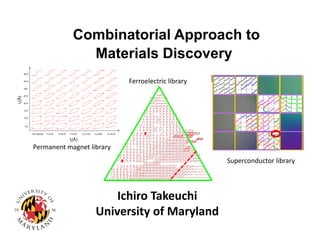
- 1. No impurity Ti (3 Å) Ti (6 Å) Ti (9 Å) Cu (3 Å) Cu (6Å) Cu (9 Å) 5 Å 10 Å 15 Å 20 Å 25 Å 35Å 45 Å 55 Å ti(Å) ts(Å) Permanent magnet library Ferroelectric library Superconductor library Ichiro Takeuchi University of Maryland Combinatorial Approach to Materials Discovery
- 2. • Introduction to the combinatorial approach: brief history, tools and strategies • Integrated materials discovery engine • Recent examples: combinatorial search of rare-earth-free permanent magnets; superconductors Outline
- 3. University of Maryland Tieren Gao Sean Fackler Kui Jin R. Greene SLAC A. Mehta US DOE, ONR, AFOSR Support Acknowledgement Duke University S. Curtarolo Ames Lab M. J. Kramer NIST A. G. Kusne M. Green
- 7. Combinatorial Libraries of Inorganic Materials Luminescent materials libraries, Science 279, 1712 (1998) Semiconductor gas sensor library, “electronic nose”, Appl. Phys. Lett. 83, 1255 (2003) Magnetic shape memory alloy library, Nature Materials 2, 180 (2003)
- 8. Fabrication of libraries and spreads Combinatorial PLD systems – metal oxides Combinatorial UHV sputtering system – metallic alloys Combinatorial multigun e-beam evaporator system – metal Combinatorial laser MBE – metal oxides Rapid characterization tools Scanning SQUID microscopes – magnetic properties Scanning microwave microscopes – resistive, magnetic, dielectric Scanning X-ray microdiffractometer Magneto-optical Kerr effect (MOKE) system – magnetic properties Scanning 4-point probe station – transport Novel device libraries incorporating MEMS, etc. Major Facilities for Combinatorial Materials Research at Maryland Focus: Functional Thin Film Materials
- 9. Correlation between materials complexity and physical properties Hg Nb3Ge La2CuO4 YBa2Cu3O7 HgBa2CaCu3O7 CriticalTemp.(K) 30 60 90 120 150 180 210 240 1 Number of Elements 2 3 4 5 6 7
- 10. 1 IA 2 IIA 3 IIIB 4 IVB 5 VB 6 VIB 7 VIIB 8 VIII 9 VIII 10 VIII 11 IB 12 IIB 13 IIIA 14 IVA 15 VA 16 VIA 17 VIIA 18 0 H1 He2 Li 3 Be 4 B 5 C 6 N 7 O 8 F 9 Ne 10 Na 11 Mg 12 Al 13 Si 14 P 15 S 16 Cl 17 Ar 18 K 19 Ca 20 Sc 21 Ti 22 V 23 Cr 24 Mn 25 Fe 26 Co 27 Ni 28 Cu 29 Zn 30 Ga 31 Ge 32 As 33 Se 34 Br 35 Kr 36 Rb 37 Sr 38 Y 39 Zr 40 Nb 41 Mo 42 Tc 43 Ru 44 Rh 45 Pd 46 Ag 47 Cd 48 In 49 Sn 50 Sb 51 Te 52 I 53 Xe 54 Cs 55 Ba 56 La 57 Hf 72 Ta 73 W 74 Re 75 Os 76 Ir 77 Pt 78 Au 79 Hg 80 Tl 81 Pb 82 Bi 83 Po 84 At 85 Rn 86 Fr 87 Ra 88 Ac 89 Unq 104 Unp 105 Unh 106 Uns 107 Uno 108 Une 109 Uun 110 Ce 58 Pr 59 Nd 60 Pm 61 Sm 62 Eu 63 Gd 64 Tb 65 Dy 66 Ho 67 Er 68 Tm 69 Yb 70 Lu 71 Th 90 Pa 91 U 92 Np 93 Pu 94 Am 95 Cm 96 Bk 97 Cf 98 Es 99 Fm 100 Md 101 No 102 Lr 103 Binary compounds have the form AB. (e. g., MgF, SiC, ZnO,…..) 60 x 59 x different combinations: most are known. Ternary compounds have the form ABC. (BaTiO, NiMnGa, HgCdTe,…) 60 x 59 x 58 x different combinations: ~3 % of all possible known Quaternary compounds have the form ABCD. (YBaCuO, AlNiCOFe,…) 60 x 59 x 58 x 57 x different combinations: 0.01% of all possible known Beyond?? How many different compounds are there? Take 60 “useful” elements. There are about ~100,000 known inorganic compounds.
- 13. Ba Quaternary Masking: 1st mask, 1st position
- 14. Ca Quaternary Masking: 1st mask, 2nd position
- 15. Sr Quaternary Masking: 1st mask, 3rd position
- 16. Pb Quaternary Masking: 1st mask, 4th position
- 17. BaPb Sr Ca Ba Quaternary Masking: after 1st mask
- 18. BaPb Sr Ca Ba Zr Zr Zr Zr Quaternary Masking: 2nd mask, 1st position
- 19. BaPb Sr Ca Ba Ta Ta Ta Ta Quaternary Masking: 2nd mask, 2nd position
- 20. BaPb Sr Ca Ba Nb Nb Nb Nb Quaternary Masking: 2nd mask, 3rd position
- 21. BaPb Sr Ca Ba Ti Ti Ti Ti Quaternary Masking: 2nd mask, 4th position
- 23. A B C ED # depositions: 4 x n # combinations: 4n 5 masks: 4 x 5 = 20 depo’s 45 = 1024 samples
- 24. (Right) Luminescent image of the same library after thermally processed under UV excitation. Science 279, 1712 (1998) Library of luminescent materials made w/ quaternary masking
- 25. Various combinatorial experimental designs: discrete libraries vs composition spreads Composition A B B A C • Composition spreads allow continuous mapping of physical properties and phase boundaries • Run to run variation in ordinary experiments is removed
- 27. Fabrication of epitaxial composition spread of oxides via laser MBE
- 28. Takeuchi et al., Applied Physics Letters 79, 4411 (2001) Scanning Microwave Microscope: a rapid characterization tool Originally developed for rapid screening of libraries of superconductors, dielectric materials, etc. SampleTip Coaxial ¼ resonator x-y-z stage Motion controller Computer f0 Q Microwave source Review Article: Gao, et al., Measurement Science and Technology 16, 248 (2005)
- 29. -250 -200 -150 -100 -50 0 50 100 150 200 880 890 900 910 920 930 940 950 960 970 Magnetic field (Oe) FMRsignal(arb.unit) 2.45 GHz SrTiO3 BaTiO3 CaTiO3 500 400 100 300 0 200 r Different physical properties can be mapped using an existing microwave microscope Dielectric constant mapping of a (Ba,Sr,Ca)TiO3 pseudo- ternary library at 1 GHz Appl. Phys. Lett. 74, 1165 (1999) Ferromagnetic resonance (FMR) signal taken at a spot Dielectric property Magnetic property (spin resonance) composition plot
- 30. Mode/materials [reference] Physical parameter/ phenomenon Spatial resolution Dielectric [12-14] Complex dielectric constant 100 nm Metal [13] Impedance/resistivity 100 nm Non-linear dielectric [15,18] Non-linear dielectric constant 1 nm FMR Ferromagnetic resonance 100 nm* STM-ESR Electron spin resonance Atomic resolution Capabilities of Multiscale Microwave Microscope Mapping of various physical properties can be obtained at macroscopic scale (~ 1 cm) down to the listed spatial resolution
- 32. Composition Spreads of Ternary Metallic Alloy Systems Co-sputtering scheme Ni Mn Al 3” spread wafer Ni Al Mn Phase diagram Composition is mapped using an electron probe (WDS)
- 33. RT Scanning SQUID microscope (Magma, Neocera) SQUID assembly inside vacuum leveling probe and scanning stage Room temperature samples are measured z-SQUID is used to measure Bz distribution Tip-sample distance is typically 100~200 microns
- 34. 15 20 25 30 35 40 45 50 60 50 40 30 20 col row -2.50e+007 0.00e+000 2.50e+007 rho1_25_x 100-150 emu/cc 50-70 emu/cc 30-40 emu/cc 10-20 emu/cc Scanning SQUID image of a Ni-Mn-Ga spread wafer (room temperature) 0 13 25 38 50 63 75 80 60 40 20 0 col row -2.50e+007 0.00e+000 2.50e+007 rho1_25 Mn rich Ni rich Ni2Ga3 rich
- 35. Combinatorial Search of Ferromagnetic Materials Ga Ni 0 1 2 3 4 5 6 7 8 9 10 Mn 50 100 150 200 250 M (emu/cc) Ni2Ga3 Nature Materials 2, 180 (2003)
- 36. Rapid detection of shape memory alloy compositions by visual inspection Composition spread deposited on micromachined cantilever array Film thickness ~0.5 m Detection of martensitic phase transformation
- 37. Functional phase diagram of Ni-Mn-Ga 20 40 80 20 40 60 80 60 80 20 Mn 40 20 40 80 20 40 60 80 Ni 60 80 20 40 Ni2Ga3 Ga Increasing transition temperature Ferromagnetic regions Most strongly magnetic Martensites Nature Materials 2, 180 (2003)
- 38. Integration of theory and high-throughput experiments Step 2 Step 3Step 1 Integrated materials discovery engine Experimental Track Theoretical Track
- 39. Step 2 Step 3Step 1 Experimental Track Theoretical Track Advantages of this approach: Predictions are sometimes “off” by stoichiometric variations. Integration of theory and high-throughput experiments
- 40. Step 2 Step 3Step 1 Experimental Track Theoretical Track Advantages of this approach: Predictions are sometimes “off” by stoichiometric variations. Large number of data points in combinatorial experiments suitable for building models. Integration of theory and high-throughput experiments
- 42. Step 2 Step 3Step 1 Experimental Track Theoretical Track Example: Rare‐earth‐free permanent magnets APL 102, 022419 (2013); Scientific Reports 4, 6367 (2014) Integration of theory and high-throughput experiments
- 43. Rare-earth (Nd, Dy, Sm, etc.)-free magnets are needed due to their fluctuating prices Search for new permanent magnet materials w/o rare-earth elements The prices of many rare‐earth metals have increased by more than 10 fold in the past few years Permanent magnets for: direct drive wind turbines Current magnets: Nd‐Fe‐B, Sm‐Co Advanced electric drive motors
- 44. History of development of permanent magnets Best magnets contain rare-earth elements: Nd, Dy, Sm Nd-Fe-B Sm-Co Year
- 45. How to design new permanent magnets • Need high energy product (BH)max • Need high magnetization M ‐ need Fe and/or Co • Need high uniaxial anisotropy K – coercive field Hc ‐ e.g. NdFeB: 5 x 10⁶ J/m3; SmCo5 2 x 10⁷ J/m3 Paths to intrinsic anisotropy (without rare‐earth): • Modify FeCo: cubic to tetragonal, electronic structure • MnBi/MnAlX • Atomically ordered phase of FeNi
- 46. Modify/distort FeCo: add 3rd element X (d elements): spin‐orbit coupling; high anisotropy high coercive field ‐> Make Fe‐Co‐X composition spreads 1852 C 2150 C 3412 C 2617 C Melting points Melting points 1536 C 1495 C
- 48. Hc ~ 1.2 KOe (K ~ 30 eV/atom) Hc mapping Grouping of structures based on synchrotron diffraction Fe Mo Co Identification of composition with enhanced coercive field: Fe‐Co‐Mo Identification of composition with enhanced coercive field: Fe‐Co‐Mo Scientific Reports 4, 6367 (2014) Identified Fe8CoMo has a tetragonal structure; genetic algorithm and DFT give K values in agreement with experiment
- 49. Search for rare‐earth free permanent magnets • High energy product (BH)max ‐ High magnetization M (Fe and/or Co) ‐ High uniaxial anisotropy K – coercive field Hc (NdFeB: 5 x 10⁶ J/m3; SmCo5 2 x 10⁷ J/m3) Paths to intrinsic anisotropy (without rare‐earth): • Modify FeCo: cubic to tetragonal, electronic structure • MnBi/FeCo • Atomically ordered phase of FeNi
- 52. History of development of permanent magnets Nd-Fe-B Sm-Co Year This work: MnBi thin film/multilayers
- 53. Step 2 Step 3Step 1 Experimental Track Theoretical Track Examples: Combinatrorial search of superconductivity in Fe‐B APL Materials 1, 042101 (2013) Integration of theory and high-throughput experiments
- 54. Targeting superconductors predicted by theory Prediction: FeB4 is a superconductor with Tc ~ 15‐20 K
- 55. Fe-B phase diagram (1994) FeB2FeB4 Not much is known in this region
- 56. Exploration of new superconductors: Fe-B composition spread 3” wafer Fe rich B rich 16 spot 4‐terminal pogo pin arrays: Cut wafers into 1 cm2 pieces and measure 16 spots at once Color change tracks: composition change, crystallinity change, and metal to insulator transition
- 57. Fe-B composition spread: Fe-rich side, 16 spots on one 1 cm2 chip Ch 113” wafer more Bmore Fe temperature resistance 4.2 K 300 K All metallic
- 58. Semiconducting to insulating more Bmore Fe temperature resistance 4.2 K 300 K Fe-B composition spread: B-rich side, 16 spots on one 1 cm2 chip
- 59. Ch 11 Ch 3 Ch 13 Middle region: FeB2 – FeB4 more Bmore Fe temperature resistance 4.2 K 300 K Fe-B composition spread: FeBx(x =2-4), 16 spots on one 1 cm2 chip
- 60. FeBx: we have found the superconductor Susceptibility shows diamagnetism Bc2(T)= Bc2(0)[1-(T/Tc)2]/ [1+(T/Tc)2] gives Bc2(0) = 2 T -> Type II BCS superconductor Partial R drop ~ 10 K? Superconducting phase was detected in 2 spread wafers
- 61. Combinatorial Time Lapse: a day in the life of a combinatorial materials scientist Sean Fackler