SlideShare uma empresa Scribd logo
1 de 13
ARM – ADVANCED RISC MACHINE (LPC 2148)
The LPC2148 microcontrollers are based on a 32 bit ARM7TDMI-S CPU with real-
time emulation and embedded trace support, that combines the microcontroller with
embedded high speed flash memory ranging from 32 kB to 512 kB. A 128-bit wide memory
interface and unique accelerator architecture enable 32-bit code execution at the maximum
clock rate. For critical code size applications, the alternative 16-bit Thumb mode reduces
code by more than 30 % with minimal performance penalty.
Due to the tiny size and low power consumption, LPC2148 is ideal for applications
where miniaturization is a key requirement, such as access control and point-of-sale. A blend
of serial communications interfaces ranging from a USB 2.0 Full Speed device, multiple
UARTs, SPI, SSP to I2Cs, and on-chip SRAM of 8 kB up to 40 kB, make these devices very
well suited for communication gateways and protocol converters, soft modems, voice
recognition and low end imaging, providing both large buffer size and high processing
power. Various 32-bit timers, single or dual 10-bit ADC(s), 10-bit DAC, PWM channels and
45 fast GPIO lines with up to nine edge or level sensitive external interrupt pins make these
microcontrollers particularly suitable for industrial control and medical systems.
FEATURES
 16/32-bit ARM7TDMI-S microcontroller in a tiny LQFP64 package.
 8 to 40 KB of on-chip static RAM and 32 to 512 KB of on-chip flash program
memory.
 128 bit wide interface/accelerator enables high speed 60 MHz operation.
 In-System/In-Application Programming (ISP/IAP) via on-chip boot-loader software.
Single flash sector or full chip erase in 400 ms and programming of 256 bytes in 1 ms.
 USB 2.0 Full Speed compliant Device Controller with 2 KB of endpoint RAM.
 In addition, LPC2148 provides 8 KB of on-chip RAM accessible to USB by DMA.
 Two 10-bit A/D converters provide a total of 6/14 analog inputs, with conversion
times as low as 2.44 micros per channel.
 Single 10-bit D/A converter provides variable analog output.
 Two 32-bit timers/external event counters (with four captures and four compare
channels each), PWM unit (six outputs) and watchdog.
 Low power real-time clock with independent power and dedicated 32 kHz clock
input.
 Multiple serial interfaces including two UARTs (16C550), two Fast I2C-buses
 (400 Kbit/s), SPI and SSP with buffering and variable data length capabilities.
 Vectored interrupt controller with configurable priorities and vector addresses.
 Up to 45 of 5 V tolerant fast general purpose I/O pins in a tiny LQFP64 package.
 Up to nine edge or level sensitive external interrupt pins available.
4.1.1 ARCHITECTURAL OVERVIEW
The LPC2148 consists of an ARM7TDMI-S CPU with emulation support, the ARM7
Local Bus for interface to on-chip memory controllers, the AMBA Advanced High-
performance Bus (AHB) for interface to the interrupt controller, and the ARM Peripheral Bus
(APB, a compatible superset of ARM’s AMBA Advanced Peripheral Bus) for connection to
on-chip peripheral functions. The LPC2148 configures the ARM7TDMI-S processor in little-
endian byte order. AHB peripherals are allocated a 2 megabyte range of addresses at the very
top of the 4 gigabyte ARM memory space. Each AHB peripheral is allocated a 16 kB address
space within the AHB address space. LPC2148 peripheral functions (other than the interrupt
controller) are connected to the APB bus. The AHB to APB bridge interfaces the APB bus to
the AHB bus. APB peripherals are also allocated a 2 megabyte range of addresses, beginning
at the 3.5 gigabyte address point. Each APB peripheral is allocated a 16 kB address space
within the APB address space. The connection of on-chip peripherals to device pins is
controlled by a Pin Connect Block. This must be configured by software to fit specific
application requirements for the use of peripheral functions and pins.
FIG 4.1- Block Diagram of LPC 2148
4.1.2 ARM7TDMI-S PROCESSOR
The ARM7TDMI-S is a general purpose 32-bit microprocessor, which offers high
performance and very low power consumption. The ARM architecture is based on Reduced
Instruction Set Computer (RISC) principles, and the instruction set and related decode
mechanism are much simpler than those of micro programmed Complex Instruction Set
Computers. This simplicity results in a high instruction throughput and impressive real-time
interrupt response from a small and cost-effective processor core. Pipeline techniques are
employed so that all parts of the processing and memory systems can operate continuously.
Typically, while one instruction is being executed, its successor is being decoded, and a third
instruction is being fetched from memory. The ARM7TDMI-S processor also employs a
unique architectural strategy known as THUMB, which makes it ideally suited to high-
volume applications with memory restrictions or applications where code density is an issue.
The key idea behind THUMB is that of a super-reduced instruction set. Essentially, the
ARM7TDMI-S processor has two instruction sets:
• The standard 32-bit ARM instruction set.
• A 16-bit THUMB instruction set.
The THUMB set’s 16-bit instruction length allows it to approach twice the density of
standard ARM code while retaining most of the ARM’s performance advantage over a
traditional 16-bit processor using 16-bit registers. This is possible because THUMB code
operates on the same 32-bit register set as ARM code. THUMB code is able to provide up to
65% of the code size of ARM, and 160% of the performance of an equivalent ARM
processor connected to a 16-bit memory system.
4.1.3 Description about the Block Diagram:
On chip Flash Program Memory
LPC 2148 is having 512 k B Flash memory. This memory may be used for both code
and data storage. Programming of the flash memory may be accomplished in several ways
(ISP/IAP).
On chip Static RAM
On-chip static RAM may be used for code and/or data storage. The SRAM may be
accessed as 8-bit, 16-bit, and 32-bit. An 8 k B SRAM block intended to be utilized mainly by
the USB
Interrupt Controller
The Vectored Interrupt Controller (VIC) accepts all of the interrupt request inputs and
categorizes them as Fast Interrupt Request (FIQ), vectored Interrupt Request (IRQ), and non-
vectored IRQ as defined by programmable settings.
Analog to Digital Converter
LPC2148 contains two analog to digital converters (ADC0 & ADC1). Total number
of available ADC inputs is 14. These two ADC’s are 10 bit successive approximation analog
to digital converters. The measurement range is 0 V to VREF and is Global Start command for
both converters.
Digital to Analog Converter
The DAC enables to generate a variable analog output. The maximum DAC output
voltage is the VREF voltage. 10-bit DAC, Buffered output and Power-down mode are
available.
USB 2.0 Device Controller
The USB is a 4-wire serial bus that supports communication between a host and a
number (127max) of peripherals. This enables 12 M bit/s data exchange with a USB host
controller. A DMA controller (available only in LPC2146/48) can transfer data between an endpoint
buffer and the USB RAM.
UART
LPC2148 contains two UARTs (UART0 & UART1). In addition to standard transmit
and receive data lines, the LPC2148 UART1 also provide a full modem control handshake
interface. 16 byte Receive and Transmit FIFOs are used. It contains Built-in fractional baud
rate generator covering wide range of baud rates without a need for external crystals of
particular values.
I2C-bus serial I/O controller
I2C is a bidirectional. It is a multi-master bus; it can be controlled by more than one
bus master connected to it. It supports bit rates up to 400 k bit/s. Bidirectional data transfer
between masters and slaves. Serial clock synchronization allows devices with different bit
rates to communicate via one serial bus. Serial clock synchronization can be used as a
handshake mechanism to suspend and resume serial transfer.
SPI serial I/O control
It is s a full duplex serial interface, designed to handle multiple masters and slaves
connected to a given bus. Synchronous, Serial, Full Duplex Communication is considered in
the system.
SSP serial I/O control:-
Supports full duplex transfers. Data frames of 4 bits to 16 bits of data flowing from
the master to the slave and from the slave to the master. Synchronous serial communication
Master or slave operation. 8-frame FIFOs for both transmit and receive. Four bits to 16 bits
per frame
Timers
LPC 2148 has two 32-bit timer/counters with a programmable 32-bit pre scalar. It also
having external event counter. Four 32-bit capture channels per timer/counter that can take a
snapshot of the timer value when an input signals transitions. A capture event may also
optionally generate an interrupt..
Watchdog Timer
The purpose of the watchdog is to reset the microcontroller within a reasonable
amount of time if it enters an erroneous state. When enabled, the watchdog will generate a
system reset if the user program fails to ‘feed’ (or reload) the watchdog within a
predetermined amount of time.
Real Time Clock
The RTC is designed to provide a set of counters to measure time when normal or idle
Operating mode is selected. The RTC has been designed to use little power, making it
Suitable for battery powered systems where the CPU is not running continuously (Idle
Mode).
Crystal Oscillator
On-chip integrated oscillator operates with external crystal in range of 1 MHz to 25 M
Hz. The oscillator output frequency is called foscand the ARM processor clock frequency is
referred to as CCLK for purposes of rate equations, etc. fosc and CCLK are the same value
unless the PLL is running and connected.
PLL
The PLL accepts an input clock frequency in the range of 10 MHz to 25 MHz’s The
input frequency is multiplied up into the range of 10 MHz to 60 MHz with a Current
Controlled Oscillator (CCO). The multiplier can be an integer value from 1 to 32 (in practice,
the multiplier value cannot be higher than 6 on this family of microcontrollers due to the
upper frequency limit of the CPU). The CCO operates in the range of 156 MHz to 320 MHz,
so there is an additional divider in the loop to keep the CCO within its frequency range while
the PLL is providing the desired output frequency.
4.1.4 LPC 2148 REGISTERS
The ARM CPU provides in user mode 16 general purpose registers (R0 - R15) and a
Program Status Register. Registers in LPC 2148 are 8, 16 or 32 bits wide. The ARM CPU
provides shadow registers which are selected on an Operation Mode switch. These shadow
registers reduce interrupt latency. All CPU Registers are shown in the following picture.
SP: Stack pointer
LR: Link register
PC: Program counter
CPSR: Current Program Status Register.
SPSR: Saved Program Status Register.
Fig 4.2: Registers
LR (Link register): Used by the processor when there is a branch operation this occurs due
to function call or due to some condition checking. When the processor is executing and there
is a need to branch to other location the return address (the address from where the execution
is to be started, returning after completing the function execution). If there are multiple
function calls then LR will store only the last address before jumping.
CPSR: Used to store the important back-up data whenever there is change of any mode. E.g.
if the processor is executing user mode and there is an interrupt, before going to service the
interrupt the all the data and the status registers and the current mode of operation
information is stored in CPSR. CPSR registers are present in all the 7 modes but are not
usually shown.
SPSR: stores the copy of CPSR register in which ever mode the processor enters. All the 7
modes have SPSR registers and are shown in the mode registers. If the processor switches
from USER mode to IRQ mode because of an IRQ, the CPSR value is updated in the user
mode and the processor switches to IRQ mode. Beforestarting the IRQ code execution the
value of CPSR is copied to SPSR of IRQ mode. While executing IRQ mode and high priority
interrupt occurs (FIQ) then the status of the IRQ mode is updated in its CPSR register and
when the processor switches to FIQ mode the contents of CPSR in IRQ mode is copied to
SPSR register in FIQ mode.
4.1.5 General Purpose Input/output ports (GPIO)
Every physical GPIO port is accessible either the group of registers by providing an
enhanced features and accelerated port access or the legacy group of registers.
• Accelerated GPIO functions:
– GPIO registers are relocated to the ARM local bus so that the fastest possible I/O Timing
can be achieved.
– Mask registers allow treating sets of port bits as a group, leaving other bits Unchanged.
– All registers are byte and half-word addressable.
– Entire port value can be written in one instruction.
• Bit-level set and clear registers allow a single instruction set or clear of any number of bits
in one port.
• Direction control of individual bits.
• All I/O default to inputs after reset.
• Backward compatibility with other earlier devices is maintained with legacy registers
appearing at the original addresses on the VPB bus.
Applications:
• General purpose I/O
• Driving LEDs, or other indicators
• Controlling off-chip devices
• Sensing digital inputs
4.1.6 Pin Description
IOPIN: The current state of the GPIO configured port pins can always be read from this
register, regardless of pin direction.
IOSET: This register controls the state of output pins in conjunction with the IOCLR
register. Writing one’s produces highs at the corresponding port pins. Writing zeroes has no
effect.
IODIR: GPIO Port Direction control register: This register individually controls the
direction of each port pin. Direction bit for any pin must be set according to the pin
functionality.
IOCLR: GPIO Port Output Clear register: This register controls the state of output pins.
Writing ones produces lows at the corresponding port pins and clears the corresponding bits
in the IOSET register. Writing zeros has no effect.
4.1.7 PIN diagram of LPC 2148
Fig 4.3:Pin diagram of LPC 2148
EXTERNAL INTERRUPT INPUTS
The LPC 2148 includes four External Interrupt Inputs as selectable pin functions. The
External Interrupt Inputs can optionally be used to wake up the processor from the Power
Down mode.
REGISTER DESCRIPTION
The external interrupt function has four registers associated with it. The EXTINT
register contains the interrupt flags, and the EXTWAKEUP register contains bits that enable
individual external interrupts to wake up the LPC 2148 from Power Down mode. The
EXTMODE and EXTPOLAR registers specify the level and edge sensitivity parameters.
External Interrupt Flag Register
When a pin is selected for its external interrupt function, the level or edge on that pin
selected by its bits in the EXTPOLAR and EXTMODE registers will set its interrupt flag in
this register. This asserts the corresponding interrupt request to the VIC, which will cause an
interrupt if interrupts from the pin are enabled. Writing ones to bits EINT0 through EINT3 in
EXTINT register clears the corresponding bits. In level-sensitive mode this action is
efficacious only when the pin is in its inactive state.
4.1.8 UART0
FEATURES
• 16 byte Receive and Transmit FIFO.
• Register locations conform to ‘550 industry standard.
• Receiver FIFO triggers points at 1, 4, 8, and 14 bytes.
• Built-in baud rate generator.
UART PIN DESCRIPTION
Table 4.1: UART PIN description
There are two Universal Asynchronous Receiver Transmitters (UART) configured in
ARM 7-LPC 2148 viz. UART-0 and UART -1.Register which are related for UART
configurations are UO/1LCR, UO/1THR, UO/1RBR and UO/1LSR.
LCR: Line Control Register.
THR: Transmit Holding Register.
RBR: Receive Buffer Register.
LSR: Line Status Register.
UO/1LSR –
7 6 5 4 3 2 1 0
Divisor
latch bit
UART
trans
enb/disable
Odd/even
parity
Enable
/disable
Parity Bit
Stop
Bit
Width of data
Recvd& trans.
Bits 1:0-
‘0 0 ‘- 5 bit data.
‘0 1- 6 bit data.
‘1 0 -7 bit data.
‘1 1’- 8 bit data.
Bit 2:
‘0’ - 1 stop bit.
‘1’ - 2 stop bits.
Bit 3:
‘0’ - Disable parity bit.
‘1’ - Enable parity bit.
Bits 4:5 :
‘0 0’ - odd parity.
‘0 1’ – even parity.
Bit 6:
‘0’ - Enable transmission bit.
‘1’ - Disable transmission bit.
Bit- 7:
‘1’ - to set baud rate.
To set baud rate two registers UO/1DLL (Divisor Latch LSB) and U0/1DLM (Divisor Latch
MSB) are used.
Baud rate value = Processor clock frequency
16* Baud rate (in bits per sec)
U0/1LSR: (status of UART)
7 6 5 4 3 2 1 0
X X TRANS STATUS X X X X RECEIV
STATUS
U0/1THR: Data that is transmitted will be available in U0/1THR and then sent to other
registers.
U0/1RBR: Data that is received will be available in U0/1THR and then sent to other
registers.

Mais conteúdo relacionado

Mais procurados

Jtag presentation
Jtag presentationJtag presentation
Jtag presentation
klinetik
 
I2C And SPI Part-23
I2C And  SPI Part-23I2C And  SPI Part-23
I2C And SPI Part-23
Techvilla
 

Mais procurados (20)

ATM
ATMATM
ATM
 
Embedded system in Smart Cards
Embedded system in Smart CardsEmbedded system in Smart Cards
Embedded system in Smart Cards
 
I2C
I2CI2C
I2C
 
Watch-dog Timer in LPC1768
Watch-dog Timer in LPC1768Watch-dog Timer in LPC1768
Watch-dog Timer in LPC1768
 
Design for Testability
Design for Testability Design for Testability
Design for Testability
 
I2C Protocol
I2C ProtocolI2C Protocol
I2C Protocol
 
Architecture of 8051
Architecture of 8051Architecture of 8051
Architecture of 8051
 
Serial Data Communication
Serial Data CommunicationSerial Data Communication
Serial Data Communication
 
8051 MICROCONTROLLER
8051 MICROCONTROLLER 8051 MICROCONTROLLER
8051 MICROCONTROLLER
 
Embedded systems and its ports
Embedded systems and its portsEmbedded systems and its ports
Embedded systems and its ports
 
INTERRUPTS OF 8086 MICROPROCESSOR
INTERRUPTS OF 8086 MICROPROCESSORINTERRUPTS OF 8086 MICROPROCESSOR
INTERRUPTS OF 8086 MICROPROCESSOR
 
Interfacing LCD with 8051 Microcontroller
Interfacing LCD with 8051 MicrocontrollerInterfacing LCD with 8051 Microcontroller
Interfacing LCD with 8051 Microcontroller
 
Minimum mode and Maximum mode Configuration in 8086
Minimum mode and Maximum mode Configuration in 8086Minimum mode and Maximum mode Configuration in 8086
Minimum mode and Maximum mode Configuration in 8086
 
System verilog important
System verilog importantSystem verilog important
System verilog important
 
I2C Protocol
I2C ProtocolI2C Protocol
I2C Protocol
 
Uart
UartUart
Uart
 
Level sensitive scan design(LSSD) and Boundry scan(BS)
Level sensitive scan design(LSSD) and Boundry scan(BS)Level sensitive scan design(LSSD) and Boundry scan(BS)
Level sensitive scan design(LSSD) and Boundry scan(BS)
 
Jtag presentation
Jtag presentationJtag presentation
Jtag presentation
 
I2C And SPI Part-23
I2C And  SPI Part-23I2C And  SPI Part-23
I2C And SPI Part-23
 
Device drivers and interrupt service mechanism
Device drivers and interrupt service mechanismDevice drivers and interrupt service mechanism
Device drivers and interrupt service mechanism
 

Destaque

poka yoke seminar report with index
poka yoke seminar report with indexpoka yoke seminar report with index
poka yoke seminar report with index
N Harisha
 
Digital Notice Board
Digital Notice BoardDigital Notice Board
Digital Notice Board
Raaki Gadde
 

Destaque (20)

Raspberry Pi
Raspberry PiRaspberry Pi
Raspberry Pi
 
poka yoke seminar report with index
poka yoke seminar report with indexpoka yoke seminar report with index
poka yoke seminar report with index
 
Arm7 architecture
Arm7 architectureArm7 architecture
Arm7 architecture
 
Harisha
HarishaHarisha
Harisha
 
Coin Based Water Flow System Using ARM7(LPC2148) By Nehad
Coin Based Water Flow System Using ARM7(LPC2148) By NehadCoin Based Water Flow System Using ARM7(LPC2148) By Nehad
Coin Based Water Flow System Using ARM7(LPC2148) By Nehad
 
Getting Started with Raspberry Pi v1.2
Getting Started with Raspberry Pi v1.2Getting Started with Raspberry Pi v1.2
Getting Started with Raspberry Pi v1.2
 
POKA-YOKE REPORT IN PDF FORM
POKA-YOKE REPORT IN PDF FORMPOKA-YOKE REPORT IN PDF FORM
POKA-YOKE REPORT IN PDF FORM
 
Raspberry Pi Technology
Raspberry Pi TechnologyRaspberry Pi Technology
Raspberry Pi Technology
 
Introduction To Raspberry Pi with Simple GPIO pin Control
Introduction To Raspberry Pi with Simple GPIO pin ControlIntroduction To Raspberry Pi with Simple GPIO pin Control
Introduction To Raspberry Pi with Simple GPIO pin Control
 
Raspberry pi technology
Raspberry pi technologyRaspberry pi technology
Raspberry pi technology
 
Lidar technology and it’s applications
Lidar technology and it’s applicationsLidar technology and it’s applications
Lidar technology and it’s applications
 
Raspberrypi workshop outline
Raspberrypi workshop outlineRaspberrypi workshop outline
Raspberrypi workshop outline
 
Raspberrypi
RaspberrypiRaspberrypi
Raspberrypi
 
Arm
ArmArm
Arm
 
Seminar ppt
Seminar pptSeminar ppt
Seminar ppt
 
Introduction to Raspberry Pi and GPIO
Introduction to Raspberry Pi and GPIOIntroduction to Raspberry Pi and GPIO
Introduction to Raspberry Pi and GPIO
 
ARM lab programs
ARM  lab programs  ARM  lab programs
ARM lab programs
 
Spi in arm7(lpc2148)
Spi in arm7(lpc2148)Spi in arm7(lpc2148)
Spi in arm7(lpc2148)
 
Raspberry Pi 3 Latest PPT - Robomart
Raspberry Pi 3 Latest PPT - RobomartRaspberry Pi 3 Latest PPT - Robomart
Raspberry Pi 3 Latest PPT - Robomart
 
Digital Notice Board
Digital Notice BoardDigital Notice Board
Digital Notice Board
 

Semelhante a Arm7 document

Lpc1769 68 67_66_65_64
Lpc1769 68 67_66_65_64Lpc1769 68 67_66_65_64
Lpc1769 68 67_66_65_64
trowftd
 
AN INTEGRATED FOUR-PORT DC-DC CONVERTER-CEI0080
AN INTEGRATED FOUR-PORT DC-DC CONVERTER-CEI0080AN INTEGRATED FOUR-PORT DC-DC CONVERTER-CEI0080
AN INTEGRATED FOUR-PORT DC-DC CONVERTER-CEI0080
Vivek Venugopal
 

Semelhante a Arm7 document (20)

An Overview of LPC2101/02/03
An Overview of LPC2101/02/03An Overview of LPC2101/02/03
An Overview of LPC2101/02/03
 
Digital electronics
Digital electronicsDigital electronics
Digital electronics
 
Lpc1769 68 67_66_65_64
Lpc1769 68 67_66_65_64Lpc1769 68 67_66_65_64
Lpc1769 68 67_66_65_64
 
Arm usr m,anl
Arm usr m,anlArm usr m,anl
Arm usr m,anl
 
Pic microcontrollers
Pic microcontrollersPic microcontrollers
Pic microcontrollers
 
LPC 2148 ARM MICROCONTROLLER
LPC 2148 ARM MICROCONTROLLERLPC 2148 ARM MICROCONTROLLER
LPC 2148 ARM MICROCONTROLLER
 
Overview of LPC213x MCUs
Overview of LPC213x MCUsOverview of LPC213x MCUs
Overview of LPC213x MCUs
 
PIC32MX5XX/6XX/7XX USB, CAN and Ethernet 32-Bit Flash Microcontrollers
PIC32MX5XX/6XX/7XX USB, CAN and Ethernet 32-Bit Flash MicrocontrollersPIC32MX5XX/6XX/7XX USB, CAN and Ethernet 32-Bit Flash Microcontrollers
PIC32MX5XX/6XX/7XX USB, CAN and Ethernet 32-Bit Flash Microcontrollers
 
Unit II Study of Onchip Peripherals
Unit II Study of Onchip PeripheralsUnit II Study of Onchip Peripherals
Unit II Study of Onchip Peripherals
 
Introducing OMAP-L138/AM1808 Processor Architecture and Hawkboard Peripherals
Introducing OMAP-L138/AM1808 Processor Architecture and Hawkboard PeripheralsIntroducing OMAP-L138/AM1808 Processor Architecture and Hawkboard Peripherals
Introducing OMAP-L138/AM1808 Processor Architecture and Hawkboard Peripherals
 
Overview of LPC214x MCUs
Overview of LPC214x MCUsOverview of LPC214x MCUs
Overview of LPC214x MCUs
 
Doc32059
Doc32059Doc32059
Doc32059
 
32059 sistem
32059 sistem32059 sistem
32059 sistem
 
PIC MICROCONTROLLERS -CLASS NOTES
PIC MICROCONTROLLERS -CLASS NOTESPIC MICROCONTROLLERS -CLASS NOTES
PIC MICROCONTROLLERS -CLASS NOTES
 
Study on 32-bit Cortex - M3 Powered MCU: STM32F101
Study on 32-bit Cortex - M3 Powered MCU: STM32F101Study on 32-bit Cortex - M3 Powered MCU: STM32F101
Study on 32-bit Cortex - M3 Powered MCU: STM32F101
 
AN INTEGRATED FOUR-PORT DC-DC CONVERTER-CEI0080
AN INTEGRATED FOUR-PORT DC-DC CONVERTER-CEI0080AN INTEGRATED FOUR-PORT DC-DC CONVERTER-CEI0080
AN INTEGRATED FOUR-PORT DC-DC CONVERTER-CEI0080
 
Introduction to i.MX27 Multimedia Applications Processors
Introduction to i.MX27 Multimedia Applications ProcessorsIntroduction to i.MX27 Multimedia Applications Processors
Introduction to i.MX27 Multimedia Applications Processors
 
PIC32MX Microcontroller Family
PIC32MX Microcontroller FamilyPIC32MX Microcontroller Family
PIC32MX Microcontroller Family
 
embedded system and microcontroller
 embedded system and microcontroller embedded system and microcontroller
embedded system and microcontroller
 
3.TechieNest microcontrollers
3.TechieNest  microcontrollers3.TechieNest  microcontrollers
3.TechieNest microcontrollers
 

Último

FULL ENJOY Call Girls In Mahipalpur Delhi Contact Us 8377877756
FULL ENJOY Call Girls In Mahipalpur Delhi Contact Us 8377877756FULL ENJOY Call Girls In Mahipalpur Delhi Contact Us 8377877756
FULL ENJOY Call Girls In Mahipalpur Delhi Contact Us 8377877756
dollysharma2066
 
Call Girls In Bangalore ☎ 7737669865 🥵 Book Your One night Stand
Call Girls In Bangalore ☎ 7737669865 🥵 Book Your One night StandCall Girls In Bangalore ☎ 7737669865 🥵 Book Your One night Stand
Call Girls In Bangalore ☎ 7737669865 🥵 Book Your One night Stand
amitlee9823
 
Top Rated Call Girls In chittoor 📱 {7001035870} VIP Escorts chittoor
Top Rated Call Girls In chittoor 📱 {7001035870} VIP Escorts chittoorTop Rated Call Girls In chittoor 📱 {7001035870} VIP Escorts chittoor
Top Rated Call Girls In chittoor 📱 {7001035870} VIP Escorts chittoor
dharasingh5698
 
Call Girls in Ramesh Nagar Delhi 💯 Call Us 🔝9953056974 🔝 Escort Service
Call Girls in Ramesh Nagar Delhi 💯 Call Us 🔝9953056974 🔝 Escort ServiceCall Girls in Ramesh Nagar Delhi 💯 Call Us 🔝9953056974 🔝 Escort Service
Call Girls in Ramesh Nagar Delhi 💯 Call Us 🔝9953056974 🔝 Escort Service
9953056974 Low Rate Call Girls In Saket, Delhi NCR
 
Call Now ≽ 9953056974 ≼🔝 Call Girls In New Ashok Nagar ≼🔝 Delhi door step de...
Call Now ≽ 9953056974 ≼🔝 Call Girls In New Ashok Nagar  ≼🔝 Delhi door step de...Call Now ≽ 9953056974 ≼🔝 Call Girls In New Ashok Nagar  ≼🔝 Delhi door step de...
Call Now ≽ 9953056974 ≼🔝 Call Girls In New Ashok Nagar ≼🔝 Delhi door step de...
9953056974 Low Rate Call Girls In Saket, Delhi NCR
 
VIP Call Girls Ankleshwar 7001035870 Whatsapp Number, 24/07 Booking
VIP Call Girls Ankleshwar 7001035870 Whatsapp Number, 24/07 BookingVIP Call Girls Ankleshwar 7001035870 Whatsapp Number, 24/07 Booking
VIP Call Girls Ankleshwar 7001035870 Whatsapp Number, 24/07 Booking
dharasingh5698
 
XXXXXXXXXXXXXXXXXXXXXXXXXXXXXXXXXXXXXXXXXXXXXXXXXXXX
XXXXXXXXXXXXXXXXXXXXXXXXXXXXXXXXXXXXXXXXXXXXXXXXXXXXXXXXXXXXXXXXXXXXXXXXXXXXXXXXXXXXXXXXXXXXXXXXXXXXXXXX
XXXXXXXXXXXXXXXXXXXXXXXXXXXXXXXXXXXXXXXXXXXXXXXXXXXX
ssuser89054b
 

Último (20)

FULL ENJOY Call Girls In Mahipalpur Delhi Contact Us 8377877756
FULL ENJOY Call Girls In Mahipalpur Delhi Contact Us 8377877756FULL ENJOY Call Girls In Mahipalpur Delhi Contact Us 8377877756
FULL ENJOY Call Girls In Mahipalpur Delhi Contact Us 8377877756
 
Online banking management system project.pdf
Online banking management system project.pdfOnline banking management system project.pdf
Online banking management system project.pdf
 
Call Girls In Bangalore ☎ 7737669865 🥵 Book Your One night Stand
Call Girls In Bangalore ☎ 7737669865 🥵 Book Your One night StandCall Girls In Bangalore ☎ 7737669865 🥵 Book Your One night Stand
Call Girls In Bangalore ☎ 7737669865 🥵 Book Your One night Stand
 
UNIT - IV - Air Compressors and its Performance
UNIT - IV - Air Compressors and its PerformanceUNIT - IV - Air Compressors and its Performance
UNIT - IV - Air Compressors and its Performance
 
Booking open Available Pune Call Girls Koregaon Park 6297143586 Call Hot Ind...
Booking open Available Pune Call Girls Koregaon Park  6297143586 Call Hot Ind...Booking open Available Pune Call Girls Koregaon Park  6297143586 Call Hot Ind...
Booking open Available Pune Call Girls Koregaon Park 6297143586 Call Hot Ind...
 
Top Rated Call Girls In chittoor 📱 {7001035870} VIP Escorts chittoor
Top Rated Call Girls In chittoor 📱 {7001035870} VIP Escorts chittoorTop Rated Call Girls In chittoor 📱 {7001035870} VIP Escorts chittoor
Top Rated Call Girls In chittoor 📱 {7001035870} VIP Escorts chittoor
 
Call Girls in Ramesh Nagar Delhi 💯 Call Us 🔝9953056974 🔝 Escort Service
Call Girls in Ramesh Nagar Delhi 💯 Call Us 🔝9953056974 🔝 Escort ServiceCall Girls in Ramesh Nagar Delhi 💯 Call Us 🔝9953056974 🔝 Escort Service
Call Girls in Ramesh Nagar Delhi 💯 Call Us 🔝9953056974 🔝 Escort Service
 
FEA Based Level 3 Assessment of Deformed Tanks with Fluid Induced Loads
FEA Based Level 3 Assessment of Deformed Tanks with Fluid Induced LoadsFEA Based Level 3 Assessment of Deformed Tanks with Fluid Induced Loads
FEA Based Level 3 Assessment of Deformed Tanks with Fluid Induced Loads
 
Unleashing the Power of the SORA AI lastest leap
Unleashing the Power of the SORA AI lastest leapUnleashing the Power of the SORA AI lastest leap
Unleashing the Power of the SORA AI lastest leap
 
(INDIRA) Call Girl Aurangabad Call Now 8617697112 Aurangabad Escorts 24x7
(INDIRA) Call Girl Aurangabad Call Now 8617697112 Aurangabad Escorts 24x7(INDIRA) Call Girl Aurangabad Call Now 8617697112 Aurangabad Escorts 24x7
(INDIRA) Call Girl Aurangabad Call Now 8617697112 Aurangabad Escorts 24x7
 
Work-Permit-Receiver-in-Saudi-Aramco.pptx
Work-Permit-Receiver-in-Saudi-Aramco.pptxWork-Permit-Receiver-in-Saudi-Aramco.pptx
Work-Permit-Receiver-in-Saudi-Aramco.pptx
 
Thermal Engineering -unit - III & IV.ppt
Thermal Engineering -unit - III & IV.pptThermal Engineering -unit - III & IV.ppt
Thermal Engineering -unit - III & IV.ppt
 
Call Now ≽ 9953056974 ≼🔝 Call Girls In New Ashok Nagar ≼🔝 Delhi door step de...
Call Now ≽ 9953056974 ≼🔝 Call Girls In New Ashok Nagar  ≼🔝 Delhi door step de...Call Now ≽ 9953056974 ≼🔝 Call Girls In New Ashok Nagar  ≼🔝 Delhi door step de...
Call Now ≽ 9953056974 ≼🔝 Call Girls In New Ashok Nagar ≼🔝 Delhi door step de...
 
Bhosari ( Call Girls ) Pune 6297143586 Hot Model With Sexy Bhabi Ready For ...
Bhosari ( Call Girls ) Pune  6297143586  Hot Model With Sexy Bhabi Ready For ...Bhosari ( Call Girls ) Pune  6297143586  Hot Model With Sexy Bhabi Ready For ...
Bhosari ( Call Girls ) Pune 6297143586 Hot Model With Sexy Bhabi Ready For ...
 
Water Industry Process Automation & Control Monthly - April 2024
Water Industry Process Automation & Control Monthly - April 2024Water Industry Process Automation & Control Monthly - April 2024
Water Industry Process Automation & Control Monthly - April 2024
 
Double Revolving field theory-how the rotor develops torque
Double Revolving field theory-how the rotor develops torqueDouble Revolving field theory-how the rotor develops torque
Double Revolving field theory-how the rotor develops torque
 
VIP Call Girls Ankleshwar 7001035870 Whatsapp Number, 24/07 Booking
VIP Call Girls Ankleshwar 7001035870 Whatsapp Number, 24/07 BookingVIP Call Girls Ankleshwar 7001035870 Whatsapp Number, 24/07 Booking
VIP Call Girls Ankleshwar 7001035870 Whatsapp Number, 24/07 Booking
 
VIP Model Call Girls Kothrud ( Pune ) Call ON 8005736733 Starting From 5K to ...
VIP Model Call Girls Kothrud ( Pune ) Call ON 8005736733 Starting From 5K to ...VIP Model Call Girls Kothrud ( Pune ) Call ON 8005736733 Starting From 5K to ...
VIP Model Call Girls Kothrud ( Pune ) Call ON 8005736733 Starting From 5K to ...
 
XXXXXXXXXXXXXXXXXXXXXXXXXXXXXXXXXXXXXXXXXXXXXXXXXXXX
XXXXXXXXXXXXXXXXXXXXXXXXXXXXXXXXXXXXXXXXXXXXXXXXXXXXXXXXXXXXXXXXXXXXXXXXXXXXXXXXXXXXXXXXXXXXXXXXXXXXXXXX
XXXXXXXXXXXXXXXXXXXXXXXXXXXXXXXXXXXXXXXXXXXXXXXXXXXX
 
Navigating Complexity: The Role of Trusted Partners and VIAS3D in Dassault Sy...
Navigating Complexity: The Role of Trusted Partners and VIAS3D in Dassault Sy...Navigating Complexity: The Role of Trusted Partners and VIAS3D in Dassault Sy...
Navigating Complexity: The Role of Trusted Partners and VIAS3D in Dassault Sy...
 

Arm7 document

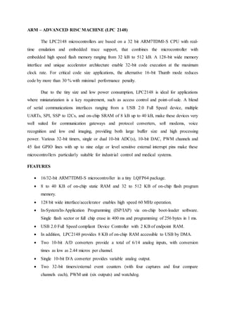
  • 1. ARM – ADVANCED RISC MACHINE (LPC 2148) The LPC2148 microcontrollers are based on a 32 bit ARM7TDMI-S CPU with real- time emulation and embedded trace support, that combines the microcontroller with embedded high speed flash memory ranging from 32 kB to 512 kB. A 128-bit wide memory interface and unique accelerator architecture enable 32-bit code execution at the maximum clock rate. For critical code size applications, the alternative 16-bit Thumb mode reduces code by more than 30 % with minimal performance penalty. Due to the tiny size and low power consumption, LPC2148 is ideal for applications where miniaturization is a key requirement, such as access control and point-of-sale. A blend of serial communications interfaces ranging from a USB 2.0 Full Speed device, multiple UARTs, SPI, SSP to I2Cs, and on-chip SRAM of 8 kB up to 40 kB, make these devices very well suited for communication gateways and protocol converters, soft modems, voice recognition and low end imaging, providing both large buffer size and high processing power. Various 32-bit timers, single or dual 10-bit ADC(s), 10-bit DAC, PWM channels and 45 fast GPIO lines with up to nine edge or level sensitive external interrupt pins make these microcontrollers particularly suitable for industrial control and medical systems. FEATURES  16/32-bit ARM7TDMI-S microcontroller in a tiny LQFP64 package.  8 to 40 KB of on-chip static RAM and 32 to 512 KB of on-chip flash program memory.  128 bit wide interface/accelerator enables high speed 60 MHz operation.  In-System/In-Application Programming (ISP/IAP) via on-chip boot-loader software. Single flash sector or full chip erase in 400 ms and programming of 256 bytes in 1 ms.  USB 2.0 Full Speed compliant Device Controller with 2 KB of endpoint RAM.  In addition, LPC2148 provides 8 KB of on-chip RAM accessible to USB by DMA.  Two 10-bit A/D converters provide a total of 6/14 analog inputs, with conversion times as low as 2.44 micros per channel.  Single 10-bit D/A converter provides variable analog output.  Two 32-bit timers/external event counters (with four captures and four compare channels each), PWM unit (six outputs) and watchdog.
  • 2.  Low power real-time clock with independent power and dedicated 32 kHz clock input.  Multiple serial interfaces including two UARTs (16C550), two Fast I2C-buses  (400 Kbit/s), SPI and SSP with buffering and variable data length capabilities.  Vectored interrupt controller with configurable priorities and vector addresses.  Up to 45 of 5 V tolerant fast general purpose I/O pins in a tiny LQFP64 package.  Up to nine edge or level sensitive external interrupt pins available. 4.1.1 ARCHITECTURAL OVERVIEW The LPC2148 consists of an ARM7TDMI-S CPU with emulation support, the ARM7 Local Bus for interface to on-chip memory controllers, the AMBA Advanced High- performance Bus (AHB) for interface to the interrupt controller, and the ARM Peripheral Bus (APB, a compatible superset of ARM’s AMBA Advanced Peripheral Bus) for connection to on-chip peripheral functions. The LPC2148 configures the ARM7TDMI-S processor in little- endian byte order. AHB peripherals are allocated a 2 megabyte range of addresses at the very top of the 4 gigabyte ARM memory space. Each AHB peripheral is allocated a 16 kB address space within the AHB address space. LPC2148 peripheral functions (other than the interrupt controller) are connected to the APB bus. The AHB to APB bridge interfaces the APB bus to the AHB bus. APB peripherals are also allocated a 2 megabyte range of addresses, beginning at the 3.5 gigabyte address point. Each APB peripheral is allocated a 16 kB address space within the APB address space. The connection of on-chip peripherals to device pins is controlled by a Pin Connect Block. This must be configured by software to fit specific application requirements for the use of peripheral functions and pins.
  • 3. FIG 4.1- Block Diagram of LPC 2148 4.1.2 ARM7TDMI-S PROCESSOR The ARM7TDMI-S is a general purpose 32-bit microprocessor, which offers high performance and very low power consumption. The ARM architecture is based on Reduced Instruction Set Computer (RISC) principles, and the instruction set and related decode mechanism are much simpler than those of micro programmed Complex Instruction Set Computers. This simplicity results in a high instruction throughput and impressive real-time interrupt response from a small and cost-effective processor core. Pipeline techniques are employed so that all parts of the processing and memory systems can operate continuously. Typically, while one instruction is being executed, its successor is being decoded, and a third instruction is being fetched from memory. The ARM7TDMI-S processor also employs a unique architectural strategy known as THUMB, which makes it ideally suited to high- volume applications with memory restrictions or applications where code density is an issue.
  • 4. The key idea behind THUMB is that of a super-reduced instruction set. Essentially, the ARM7TDMI-S processor has two instruction sets: • The standard 32-bit ARM instruction set. • A 16-bit THUMB instruction set. The THUMB set’s 16-bit instruction length allows it to approach twice the density of standard ARM code while retaining most of the ARM’s performance advantage over a traditional 16-bit processor using 16-bit registers. This is possible because THUMB code operates on the same 32-bit register set as ARM code. THUMB code is able to provide up to 65% of the code size of ARM, and 160% of the performance of an equivalent ARM processor connected to a 16-bit memory system. 4.1.3 Description about the Block Diagram: On chip Flash Program Memory LPC 2148 is having 512 k B Flash memory. This memory may be used for both code and data storage. Programming of the flash memory may be accomplished in several ways (ISP/IAP). On chip Static RAM On-chip static RAM may be used for code and/or data storage. The SRAM may be accessed as 8-bit, 16-bit, and 32-bit. An 8 k B SRAM block intended to be utilized mainly by the USB Interrupt Controller The Vectored Interrupt Controller (VIC) accepts all of the interrupt request inputs and categorizes them as Fast Interrupt Request (FIQ), vectored Interrupt Request (IRQ), and non- vectored IRQ as defined by programmable settings. Analog to Digital Converter LPC2148 contains two analog to digital converters (ADC0 & ADC1). Total number of available ADC inputs is 14. These two ADC’s are 10 bit successive approximation analog to digital converters. The measurement range is 0 V to VREF and is Global Start command for both converters.
  • 5. Digital to Analog Converter The DAC enables to generate a variable analog output. The maximum DAC output voltage is the VREF voltage. 10-bit DAC, Buffered output and Power-down mode are available. USB 2.0 Device Controller The USB is a 4-wire serial bus that supports communication between a host and a number (127max) of peripherals. This enables 12 M bit/s data exchange with a USB host controller. A DMA controller (available only in LPC2146/48) can transfer data between an endpoint buffer and the USB RAM. UART LPC2148 contains two UARTs (UART0 & UART1). In addition to standard transmit and receive data lines, the LPC2148 UART1 also provide a full modem control handshake interface. 16 byte Receive and Transmit FIFOs are used. It contains Built-in fractional baud rate generator covering wide range of baud rates without a need for external crystals of particular values. I2C-bus serial I/O controller I2C is a bidirectional. It is a multi-master bus; it can be controlled by more than one bus master connected to it. It supports bit rates up to 400 k bit/s. Bidirectional data transfer between masters and slaves. Serial clock synchronization allows devices with different bit rates to communicate via one serial bus. Serial clock synchronization can be used as a handshake mechanism to suspend and resume serial transfer. SPI serial I/O control It is s a full duplex serial interface, designed to handle multiple masters and slaves connected to a given bus. Synchronous, Serial, Full Duplex Communication is considered in the system. SSP serial I/O control:- Supports full duplex transfers. Data frames of 4 bits to 16 bits of data flowing from the master to the slave and from the slave to the master. Synchronous serial communication
  • 6. Master or slave operation. 8-frame FIFOs for both transmit and receive. Four bits to 16 bits per frame Timers LPC 2148 has two 32-bit timer/counters with a programmable 32-bit pre scalar. It also having external event counter. Four 32-bit capture channels per timer/counter that can take a snapshot of the timer value when an input signals transitions. A capture event may also optionally generate an interrupt.. Watchdog Timer The purpose of the watchdog is to reset the microcontroller within a reasonable amount of time if it enters an erroneous state. When enabled, the watchdog will generate a system reset if the user program fails to ‘feed’ (or reload) the watchdog within a predetermined amount of time. Real Time Clock The RTC is designed to provide a set of counters to measure time when normal or idle Operating mode is selected. The RTC has been designed to use little power, making it Suitable for battery powered systems where the CPU is not running continuously (Idle Mode). Crystal Oscillator On-chip integrated oscillator operates with external crystal in range of 1 MHz to 25 M Hz. The oscillator output frequency is called foscand the ARM processor clock frequency is referred to as CCLK for purposes of rate equations, etc. fosc and CCLK are the same value unless the PLL is running and connected. PLL The PLL accepts an input clock frequency in the range of 10 MHz to 25 MHz’s The input frequency is multiplied up into the range of 10 MHz to 60 MHz with a Current Controlled Oscillator (CCO). The multiplier can be an integer value from 1 to 32 (in practice, the multiplier value cannot be higher than 6 on this family of microcontrollers due to the upper frequency limit of the CPU). The CCO operates in the range of 156 MHz to 320 MHz,
  • 7. so there is an additional divider in the loop to keep the CCO within its frequency range while the PLL is providing the desired output frequency. 4.1.4 LPC 2148 REGISTERS The ARM CPU provides in user mode 16 general purpose registers (R0 - R15) and a Program Status Register. Registers in LPC 2148 are 8, 16 or 32 bits wide. The ARM CPU provides shadow registers which are selected on an Operation Mode switch. These shadow registers reduce interrupt latency. All CPU Registers are shown in the following picture. SP: Stack pointer LR: Link register PC: Program counter CPSR: Current Program Status Register. SPSR: Saved Program Status Register. Fig 4.2: Registers LR (Link register): Used by the processor when there is a branch operation this occurs due to function call or due to some condition checking. When the processor is executing and there is a need to branch to other location the return address (the address from where the execution
  • 8. is to be started, returning after completing the function execution). If there are multiple function calls then LR will store only the last address before jumping. CPSR: Used to store the important back-up data whenever there is change of any mode. E.g. if the processor is executing user mode and there is an interrupt, before going to service the interrupt the all the data and the status registers and the current mode of operation information is stored in CPSR. CPSR registers are present in all the 7 modes but are not usually shown. SPSR: stores the copy of CPSR register in which ever mode the processor enters. All the 7 modes have SPSR registers and are shown in the mode registers. If the processor switches from USER mode to IRQ mode because of an IRQ, the CPSR value is updated in the user mode and the processor switches to IRQ mode. Beforestarting the IRQ code execution the value of CPSR is copied to SPSR of IRQ mode. While executing IRQ mode and high priority interrupt occurs (FIQ) then the status of the IRQ mode is updated in its CPSR register and when the processor switches to FIQ mode the contents of CPSR in IRQ mode is copied to SPSR register in FIQ mode. 4.1.5 General Purpose Input/output ports (GPIO) Every physical GPIO port is accessible either the group of registers by providing an enhanced features and accelerated port access or the legacy group of registers. • Accelerated GPIO functions: – GPIO registers are relocated to the ARM local bus so that the fastest possible I/O Timing can be achieved. – Mask registers allow treating sets of port bits as a group, leaving other bits Unchanged. – All registers are byte and half-word addressable. – Entire port value can be written in one instruction. • Bit-level set and clear registers allow a single instruction set or clear of any number of bits in one port. • Direction control of individual bits. • All I/O default to inputs after reset.
  • 9. • Backward compatibility with other earlier devices is maintained with legacy registers appearing at the original addresses on the VPB bus. Applications: • General purpose I/O • Driving LEDs, or other indicators • Controlling off-chip devices • Sensing digital inputs 4.1.6 Pin Description IOPIN: The current state of the GPIO configured port pins can always be read from this register, regardless of pin direction. IOSET: This register controls the state of output pins in conjunction with the IOCLR register. Writing one’s produces highs at the corresponding port pins. Writing zeroes has no effect. IODIR: GPIO Port Direction control register: This register individually controls the direction of each port pin. Direction bit for any pin must be set according to the pin functionality. IOCLR: GPIO Port Output Clear register: This register controls the state of output pins. Writing ones produces lows at the corresponding port pins and clears the corresponding bits in the IOSET register. Writing zeros has no effect. 4.1.7 PIN diagram of LPC 2148
  • 10. Fig 4.3:Pin diagram of LPC 2148 EXTERNAL INTERRUPT INPUTS The LPC 2148 includes four External Interrupt Inputs as selectable pin functions. The External Interrupt Inputs can optionally be used to wake up the processor from the Power Down mode. REGISTER DESCRIPTION The external interrupt function has four registers associated with it. The EXTINT register contains the interrupt flags, and the EXTWAKEUP register contains bits that enable individual external interrupts to wake up the LPC 2148 from Power Down mode. The EXTMODE and EXTPOLAR registers specify the level and edge sensitivity parameters. External Interrupt Flag Register When a pin is selected for its external interrupt function, the level or edge on that pin selected by its bits in the EXTPOLAR and EXTMODE registers will set its interrupt flag in this register. This asserts the corresponding interrupt request to the VIC, which will cause an interrupt if interrupts from the pin are enabled. Writing ones to bits EINT0 through EINT3 in
  • 11. EXTINT register clears the corresponding bits. In level-sensitive mode this action is efficacious only when the pin is in its inactive state. 4.1.8 UART0 FEATURES • 16 byte Receive and Transmit FIFO. • Register locations conform to ‘550 industry standard. • Receiver FIFO triggers points at 1, 4, 8, and 14 bytes. • Built-in baud rate generator. UART PIN DESCRIPTION Table 4.1: UART PIN description There are two Universal Asynchronous Receiver Transmitters (UART) configured in ARM 7-LPC 2148 viz. UART-0 and UART -1.Register which are related for UART configurations are UO/1LCR, UO/1THR, UO/1RBR and UO/1LSR. LCR: Line Control Register. THR: Transmit Holding Register. RBR: Receive Buffer Register. LSR: Line Status Register. UO/1LSR –
  • 12. 7 6 5 4 3 2 1 0 Divisor latch bit UART trans enb/disable Odd/even parity Enable /disable Parity Bit Stop Bit Width of data Recvd& trans. Bits 1:0- ‘0 0 ‘- 5 bit data. ‘0 1- 6 bit data. ‘1 0 -7 bit data. ‘1 1’- 8 bit data. Bit 2: ‘0’ - 1 stop bit. ‘1’ - 2 stop bits. Bit 3: ‘0’ - Disable parity bit. ‘1’ - Enable parity bit. Bits 4:5 : ‘0 0’ - odd parity. ‘0 1’ – even parity. Bit 6: ‘0’ - Enable transmission bit. ‘1’ - Disable transmission bit. Bit- 7: ‘1’ - to set baud rate. To set baud rate two registers UO/1DLL (Divisor Latch LSB) and U0/1DLM (Divisor Latch MSB) are used.
  • 13. Baud rate value = Processor clock frequency 16* Baud rate (in bits per sec) U0/1LSR: (status of UART) 7 6 5 4 3 2 1 0 X X TRANS STATUS X X X X RECEIV STATUS U0/1THR: Data that is transmitted will be available in U0/1THR and then sent to other registers. U0/1RBR: Data that is received will be available in U0/1THR and then sent to other registers.