Analysis of MOS Capacitor Loaded Annular Ring MICROSTRIP Antenna
•
1 gostou•425 visualizações

In this paper a new technique is proposed for achieving increased frequency agility by loading the patch antenna with a MOS capacitor. Theoretical investigations have been carried out for the MOS capacitor loaded Annular Ring microstrip antenna, for oxide thicknesses from 100 A to 500 A, to predict the achievable range of operational bandwidth. In spite of numerous advantages, the simple patch antenna has a low operational bandwidth, which limits its applicability. Hence this technique of MOS capacitor loaded Annular Ring microstrip patch antenna is to improve the operating frequency range.

Recomendados
Recomendados
Mais conteúdo relacionado
Mais procurados
Mais procurados (19)
Destaque
Destaque (20)
Semelhante a Analysis of MOS Capacitor Loaded Annular Ring MICROSTRIP Antenna
Semelhante a Analysis of MOS Capacitor Loaded Annular Ring MICROSTRIP Antenna (20)
Mais de IJMER
Mais de IJMER (20)
Último
Último (20)
Analysis of MOS Capacitor Loaded Annular Ring MICROSTRIP Antenna
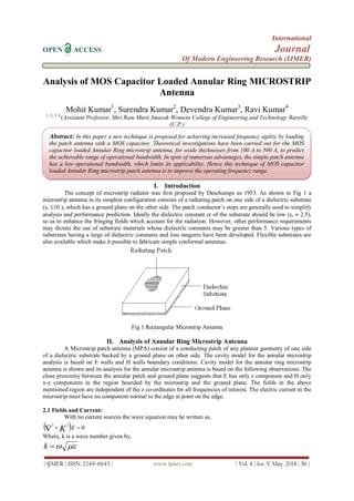
- 1. International OPEN ACCESS Journal Of Modern Engineering Research (IJMER) | IJMER | ISSN: 2249–6645 | www.ijmer.com | Vol. 4 | Iss. 5| May. 2014 | 56 | Analysis of MOS Capacitor Loaded Annular Ring MICROSTRIP Antenna Mohit Kumar1 , Surendra Kumar2 , Devendra Kumar3 , Ravi Kumar4 1, 2, 3, 4 (Assistant Professor, Shri Ram Murti Smarak Womens College of Engineering and Technology Bareilly (U.P.) I. Introduction The concept of microstrip radiator was first proposed by Deschamps as 1953. As shown in Fig 1 a microstrip antenna in its simplest configuration consists of a radiating patch on one side of a dielectric substrate (r 10 ), which has a ground plane on the other side. The patch conductor’s steps are generally used to simplify analysis and performance prediction. Ideally the dielectric constant r of the substrate should be low (r 2.5), so as to enhance the fringing fields which account for the radiation. However, other performance requirements may dictate the use of substrate materials whose dielectric constants may be greater than 5. Various types of substrates having a large of dielectric constants and loss tangents have been developed. Flexible substrates are also available which make it possible to fabricate simple conformal antennas. Fig 1 Rectangular Microstrip Antenna II. Analysis of Annular Ring Microstrip Antenna A Microstrip patch antenna (MPA) consist of a conducting patch of any planner geometry of one side of a dielectric substrate backed by a ground plane on other side. The cavity model for the annular microstrip analysis is based on E walls and H walls boundary conditions. Cavity model for the annular ring microstrip antenna is shown and its analysis for the annular microstrip antenna is based on the following observations. The close proximity between the annular patch and ground plane suggests that E has only z component and H only x-y components in the region bounded by the microstrip and the ground plane. The fields in the above mentioned region are independent of the z co-ordinates for all frequencies of interest. The electric current in the microstrip must have no component normal to the edge at point on the edge. 2.1 Fields and Current: With no current sources the wave equation may be written as, 0 22 EK Where, k is a wave number given by, k Abstract: In this paper a new technique is proposed for achieving increased frequency agility by loading the patch antenna with a MOS capacitor. Theoretical investigations have been carried out for the MOS capacitor loaded Annular Ring microstrip antenna, for oxide thicknesses from 100 A to 500 A, to predict the achievable range of operational bandwidth. In spite of numerous advantages, the simple patch antenna has a low operational bandwidth, which limits its applicability. Hence this technique of MOS capacitor loaded Annular Ring microstrip patch antenna is to improve the operating frequency range.
- 2. Analysis of MOS Capacitor Loaded Annular Ring Microstrip Antenna | IJMER | ISSN: 2249–6645 | www.ijmer.com | Vol. 4 | Iss. 5| May. 2014 | 57 | The field must be solved by the wave equation and the magnetic wall boundary conditions. Since, EZE z , 0| a E and 0| b E Thus the solution of the wave equation in the cylindrical; co-ordinates is 0 cos)()()()( // 0 EE YjYjEE nkkkak nnnnz 2.2 Resonant Frequency: The resonant frequency can be calculated by taking account the effect of fringing field rknmcf nm 2/ Here c is the velocity of light and r the relative dielectric constant 2.3 Effective Inner and Outer Radii & Effective Dielectric Constant: To account the fringing field effects along the curved edges of the ring it is necessary to replace the radius ‘a’ and ‘b’ by their effective values, aeff, beff and eff can be calculate as follows )( 10 1 2/1 )1( 2 1 )1( 2 1 w h rreff Now the resonant wave number knm is the m zero of the transcendental equation 0)()()()( //// kaYkbjkbYkaj nmennmennmennmen for the TM12 mode the solution of the above equation is given by ))(( 8.17 975.51 12 baab a k eeee e After solving the characteristic equation for knm, the resonant frequency can be determined from eff nm nm kf c 2 It should be pointed out that the correction to the resonant frequency formula involves both the effective permittivity and the effective radii. 2.4 Input Impedance: Equivalent circuit is effective to design for this type of antenna because of its simplicity and ease of understanding the physical phenomenon. It is a G-L-G lumped element resonator circuit. Using the mode expansion theory, the input impedance of the AR-MSA can be obtained. The input impedance from the feed line can be expressed as a parallel resonator, L G L c Z t n m nm nm nm in j jj 1 1 Where Cnm, Lnm, and Gnm are equivalent circuit parameters including losses corresponding to each mode. III. Analysis of Annular Micro strip Antenna with MOS Capacitor Loaded 3.1 Mos Capacitor: A MOS capacitor of MIS (metal± insulator± semiconductor) diode is a voltage variable capacitor. A typical MOS capacitor structure for the proposed analysis is Au± Si3N4± Si, shown in The capacitance is dependent on the oxide thickness, which is evidently clear from d a C . Mos capacitance
- 3. Analysis of MOS Capacitor Loaded Annular Ring Microstrip Antenna | IJMER | ISSN: 2249–6645 | www.ijmer.com | Vol. 4 | Iss. 5| May. 2014 | 58 | A qNa VgC C Cmos 212 0 0 2 1 The capacitance of the depletion Cd per unit area qNa VgCC C . 2 1 1 2 00 The ratio of C/Co decreases with the gate potential accordance with the above expression, and reaches a minimum value when inversion layer is formed. 3.2 Mos Capacitor Loaded Annular Ring Microstrip Antenna Equivalent circuit for MOS loaded annular ring microstrip antenna is shown below Fig 2 Equivalent circuit for MOS Loaded annular ring microstrip antenna The patch performance will be affected due to its radiating edge capacitance in addition to the capacitance provided due to the MOS capacitor Under such conditions the total capacitance will be CCCCC EQSBSAMOStotal Where )65.1268.0()77.141.1( 2 ln2 2 0 rrSA ah a a t C )65.1268.0()77.141.1( 2 ln2 2 0 rrSB bh b b t C Thus the resonance frequency for the modified mode will be )( 2/1 2 1 CL f totalEQ r IV. Computation of Various Parameters 4.1 Reflection coefficient: It is defined as the ratio of the reflected voltage or current to the incident voltage or current and is usually denoted by ρ. Reflection coefficient is a vector quantity having magnitude and direction as well. In terms of impedance it can be expressed as ZZ ZZ in in 0 0 4.2 Voltage standing wave ratio: It is defined as ratio of maximum to minimum voltage on a line having standing waves and this ratio is observed as VSWR= 1 1 4.3 Input impedance of the patch: When we consider only the annular ring patch, than the input impedance will be Zin R+iX
- 4. Analysis of MOS Capacitor Loaded Annular Ring Microstrip Antenna | IJMER | ISSN: 2249–6645 | www.ijmer.com | Vol. 4 | Iss. 5| May. 2014 | 59 | 4.4 Quality factor: It is a measure of any selectivity of a resonant or anti resonant current and is expressed as Q=ωW/P W=Maximum stored energy P=average power loss Fig 3 Input Impedance vs Frequency for different feed points Fig 4 VSWR vs Frequency Fig 5 Return Loss vs Frequency Voltage Fig 6 MOS Capacitance vs Bias Fig 7 Resonating Frequency vs Bias Voltage Fig 8 Input Impedance vs Frequency for MOS Loaded ARMSA V. Conclusion This paper has described an analysis of the behavior of Mos capacitor loaded annular ring microstrip antenna. Results have been presented for resonant frequencies and radiation patterns. After loading MOS capacitor on the antenna the operating frequency can be easily controlled. From above graphical analysis it is observed that- 1. The variation of MOS capacitance is similar for all the five oxide thickness. A larger variation in capacitance is observed with bias voltage near zero bias, but it is very small at higher bias. 2. The maximum frequency agility of 57.08% is obtained for minimum oxide thickness (100A˚ ). However for maximum value of oxide thickness (500 A˚), the frequency agility is around 38.48% (0.962 GHz),
- 5. Analysis of MOS Capacitor Loaded Annular Ring Microstrip Antenna | IJMER | ISSN: 2249–6645 | www.ijmer.com | Vol. 4 | Iss. 5| May. 2014 | 60 | which is the lowest value. The frequency agility obtained with the MOS capacitor loaded antenna (57.08 % ) is higher than the varactor loaded patch ( 47.24 % ). REFRENCES [1] I .J. Bhal and P. Bhartia , Microstrip Antenna , Dedham , MA : Arteh House , 1980 , [2] Special issue on microstrip antennas, IEEE Trans. Antennas Propagation , vol . AP- 29, Jan. 1981. [3] I. J. Bhal , S . S . Stuchly , and M . A .Stuchly , “A new microstrip radiator for medival application , “ IEEE Trans Microwave Theory Tech., vol. MTT-28, pp. 1464-1468, 1980. [4] J. W. Mink, “Circular ring microstrip antenna elements, “presented at 1980 Antennas Propagat . Soc. Int. Symp. , P.Q, Canada , June 1980. [5] S. Ali, W. C. Chew, and J. A. Kong, “Vector Hankel transform analysis of annular ring microstrip antenna , “IEEE Trans . Antenna Propagat . , vol . AP-30 [6] W.C. Chew, “A broad – band annular – ring microstrip antenna , “ IEEE Trans. Antennas Propagation , vol . AP- 30, no. 5, pp. 918-922 , Sept. 1982. [7] J. S. Dahele and K. D. Lee, “Characteristics of annular ring microstrip antenna, “Electron . Lett. , vol . 18, pp . 1051-1053, Nov.1982. [8] L. C. Shen , “analysis of a circular disc printed circuit antenna , “ Proc. Inst . Elec, Eng., vol , 126,no.12 pp.1220-1222, Dec. 1979.