SlideShare uma empresa Scribd logo
1 de 4
Baixar para ler offline
TERM PAPER OF ECE-563, NOVEMBER, 2014
BICMOS
Himanshu Shekhar
ABSTRACT
This paper deals with BICMOS. First of all
the need of transistor is justified. After this it
is explained, the reason behind switching
from vacuum tube to BJT to FET to
BICMOS. Then simple working of BICMOS
inverter working, its advantages,
disadvantages and its application.
I. INTRODUCTION
The transistor is a three terminal, solid state
electronic device. In a three terminal device
we can control electric current or voltage
between two of the terminals by applying an
electric current or voltage to the third
terminal. This three terminal character of the
transistor is what allows us to make an
amplifier for electrical signals, like the one in
our radio. With the three-terminal transistor
we can also make an electric switch, which
can be controlled by another electrical
switch. Before transistor vacuum tube were
the device that were used for control
conduction. But Vacuum tube had to warm
up before they worked (and sometimes
overheated when they did), they were
unreliable and bulky and they used too much
energy.so we moved toward BJT, to reduce
power consumption, area and increase
execution speed and more reliable. But for
low power application and to reduce leakage
current in BJT, FET was developed and most
famous one is CMOS. From early 1980s BJT
and CMOS are combined together to make a
transistor that uses plus point of both to
nullify the negative points of both.
II. BICMOS
BICMOS is a combination of both bipolar
and CMOS that allows the designer to use
both devices on a single integrated circuit.
The development of BICMOS technology
began in the early 1980s. In general, bipolar
devices are attractive because of their high
speed, better gain, better driving capability,
and low wideband noise properties that allow
high-quality analog performance. CMOS is
particularly attractive for digital applications
because of its low power and high packing
density. Thus, the combination of both device
types would not only lead to the replacement
and improvement of existing integrated
circuit, but would also provide access to
design completely new circuits.
Let’s take an example to know the
importance of BICMOS.
Fig.1 Cascade inverter
As shown in Fig. 1 cascaded inverter is made
to drive a bigger load than just a single
inverter, and this has to do with speed. The
problem is that a CMOS gate can drive a
current proportionally to the width of its
channel: so doubling the channel width, we
will be able to charge a capacitor twice as
fast.
If we double the channel width, it also
double the input capacitance of the gate, so
the stage before will take twice the time to
drive the gate. So we need a gate which has
the minimum possible input capacitance,
while having as much as driving strength as
possible. This is obtained cascading several
inverters (the most elementary CMOS gate)
with increasing channel width, so that the
first has the required input capacitance and
the last has the required driving strength. In
comparison, bipolar junction transistors
(BJTs) have more current driving capability,
and hence, can overcome such speed
bottlenecks using less silicon area. However,
the power dissipation of bipolar logic gates is
typically one or two orders of magnitude
larger than that of comparable CMOS gates.
Therefore, such all-bipolar high speed VLSI
circuit are difficult to realize and require very
elaborate heat-sink arrangements.
An alternative solution to the problem of
driving large capacitive loads can be provide
by merging CMOS and bipolar devices
(BICMOS) on chip Taking advantage of the
low static power consumption of CMOS and
the high current driving capability of the
bipolar transistor during transients, the
BICMOS configuration
The BICMOS combination has significant
advantages to offer, such as improved
switching speed and less sensitivity with
respect to the load capacitance. BICMOS
logic circuits are not bipolar-intensive i.e.
most logic operations are performed by
conventional CMOS sub circuits, while the
bipolar transistors are used only when high
on-chip or off-chip drive capability is
required.
III. BASIC BICMOS CIRCUIT
In BICMOS inverter as shown in Fig. 2, the
complementary pMOS and nMOS transistors
MP and MN supply base currents to the
bipolar transistor and thus act as a trigger
device for bipolar output stage configuration.
Depending on the logic level of the input
voltage, either MN or MP can be turned on in
steady state, therefore assuring a fully
complementary push pull operation mode for
the two bipolar transistors. In this very
simplistic configuration, configuration, two
resistors are used to remove the base charge
of the bipolar transistors when they are when
they are in cut-off mode
Fig. 2 Simple BICMOS inverter circuit with
resistive base pull-down.
The superiority of the BICMOS gate lies in
the high current drive capability of the
bipolar output transistors, the zero static
power dissipation, and the high input
impedance provided by the MOSFET
configuration. To reduce the turn-off time of
the bipolar transistors during switching,
Two minimum-size nMOS transistors (MB1
and MB2) are usually added to provide the
necessary base Discharge path, instead of the
two resistors. As shown in Fig.3
Fig. 3 Conventional BICMOS inverter
circuit with active base pull-down
V. BICMOS INVERTER
Consider first the output pull-up transient
response, which starts with the input voltage
abruptly falling from VOH to VOL at t = 0.
The initial condition of the output node
voltage is assumed to be VO, = VOH. The
inverter circuit during this switching event is
depicted in Fig.4, where the active
(conducting) devices are highlighted.
Fig. 4: BiCMOS inverter during transient
output pull-up event. The active devices in
thecircuit are highlighted (darker).
As the input voltage drops, the pMOS
transistor MP is turned on and starts
operating in the saturation region. The nMOS
transistors MN and MB 1 are turned off; thus,
the lower "pull-down" part of the inverter
circuit can be ignored except for the
corresponding parasitic capacitances of the
nMOS transistors and the bipolar transistor
Q2. The base pull-down transistor MB2 is
turned on, which effectively drains the excess
base minority carrier charge of Q2 and
assures that Q2 remains in cut-off mode. At
the same time, MP is supplying the base
current of Q1, which starts to charge up Cload
with its emitter current.
Now consider the output pull-down transient
response, which starts with the input voltage
abruptly rising from VOL to VOH at t = 0.
The initial condition of the output node
voltage is assumed to be Vout = VOL. The
inverter circuit during this switching event is
depicted in Fig.5, where the active
(conducting) devices are highlighted.
Fig. 5: BiCMOS inverter during a transient
output pull-down event.The active devices in
the circuit are highlighted (darker).
As the input voltage rises, the pMOS
transistor MP is turned off and the nMOS
Transistors MN and MB 1 are turned on. The
bipolar pull-up transistor Q1 immediately
ceases to conduct because its base current
drops to zero, and MB 1 starts to remove the
excess minority carrier base charge of Q1.
The nMOS transistor MN operates initially in
the saturation region and supplies the base
current of the bipolar pull-down transistor
Q2.
IV. USES OF BICMOS TECHNOLOGY
There have been two significant uses of
BICMOS technology.
One of the usages is in the design of the high-
performance microprocessor unit (MPU)
using the high driving capability of bipolar
junction transistor because bipolar junction
transistor has better transconductance.
Comparing the gate delay time and load
capacitance capability for same area design,
BICMOS has a lower gate delay time than the
CMOS at high load capacitive environment
as illustrated in Fig 6.
Fig. 6 CMOS vs BICMOS
And second one is in the mixed signal circuit
design, BICMOS design utilizes the excellent
analog performance of the double poly self-
aligned bipolar junction transistor
V. BICMOS APPLICATION
1. In some applications (in which there is
finite budget for power) the BICMOS speed
performance is better than that of bipolar.
2. This technology is well suited for the
intensive input/output applications.
3. The applications of BICMOS were initially
in RISC microprocessors rather than
traditional CISC microprocessors.
4. It can be used for sample and hold
applications as it provides high impedance
inputs.
5. This is also used in applications such as
adders, mixers, ADC and DAC
VI. CONCLUSION
The most significant drawback of the
BICMOS circuits lies in the increased
fabrication process complexity more than
that of CMOS. Apart from this it can be used
as an alternate of the previous bipolar, ECL
and CMOS in the market.
VII. REFERENCE
[1] http://www.nobelprize.org
[2] http://blog.oscarliang.net/bjt-vs-mosfet
[3] http:// www.elprocus.com
[4] Digital Integrated Circuits, 2/E Jan M.
Rabaey, University of California, Berkeley
Anantha Chandrakasan, Massachusetts
Institute of Technology, Cambridge Borivoje
Nikolic, University of California, Berkeley.
[5] CMOS Digital integrated Circuits Sung-
Mo-Kang & Yusuf Leblebici 3rd 2003 Tata
McGraw Hill

Mais conteúdo relacionado

Mais procurados

Supervisor call and pendable service call
Supervisor call and pendable service callSupervisor call and pendable service call
Supervisor call and pendable service callPriyangaKR1
 
Introduction to VLSI Technology
Introduction to VLSI TechnologyIntroduction to VLSI Technology
Introduction to VLSI TechnologyDr.YNM
 
Ph.d. thesis modeling and simulation of z source inverter design and its con...
Ph.d. thesis  modeling and simulation of z source inverter design and its con...Ph.d. thesis  modeling and simulation of z source inverter design and its con...
Ph.d. thesis modeling and simulation of z source inverter design and its con...Dr. Pankaj Zope
 
Tunnel field effect transistor
Tunnel field effect transistorTunnel field effect transistor
Tunnel field effect transistor祖文 宋
 
Advances in VLSI Chapter 6 Superbuffers
Advances in VLSI Chapter 6 SuperbuffersAdvances in VLSI Chapter 6 Superbuffers
Advances in VLSI Chapter 6 SuperbuffersDabbaru Murali
 
Single Ended Schmitt Trigger Based Robust Low Power SRAM Cell
Single Ended Schmitt Trigger Based Robust Low Power SRAM CellSingle Ended Schmitt Trigger Based Robust Low Power SRAM Cell
Single Ended Schmitt Trigger Based Robust Low Power SRAM CellVishwanath Hiremath
 
Introduction to pll
Introduction to pllIntroduction to pll
Introduction to pllsartaj ahmed
 
MOS and BiCMOS Circuit design Process
MOS and BiCMOS Circuit design ProcessMOS and BiCMOS Circuit design Process
MOS and BiCMOS Circuit design ProcessDr.YNM
 
Review on Tunnel Field Effect Transistors (TFET)
Review on Tunnel Field Effect Transistors (TFET)Review on Tunnel Field Effect Transistors (TFET)
Review on Tunnel Field Effect Transistors (TFET)IRJET Journal
 
An Automatic Generation of NoC Architectures: An Application-Mapping Approach
An Automatic Generation of NoC Architectures: An Application-Mapping ApproachAn Automatic Generation of NoC Architectures: An Application-Mapping Approach
An Automatic Generation of NoC Architectures: An Application-Mapping ApproachMostafa Khamis
 
SEMICONDUCTOR MEMORIES(RAM &ROM).pptx
SEMICONDUCTOR MEMORIES(RAM &ROM).pptxSEMICONDUCTOR MEMORIES(RAM &ROM).pptx
SEMICONDUCTOR MEMORIES(RAM &ROM).pptxMomin24
 
Bicmos Technology - Overview
Bicmos Technology - OverviewBicmos Technology - Overview
Bicmos Technology - OverviewAyush Mittal
 
Generate pwm signal through arduino of various duty
Generate pwm signal through arduino of various dutyGenerate pwm signal through arduino of various duty
Generate pwm signal through arduino of various dutyPANKAJPRAJAPATI45
 

Mais procurados (20)

Supervisor call and pendable service call
Supervisor call and pendable service callSupervisor call and pendable service call
Supervisor call and pendable service call
 
Introduction to VLSI Technology
Introduction to VLSI TechnologyIntroduction to VLSI Technology
Introduction to VLSI Technology
 
Microprocessor interview questions
Microprocessor interview questionsMicroprocessor interview questions
Microprocessor interview questions
 
Bicoms
BicomsBicoms
Bicoms
 
Ph.d. thesis modeling and simulation of z source inverter design and its con...
Ph.d. thesis  modeling and simulation of z source inverter design and its con...Ph.d. thesis  modeling and simulation of z source inverter design and its con...
Ph.d. thesis modeling and simulation of z source inverter design and its con...
 
Tunnel field effect transistor
Tunnel field effect transistorTunnel field effect transistor
Tunnel field effect transistor
 
Advances in VLSI Chapter 6 Superbuffers
Advances in VLSI Chapter 6 SuperbuffersAdvances in VLSI Chapter 6 Superbuffers
Advances in VLSI Chapter 6 Superbuffers
 
Single Ended Schmitt Trigger Based Robust Low Power SRAM Cell
Single Ended Schmitt Trigger Based Robust Low Power SRAM CellSingle Ended Schmitt Trigger Based Robust Low Power SRAM Cell
Single Ended Schmitt Trigger Based Robust Low Power SRAM Cell
 
Introduction to pll
Introduction to pllIntroduction to pll
Introduction to pll
 
MOS and BiCMOS Circuit design Process
MOS and BiCMOS Circuit design ProcessMOS and BiCMOS Circuit design Process
MOS and BiCMOS Circuit design Process
 
FPGA Introduction
FPGA IntroductionFPGA Introduction
FPGA Introduction
 
Review on Tunnel Field Effect Transistors (TFET)
Review on Tunnel Field Effect Transistors (TFET)Review on Tunnel Field Effect Transistors (TFET)
Review on Tunnel Field Effect Transistors (TFET)
 
Vlsi ppt priyanka
Vlsi ppt priyankaVlsi ppt priyanka
Vlsi ppt priyanka
 
GUI for DRV fix in ICC2
GUI for DRV fix in ICC2GUI for DRV fix in ICC2
GUI for DRV fix in ICC2
 
An Automatic Generation of NoC Architectures: An Application-Mapping Approach
An Automatic Generation of NoC Architectures: An Application-Mapping ApproachAn Automatic Generation of NoC Architectures: An Application-Mapping Approach
An Automatic Generation of NoC Architectures: An Application-Mapping Approach
 
SEMICONDUCTOR MEMORIES(RAM &ROM).pptx
SEMICONDUCTOR MEMORIES(RAM &ROM).pptxSEMICONDUCTOR MEMORIES(RAM &ROM).pptx
SEMICONDUCTOR MEMORIES(RAM &ROM).pptx
 
Bicmos Technology - Overview
Bicmos Technology - OverviewBicmos Technology - Overview
Bicmos Technology - Overview
 
Clock Distribution
Clock DistributionClock Distribution
Clock Distribution
 
MOSFET Amplifier
MOSFET AmplifierMOSFET Amplifier
MOSFET Amplifier
 
Generate pwm signal through arduino of various duty
Generate pwm signal through arduino of various dutyGenerate pwm signal through arduino of various duty
Generate pwm signal through arduino of various duty
 

Destaque (12)

BiCMOS Technology
BiCMOS TechnologyBiCMOS Technology
BiCMOS Technology
 
72 129-135
72 129-13572 129-135
72 129-135
 
Ee660 ex 24_bi_cmos_comparisons_all
Ee660 ex 24_bi_cmos_comparisons_allEe660 ex 24_bi_cmos_comparisons_all
Ee660 ex 24_bi_cmos_comparisons_all
 
Ijeee 24-27-energy efficient communication for adhoc networks
Ijeee 24-27-energy efficient communication for adhoc networksIjeee 24-27-energy efficient communication for adhoc networks
Ijeee 24-27-energy efficient communication for adhoc networks
 
Ijsws14 458-paper-18-piconet
Ijsws14 458-paper-18-piconetIjsws14 458-paper-18-piconet
Ijsws14 458-paper-18-piconet
 
3D Holographic Projection Technology
3D Holographic Projection Technology3D Holographic Projection Technology
3D Holographic Projection Technology
 
Solar Power Satellites
Solar Power SatellitesSolar Power Satellites
Solar Power Satellites
 
Basics of CT Scan
Basics of CT ScanBasics of CT Scan
Basics of CT Scan
 
Basic principles of CT scanning
Basic principles of CT scanningBasic principles of CT scanning
Basic principles of CT scanning
 
Computer Tomography (CT Scan)
Computer Tomography (CT Scan)Computer Tomography (CT Scan)
Computer Tomography (CT Scan)
 
Ct Basics
Ct BasicsCt Basics
Ct Basics
 
Solar Power Satellite
Solar Power SatelliteSolar Power Satellite
Solar Power Satellite
 

Semelhante a Modified bicmos

Distortion Analysis of Differential Amplifier
Distortion Analysis of Differential AmplifierDistortion Analysis of Differential Amplifier
Distortion Analysis of Differential AmplifierIOSR Journals
 
Introduction to MOS Technology.pdf
Introduction to MOS Technology.pdfIntroduction to MOS Technology.pdf
Introduction to MOS Technology.pdfAshishSoni509
 
Variable Threshold MOSFET Approach (Through Dynamic Threshold MOSFET) For Uni...
Variable Threshold MOSFET Approach (Through Dynamic Threshold MOSFET) For Uni...Variable Threshold MOSFET Approach (Through Dynamic Threshold MOSFET) For Uni...
Variable Threshold MOSFET Approach (Through Dynamic Threshold MOSFET) For Uni...VLSICS Design
 
Design of A Low Power Low Voltage CMOS Opamp
Design of A Low Power Low Voltage CMOS OpampDesign of A Low Power Low Voltage CMOS Opamp
Design of A Low Power Low Voltage CMOS OpampVLSICS Design
 
Design of Low Voltage D-Flip Flop Using MOS Current Mode Logic (MCML) For Hig...
Design of Low Voltage D-Flip Flop Using MOS Current Mode Logic (MCML) For Hig...Design of Low Voltage D-Flip Flop Using MOS Current Mode Logic (MCML) For Hig...
Design of Low Voltage D-Flip Flop Using MOS Current Mode Logic (MCML) For Hig...IOSRJVSP
 
M.TECH IEEE.Technical seminar paper for Vlsi design and embedded systems.
M.TECH IEEE.Technical seminar paper for Vlsi design and embedded systems.M.TECH IEEE.Technical seminar paper for Vlsi design and embedded systems.
M.TECH IEEE.Technical seminar paper for Vlsi design and embedded systems.Suchitra goudar
 
Basic knowledge of ldo voltage regulators
Basic knowledge of ldo voltage regulatorsBasic knowledge of ldo voltage regulators
Basic knowledge of ldo voltage regulatorsĐức Hữu
 
MOSFET, SOI-FET and FIN-FET-ABU SYED KUET
MOSFET, SOI-FET and FIN-FET-ABU SYED KUETMOSFET, SOI-FET and FIN-FET-ABU SYED KUET
MOSFET, SOI-FET and FIN-FET-ABU SYED KUETA. S. M. Jannatul Islam
 
IRJET- Design of 4th Order Low Pass Filter using Memristive OP-AMPS
IRJET- Design of 4th Order Low Pass Filter using Memristive OP-AMPSIRJET- Design of 4th Order Low Pass Filter using Memristive OP-AMPS
IRJET- Design of 4th Order Low Pass Filter using Memristive OP-AMPSIRJET Journal
 
Delay Optimized Full Adder Design for High Speed VLSI Applications
Delay Optimized Full Adder Design for High Speed VLSI ApplicationsDelay Optimized Full Adder Design for High Speed VLSI Applications
Delay Optimized Full Adder Design for High Speed VLSI ApplicationsIRJET Journal
 
Implementation of Full Adder Cell Using High Performance CMOS Technology
Implementation of Full Adder Cell Using High Performance CMOS TechnologyImplementation of Full Adder Cell Using High Performance CMOS Technology
Implementation of Full Adder Cell Using High Performance CMOS Technologyijsrd.com
 
Design of 64 bit SRAM using Lector Technique for Low Leakage Power with Read ...
Design of 64 bit SRAM using Lector Technique for Low Leakage Power with Read ...Design of 64 bit SRAM using Lector Technique for Low Leakage Power with Read ...
Design of 64 bit SRAM using Lector Technique for Low Leakage Power with Read ...IOSRJVSP
 
Pipelining approach
Pipelining approachPipelining approach
Pipelining approachGopinathD17
 

Semelhante a Modified bicmos (20)

bicmos.pdf
bicmos.pdfbicmos.pdf
bicmos.pdf
 
D41022328
D41022328D41022328
D41022328
 
Distortion Analysis of Differential Amplifier
Distortion Analysis of Differential AmplifierDistortion Analysis of Differential Amplifier
Distortion Analysis of Differential Amplifier
 
12BiCMOS Technology.ppt
12BiCMOS Technology.ppt12BiCMOS Technology.ppt
12BiCMOS Technology.ppt
 
Introduction to MOS Technology.pdf
Introduction to MOS Technology.pdfIntroduction to MOS Technology.pdf
Introduction to MOS Technology.pdf
 
Variable Threshold MOSFET Approach (Through Dynamic Threshold MOSFET) For Uni...
Variable Threshold MOSFET Approach (Through Dynamic Threshold MOSFET) For Uni...Variable Threshold MOSFET Approach (Through Dynamic Threshold MOSFET) For Uni...
Variable Threshold MOSFET Approach (Through Dynamic Threshold MOSFET) For Uni...
 
Ijetr011811
Ijetr011811Ijetr011811
Ijetr011811
 
Design of A Low Power Low Voltage CMOS Opamp
Design of A Low Power Low Voltage CMOS OpampDesign of A Low Power Low Voltage CMOS Opamp
Design of A Low Power Low Voltage CMOS Opamp
 
Bf044352356
Bf044352356Bf044352356
Bf044352356
 
Design of Low Voltage D-Flip Flop Using MOS Current Mode Logic (MCML) For Hig...
Design of Low Voltage D-Flip Flop Using MOS Current Mode Logic (MCML) For Hig...Design of Low Voltage D-Flip Flop Using MOS Current Mode Logic (MCML) For Hig...
Design of Low Voltage D-Flip Flop Using MOS Current Mode Logic (MCML) For Hig...
 
M.TECH IEEE.Technical seminar paper for Vlsi design and embedded systems.
M.TECH IEEE.Technical seminar paper for Vlsi design and embedded systems.M.TECH IEEE.Technical seminar paper for Vlsi design and embedded systems.
M.TECH IEEE.Technical seminar paper for Vlsi design and embedded systems.
 
1576330771.pdf
1576330771.pdf1576330771.pdf
1576330771.pdf
 
Basic knowledge of ldo voltage regulators
Basic knowledge of ldo voltage regulatorsBasic knowledge of ldo voltage regulators
Basic knowledge of ldo voltage regulators
 
MOSFET, SOI-FET and FIN-FET-ABU SYED KUET
MOSFET, SOI-FET and FIN-FET-ABU SYED KUETMOSFET, SOI-FET and FIN-FET-ABU SYED KUET
MOSFET, SOI-FET and FIN-FET-ABU SYED KUET
 
IRJET- Design of 4th Order Low Pass Filter using Memristive OP-AMPS
IRJET- Design of 4th Order Low Pass Filter using Memristive OP-AMPSIRJET- Design of 4th Order Low Pass Filter using Memristive OP-AMPS
IRJET- Design of 4th Order Low Pass Filter using Memristive OP-AMPS
 
Delay Optimized Full Adder Design for High Speed VLSI Applications
Delay Optimized Full Adder Design for High Speed VLSI ApplicationsDelay Optimized Full Adder Design for High Speed VLSI Applications
Delay Optimized Full Adder Design for High Speed VLSI Applications
 
Implementation of Full Adder Cell Using High Performance CMOS Technology
Implementation of Full Adder Cell Using High Performance CMOS TechnologyImplementation of Full Adder Cell Using High Performance CMOS Technology
Implementation of Full Adder Cell Using High Performance CMOS Technology
 
Design of 64 bit SRAM using Lector Technique for Low Leakage Power with Read ...
Design of 64 bit SRAM using Lector Technique for Low Leakage Power with Read ...Design of 64 bit SRAM using Lector Technique for Low Leakage Power with Read ...
Design of 64 bit SRAM using Lector Technique for Low Leakage Power with Read ...
 
Pipelining approach
Pipelining approachPipelining approach
Pipelining approach
 
CMOS
CMOS CMOS
CMOS
 

Mais de Himanshu Shekhar

Mais de Himanshu Shekhar (7)

Connecting devices
Connecting devicesConnecting devices
Connecting devices
 
Static variable
Static variableStatic variable
Static variable
 
Sample Resume
Sample Resume Sample Resume
Sample Resume
 
Questionnaire on Mobile usage
Questionnaire on Mobile usageQuestionnaire on Mobile usage
Questionnaire on Mobile usage
 
time hopping spread spectrum term paper
time hopping spread spectrum term papertime hopping spread spectrum term paper
time hopping spread spectrum term paper
 
SWITCH FROM TRADITIONAL TO MODERN CRYPTOGRAPHY
SWITCH FROM TRADITIONAL TO MODERN CRYPTOGRAPHYSWITCH FROM TRADITIONAL TO MODERN CRYPTOGRAPHY
SWITCH FROM TRADITIONAL TO MODERN CRYPTOGRAPHY
 
Quantum cryptography
Quantum cryptographyQuantum cryptography
Quantum cryptography
 

Último

Call for Papers - African Journal of Biological Sciences, E-ISSN: 2663-2187, ...
Call for Papers - African Journal of Biological Sciences, E-ISSN: 2663-2187, ...Call for Papers - African Journal of Biological Sciences, E-ISSN: 2663-2187, ...
Call for Papers - African Journal of Biological Sciences, E-ISSN: 2663-2187, ...Christo Ananth
 
Microscopic Analysis of Ceramic Materials.pptx
Microscopic Analysis of Ceramic Materials.pptxMicroscopic Analysis of Ceramic Materials.pptx
Microscopic Analysis of Ceramic Materials.pptxpurnimasatapathy1234
 
Call Girls in Nagpur Suman Call 7001035870 Meet With Nagpur Escorts
Call Girls in Nagpur Suman Call 7001035870 Meet With Nagpur EscortsCall Girls in Nagpur Suman Call 7001035870 Meet With Nagpur Escorts
Call Girls in Nagpur Suman Call 7001035870 Meet With Nagpur EscortsCall Girls in Nagpur High Profile
 
High Profile Call Girls Nagpur Meera Call 7001035870 Meet With Nagpur Escorts
High Profile Call Girls Nagpur Meera Call 7001035870 Meet With Nagpur EscortsHigh Profile Call Girls Nagpur Meera Call 7001035870 Meet With Nagpur Escorts
High Profile Call Girls Nagpur Meera Call 7001035870 Meet With Nagpur EscortsCall Girls in Nagpur High Profile
 
OSVC_Meta-Data based Simulation Automation to overcome Verification Challenge...
OSVC_Meta-Data based Simulation Automation to overcome Verification Challenge...OSVC_Meta-Data based Simulation Automation to overcome Verification Challenge...
OSVC_Meta-Data based Simulation Automation to overcome Verification Challenge...Soham Mondal
 
AKTU Computer Networks notes --- Unit 3.pdf
AKTU Computer Networks notes ---  Unit 3.pdfAKTU Computer Networks notes ---  Unit 3.pdf
AKTU Computer Networks notes --- Unit 3.pdfankushspencer015
 
UNIT-III FMM. DIMENSIONAL ANALYSIS
UNIT-III FMM.        DIMENSIONAL ANALYSISUNIT-III FMM.        DIMENSIONAL ANALYSIS
UNIT-III FMM. DIMENSIONAL ANALYSISrknatarajan
 
(MEERA) Dapodi Call Girls Just Call 7001035870 [ Cash on Delivery ] Pune Escorts
(MEERA) Dapodi Call Girls Just Call 7001035870 [ Cash on Delivery ] Pune Escorts(MEERA) Dapodi Call Girls Just Call 7001035870 [ Cash on Delivery ] Pune Escorts
(MEERA) Dapodi Call Girls Just Call 7001035870 [ Cash on Delivery ] Pune Escortsranjana rawat
 
Processing & Properties of Floor and Wall Tiles.pptx
Processing & Properties of Floor and Wall Tiles.pptxProcessing & Properties of Floor and Wall Tiles.pptx
Processing & Properties of Floor and Wall Tiles.pptxpranjaldaimarysona
 
Introduction to IEEE STANDARDS and its different types.pptx
Introduction to IEEE STANDARDS and its different types.pptxIntroduction to IEEE STANDARDS and its different types.pptx
Introduction to IEEE STANDARDS and its different types.pptxupamatechverse
 
MANUFACTURING PROCESS-II UNIT-5 NC MACHINE TOOLS
MANUFACTURING PROCESS-II UNIT-5 NC MACHINE TOOLSMANUFACTURING PROCESS-II UNIT-5 NC MACHINE TOOLS
MANUFACTURING PROCESS-II UNIT-5 NC MACHINE TOOLSSIVASHANKAR N
 
result management system report for college project
result management system report for college projectresult management system report for college project
result management system report for college projectTonystark477637
 
HARDNESS, FRACTURE TOUGHNESS AND STRENGTH OF CERAMICS
HARDNESS, FRACTURE TOUGHNESS AND STRENGTH OF CERAMICSHARDNESS, FRACTURE TOUGHNESS AND STRENGTH OF CERAMICS
HARDNESS, FRACTURE TOUGHNESS AND STRENGTH OF CERAMICSRajkumarAkumalla
 
Top Rated Pune Call Girls Budhwar Peth ⟟ 6297143586 ⟟ Call Me For Genuine Se...
Top Rated  Pune Call Girls Budhwar Peth ⟟ 6297143586 ⟟ Call Me For Genuine Se...Top Rated  Pune Call Girls Budhwar Peth ⟟ 6297143586 ⟟ Call Me For Genuine Se...
Top Rated Pune Call Girls Budhwar Peth ⟟ 6297143586 ⟟ Call Me For Genuine Se...Call Girls in Nagpur High Profile
 
(ANVI) Koregaon Park Call Girls Just Call 7001035870 [ Cash on Delivery ] Pun...
(ANVI) Koregaon Park Call Girls Just Call 7001035870 [ Cash on Delivery ] Pun...(ANVI) Koregaon Park Call Girls Just Call 7001035870 [ Cash on Delivery ] Pun...
(ANVI) Koregaon Park Call Girls Just Call 7001035870 [ Cash on Delivery ] Pun...ranjana rawat
 
MANUFACTURING PROCESS-II UNIT-2 LATHE MACHINE
MANUFACTURING PROCESS-II UNIT-2 LATHE MACHINEMANUFACTURING PROCESS-II UNIT-2 LATHE MACHINE
MANUFACTURING PROCESS-II UNIT-2 LATHE MACHINESIVASHANKAR N
 
Introduction to Multiple Access Protocol.pptx
Introduction to Multiple Access Protocol.pptxIntroduction to Multiple Access Protocol.pptx
Introduction to Multiple Access Protocol.pptxupamatechverse
 
Call Girls Service Nagpur Tanvi Call 7001035870 Meet With Nagpur Escorts
Call Girls Service Nagpur Tanvi Call 7001035870 Meet With Nagpur EscortsCall Girls Service Nagpur Tanvi Call 7001035870 Meet With Nagpur Escorts
Call Girls Service Nagpur Tanvi Call 7001035870 Meet With Nagpur EscortsCall Girls in Nagpur High Profile
 
Sheet Pile Wall Design and Construction: A Practical Guide for Civil Engineer...
Sheet Pile Wall Design and Construction: A Practical Guide for Civil Engineer...Sheet Pile Wall Design and Construction: A Practical Guide for Civil Engineer...
Sheet Pile Wall Design and Construction: A Practical Guide for Civil Engineer...Dr.Costas Sachpazis
 

Último (20)

Call for Papers - African Journal of Biological Sciences, E-ISSN: 2663-2187, ...
Call for Papers - African Journal of Biological Sciences, E-ISSN: 2663-2187, ...Call for Papers - African Journal of Biological Sciences, E-ISSN: 2663-2187, ...
Call for Papers - African Journal of Biological Sciences, E-ISSN: 2663-2187, ...
 
Microscopic Analysis of Ceramic Materials.pptx
Microscopic Analysis of Ceramic Materials.pptxMicroscopic Analysis of Ceramic Materials.pptx
Microscopic Analysis of Ceramic Materials.pptx
 
Call Girls in Nagpur Suman Call 7001035870 Meet With Nagpur Escorts
Call Girls in Nagpur Suman Call 7001035870 Meet With Nagpur EscortsCall Girls in Nagpur Suman Call 7001035870 Meet With Nagpur Escorts
Call Girls in Nagpur Suman Call 7001035870 Meet With Nagpur Escorts
 
High Profile Call Girls Nagpur Meera Call 7001035870 Meet With Nagpur Escorts
High Profile Call Girls Nagpur Meera Call 7001035870 Meet With Nagpur EscortsHigh Profile Call Girls Nagpur Meera Call 7001035870 Meet With Nagpur Escorts
High Profile Call Girls Nagpur Meera Call 7001035870 Meet With Nagpur Escorts
 
OSVC_Meta-Data based Simulation Automation to overcome Verification Challenge...
OSVC_Meta-Data based Simulation Automation to overcome Verification Challenge...OSVC_Meta-Data based Simulation Automation to overcome Verification Challenge...
OSVC_Meta-Data based Simulation Automation to overcome Verification Challenge...
 
AKTU Computer Networks notes --- Unit 3.pdf
AKTU Computer Networks notes ---  Unit 3.pdfAKTU Computer Networks notes ---  Unit 3.pdf
AKTU Computer Networks notes --- Unit 3.pdf
 
UNIT-III FMM. DIMENSIONAL ANALYSIS
UNIT-III FMM.        DIMENSIONAL ANALYSISUNIT-III FMM.        DIMENSIONAL ANALYSIS
UNIT-III FMM. DIMENSIONAL ANALYSIS
 
(MEERA) Dapodi Call Girls Just Call 7001035870 [ Cash on Delivery ] Pune Escorts
(MEERA) Dapodi Call Girls Just Call 7001035870 [ Cash on Delivery ] Pune Escorts(MEERA) Dapodi Call Girls Just Call 7001035870 [ Cash on Delivery ] Pune Escorts
(MEERA) Dapodi Call Girls Just Call 7001035870 [ Cash on Delivery ] Pune Escorts
 
Processing & Properties of Floor and Wall Tiles.pptx
Processing & Properties of Floor and Wall Tiles.pptxProcessing & Properties of Floor and Wall Tiles.pptx
Processing & Properties of Floor and Wall Tiles.pptx
 
Introduction to IEEE STANDARDS and its different types.pptx
Introduction to IEEE STANDARDS and its different types.pptxIntroduction to IEEE STANDARDS and its different types.pptx
Introduction to IEEE STANDARDS and its different types.pptx
 
MANUFACTURING PROCESS-II UNIT-5 NC MACHINE TOOLS
MANUFACTURING PROCESS-II UNIT-5 NC MACHINE TOOLSMANUFACTURING PROCESS-II UNIT-5 NC MACHINE TOOLS
MANUFACTURING PROCESS-II UNIT-5 NC MACHINE TOOLS
 
result management system report for college project
result management system report for college projectresult management system report for college project
result management system report for college project
 
HARDNESS, FRACTURE TOUGHNESS AND STRENGTH OF CERAMICS
HARDNESS, FRACTURE TOUGHNESS AND STRENGTH OF CERAMICSHARDNESS, FRACTURE TOUGHNESS AND STRENGTH OF CERAMICS
HARDNESS, FRACTURE TOUGHNESS AND STRENGTH OF CERAMICS
 
Top Rated Pune Call Girls Budhwar Peth ⟟ 6297143586 ⟟ Call Me For Genuine Se...
Top Rated  Pune Call Girls Budhwar Peth ⟟ 6297143586 ⟟ Call Me For Genuine Se...Top Rated  Pune Call Girls Budhwar Peth ⟟ 6297143586 ⟟ Call Me For Genuine Se...
Top Rated Pune Call Girls Budhwar Peth ⟟ 6297143586 ⟟ Call Me For Genuine Se...
 
(ANVI) Koregaon Park Call Girls Just Call 7001035870 [ Cash on Delivery ] Pun...
(ANVI) Koregaon Park Call Girls Just Call 7001035870 [ Cash on Delivery ] Pun...(ANVI) Koregaon Park Call Girls Just Call 7001035870 [ Cash on Delivery ] Pun...
(ANVI) Koregaon Park Call Girls Just Call 7001035870 [ Cash on Delivery ] Pun...
 
MANUFACTURING PROCESS-II UNIT-2 LATHE MACHINE
MANUFACTURING PROCESS-II UNIT-2 LATHE MACHINEMANUFACTURING PROCESS-II UNIT-2 LATHE MACHINE
MANUFACTURING PROCESS-II UNIT-2 LATHE MACHINE
 
Introduction to Multiple Access Protocol.pptx
Introduction to Multiple Access Protocol.pptxIntroduction to Multiple Access Protocol.pptx
Introduction to Multiple Access Protocol.pptx
 
Call Girls Service Nagpur Tanvi Call 7001035870 Meet With Nagpur Escorts
Call Girls Service Nagpur Tanvi Call 7001035870 Meet With Nagpur EscortsCall Girls Service Nagpur Tanvi Call 7001035870 Meet With Nagpur Escorts
Call Girls Service Nagpur Tanvi Call 7001035870 Meet With Nagpur Escorts
 
Water Industry Process Automation & Control Monthly - April 2024
Water Industry Process Automation & Control Monthly - April 2024Water Industry Process Automation & Control Monthly - April 2024
Water Industry Process Automation & Control Monthly - April 2024
 
Sheet Pile Wall Design and Construction: A Practical Guide for Civil Engineer...
Sheet Pile Wall Design and Construction: A Practical Guide for Civil Engineer...Sheet Pile Wall Design and Construction: A Practical Guide for Civil Engineer...
Sheet Pile Wall Design and Construction: A Practical Guide for Civil Engineer...
 

Modified bicmos

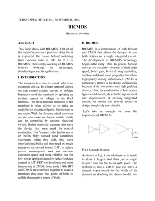
  • 1. TERM PAPER OF ECE-563, NOVEMBER, 2014 BICMOS Himanshu Shekhar ABSTRACT This paper deals with BICMOS. First of all the need of transistor is justified. After this it is explained, the reason behind switching from vacuum tube to BJT to FET to BICMOS. Then simple working of BICMOS inverter working, its advantages, disadvantages and its application. I. INTRODUCTION The transistor is a three terminal, solid state electronic device. In a three terminal device we can control electric current or voltage between two of the terminals by applying an electric current or voltage to the third terminal. This three terminal character of the transistor is what allows us to make an amplifier for electrical signals, like the one in our radio. With the three-terminal transistor we can also make an electric switch, which can be controlled by another electrical switch. Before transistor vacuum tube were the device that were used for control conduction. But Vacuum tube had to warm up before they worked (and sometimes overheated when they did), they were unreliable and bulky and they used too much energy.so we moved toward BJT, to reduce power consumption, area and increase execution speed and more reliable. But for low power application and to reduce leakage current in BJT, FET was developed and most famous one is CMOS. From early 1980s BJT and CMOS are combined together to make a transistor that uses plus point of both to nullify the negative points of both. II. BICMOS BICMOS is a combination of both bipolar and CMOS that allows the designer to use both devices on a single integrated circuit. The development of BICMOS technology began in the early 1980s. In general, bipolar devices are attractive because of their high speed, better gain, better driving capability, and low wideband noise properties that allow high-quality analog performance. CMOS is particularly attractive for digital applications because of its low power and high packing density. Thus, the combination of both device types would not only lead to the replacement and improvement of existing integrated circuit, but would also provide access to design completely new circuits. Let’s take an example to know the importance of BICMOS. Fig.1 Cascade inverter As shown in Fig. 1 cascaded inverter is made to drive a bigger load than just a single inverter, and this has to do with speed. The problem is that a CMOS gate can drive a current proportionally to the width of its channel: so doubling the channel width, we
  • 2. will be able to charge a capacitor twice as fast. If we double the channel width, it also double the input capacitance of the gate, so the stage before will take twice the time to drive the gate. So we need a gate which has the minimum possible input capacitance, while having as much as driving strength as possible. This is obtained cascading several inverters (the most elementary CMOS gate) with increasing channel width, so that the first has the required input capacitance and the last has the required driving strength. In comparison, bipolar junction transistors (BJTs) have more current driving capability, and hence, can overcome such speed bottlenecks using less silicon area. However, the power dissipation of bipolar logic gates is typically one or two orders of magnitude larger than that of comparable CMOS gates. Therefore, such all-bipolar high speed VLSI circuit are difficult to realize and require very elaborate heat-sink arrangements. An alternative solution to the problem of driving large capacitive loads can be provide by merging CMOS and bipolar devices (BICMOS) on chip Taking advantage of the low static power consumption of CMOS and the high current driving capability of the bipolar transistor during transients, the BICMOS configuration The BICMOS combination has significant advantages to offer, such as improved switching speed and less sensitivity with respect to the load capacitance. BICMOS logic circuits are not bipolar-intensive i.e. most logic operations are performed by conventional CMOS sub circuits, while the bipolar transistors are used only when high on-chip or off-chip drive capability is required. III. BASIC BICMOS CIRCUIT In BICMOS inverter as shown in Fig. 2, the complementary pMOS and nMOS transistors MP and MN supply base currents to the bipolar transistor and thus act as a trigger device for bipolar output stage configuration. Depending on the logic level of the input voltage, either MN or MP can be turned on in steady state, therefore assuring a fully complementary push pull operation mode for the two bipolar transistors. In this very simplistic configuration, configuration, two resistors are used to remove the base charge of the bipolar transistors when they are when they are in cut-off mode Fig. 2 Simple BICMOS inverter circuit with resistive base pull-down. The superiority of the BICMOS gate lies in the high current drive capability of the bipolar output transistors, the zero static power dissipation, and the high input impedance provided by the MOSFET configuration. To reduce the turn-off time of the bipolar transistors during switching, Two minimum-size nMOS transistors (MB1 and MB2) are usually added to provide the necessary base Discharge path, instead of the two resistors. As shown in Fig.3
  • 3. Fig. 3 Conventional BICMOS inverter circuit with active base pull-down V. BICMOS INVERTER Consider first the output pull-up transient response, which starts with the input voltage abruptly falling from VOH to VOL at t = 0. The initial condition of the output node voltage is assumed to be VO, = VOH. The inverter circuit during this switching event is depicted in Fig.4, where the active (conducting) devices are highlighted. Fig. 4: BiCMOS inverter during transient output pull-up event. The active devices in thecircuit are highlighted (darker). As the input voltage drops, the pMOS transistor MP is turned on and starts operating in the saturation region. The nMOS transistors MN and MB 1 are turned off; thus, the lower "pull-down" part of the inverter circuit can be ignored except for the corresponding parasitic capacitances of the nMOS transistors and the bipolar transistor Q2. The base pull-down transistor MB2 is turned on, which effectively drains the excess base minority carrier charge of Q2 and assures that Q2 remains in cut-off mode. At the same time, MP is supplying the base current of Q1, which starts to charge up Cload with its emitter current. Now consider the output pull-down transient response, which starts with the input voltage abruptly rising from VOL to VOH at t = 0. The initial condition of the output node voltage is assumed to be Vout = VOL. The inverter circuit during this switching event is depicted in Fig.5, where the active (conducting) devices are highlighted. Fig. 5: BiCMOS inverter during a transient output pull-down event.The active devices in the circuit are highlighted (darker).
  • 4. As the input voltage rises, the pMOS transistor MP is turned off and the nMOS Transistors MN and MB 1 are turned on. The bipolar pull-up transistor Q1 immediately ceases to conduct because its base current drops to zero, and MB 1 starts to remove the excess minority carrier base charge of Q1. The nMOS transistor MN operates initially in the saturation region and supplies the base current of the bipolar pull-down transistor Q2. IV. USES OF BICMOS TECHNOLOGY There have been two significant uses of BICMOS technology. One of the usages is in the design of the high- performance microprocessor unit (MPU) using the high driving capability of bipolar junction transistor because bipolar junction transistor has better transconductance. Comparing the gate delay time and load capacitance capability for same area design, BICMOS has a lower gate delay time than the CMOS at high load capacitive environment as illustrated in Fig 6. Fig. 6 CMOS vs BICMOS And second one is in the mixed signal circuit design, BICMOS design utilizes the excellent analog performance of the double poly self- aligned bipolar junction transistor V. BICMOS APPLICATION 1. In some applications (in which there is finite budget for power) the BICMOS speed performance is better than that of bipolar. 2. This technology is well suited for the intensive input/output applications. 3. The applications of BICMOS were initially in RISC microprocessors rather than traditional CISC microprocessors. 4. It can be used for sample and hold applications as it provides high impedance inputs. 5. This is also used in applications such as adders, mixers, ADC and DAC VI. CONCLUSION The most significant drawback of the BICMOS circuits lies in the increased fabrication process complexity more than that of CMOS. Apart from this it can be used as an alternate of the previous bipolar, ECL and CMOS in the market. VII. REFERENCE [1] http://www.nobelprize.org [2] http://blog.oscarliang.net/bjt-vs-mosfet [3] http:// www.elprocus.com [4] Digital Integrated Circuits, 2/E Jan M. Rabaey, University of California, Berkeley Anantha Chandrakasan, Massachusetts Institute of Technology, Cambridge Borivoje Nikolic, University of California, Berkeley. [5] CMOS Digital integrated Circuits Sung- Mo-Kang & Yusuf Leblebici 3rd 2003 Tata McGraw Hill