3D Integrated Circuits and their economic feasibility
•
5 gostaram•2,091 visualizações

The document discusses 3D integrated circuits (3D ICs) and provides an agenda for a presentation on the topic. The agenda includes an introduction to 3D ICs, advantages of 3D ICs such as reduced timing delay and chip area, challenges in developing 3D IC technology including design tools and manufacturing processes, and business opportunities for 3D ICs in applications like autonomous vehicles, wearables, and smart home devices. Speakers are listed to discuss various aspects of 3D ICs.

Recomendados
Mais conteúdo relacionado
Mais procurados
Mais procurados (20)
Destaque
Destaque (10)
Semelhante a 3D Integrated Circuits and their economic feasibility
Semelhante a 3D Integrated Circuits and their economic feasibility (20)
Mais de Jeffrey Funk
Mais de Jeffrey Funk (20)
Último
Último (20)
3D Integrated Circuits and their economic feasibility
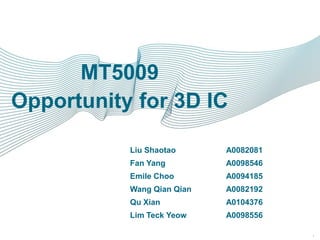
- 1. 1Broadcom Proprietary and Confidential. © 2012 Broadcom Corporation. All rights reserved. Liu Shaotao A0082081 Fan Yang A0098546 Emile Choo A0094185 Wang Qian Qian A0082192 Qu Xian A0104376 Lim Teck Yeow A0098556 MT5009 Opportunity for 3D IC For information on other new technologies that are becoming economically feasible, see http://www.slideshare.net/Funk98/presentations
- 2. 2Broadcom Proprietary and Confidential. © 2012 Broadcom Corporation. All rights reserved. 1.Introduction to 3D IC 2.Advantages of 3D IC 3.Development and Challenges 4.Business opportunities for 3D IC 5.Q&A AGENDA
- 3. 3Broadcom Proprietary and Confidential. © 2012 Broadcom Corporation. All rights reserved. PART1: INTRODUCTION TO 3D IC Liu Shaotao
- 4. 4Broadcom Proprietary and Confidential. © 2012 Broadcom Corporation. All rights reserved. SLOWING DOWN OF MOORE’S LAW
- 5. 5Broadcom Proprietary and Confidential. © 2012 Broadcom Corporation. All rights reserved. CHIP SIZE VS DEVICE SIZE 1953 1983 now 0 50 100 150 200 250 300 350 1971 1972 1974 1978 1982 1985 1992 1994 1995 1998 1999 2000 Chip size year sqmm Device getting smaller Chip size increases
- 6. 6Broadcom Proprietary and Confidential. © 2012 Broadcom Corporation. All rights reserved. WHAT IS 3D IC
- 7. 7Broadcom Proprietary and Confidential. © 2012 Broadcom Corporation. All rights reserved. PART 2: ADVANTAGES OF 3D IC Liu Shaotao
- 8. 8Broadcom Proprietary and Confidential. © 2012 Broadcom Corporation. All rights reserved. Timing delay Length of metal wire connection Data transfer rate Chip area Operating frequency Power consumption Development cost Manufacturing cost KEY PARAMETERS
- 9. 9Broadcom Proprietary and Confidential. © 2012 Broadcom Corporation. All rights reserved. TIMING DELAY: 3D VS 2D 3D ICs Interconnect Performance Modeling and Analysis , Ph.D. Dissertation Draft 3D has 37% reduction Timing delay: - data transfer time from one transistor to another; - smaller timing delay could help to achieve higher frequencies
- 10. 10Broadcom Proprietary and Confidential. © 2012 Broadcom Corporation. All rights reserved. TIMING DELAY: 3D VS 2D (CONTINUE) 3D ICs Interconnect Performance Modeling and Analysis , Ph.D. Dissertation Draft 2 layers: 37% reduction 3 layers: 57% reduction 4 or 5 layers: 65% reduction
- 11. 11Broadcom Proprietary and Confidential. © 2012 Broadcom Corporation. All rights reserved. LENGTH OF METAL WIRE CONNECTION 3D ICs Interconnect Performance Modeling and Analysis , Ph.D. Dissertation Draft 28% and above reduction Metal wire connection: - Length of metal used to connect one transistor to another; -shorter metal wire length help to reduce timing delay and power consumption
- 12. 12Broadcom Proprietary and Confidential. © 2012 Broadcom Corporation. All rights reserved. DATA TRANSFER RATE 3D TECHNOLOGIES: SOME PERSPECTIVES FOR MEMORY INTERCONNECT AND CONTROLLER, Denis Dutoit, Fabien Clermidy, Pascal Vivet 3D IC Cost per 100GB: DDR@16W 3D IC@3.2 W, 80% reduction 2D IC Date transfer rate: - ability to transfer date per second GB/s
- 13. 13Broadcom Proprietary and Confidential. © 2012 Broadcom Corporation. All rights reserved. CHIP AREA 3D ICs Interconnect Performance Modeling and Analysis , Ph.D. Dissertation Draft Chip area: - size of silicon chip 3D IC has 50% reduction
- 14. 14Broadcom Proprietary and Confidential. © 2012 Broadcom Corporation. All rights reserved. OPERATING FREQUENCY 3D ICs Interconnect Performance Modeling and Analysis , Ph.D. Dissertation Draft Operating frequency: - measures the speed of clock; the higher the better
- 15. 15Broadcom Proprietary and Confidential. © 2012 Broadcom Corporation. All rights reserved. ENERGY CONSUMPTION 3D IC technology, Pouya Dormiani and Christopher Lucas 2 layers: 30% reduction 3 layers: 35% reduction 4 or 5 layers: 40% reduction
- 16. 16Broadcom Proprietary and Confidential. © 2012 Broadcom Corporation. All rights reserved. DEVELOPMENT COST http://www.monolithic3d.com/why-monolithic-3d.html
- 17. 17Broadcom Proprietary and Confidential. © 2012 Broadcom Corporation. All rights reserved. MANUFACTURING COST REDUCTION Market trends & Cost analysis for 3D ICs, JC Eloy 128Gb: 30% reduction 256Gb: 50% reduction
- 18. 18Broadcom Proprietary and Confidential. © 2012 Broadcom Corporation. All rights reserved. From: http://www.monolithic3d.com/why-monolithic-3d.html 3D PROTOTYPE
- 19. 19Broadcom Proprietary and Confidential. © 2012 Broadcom Corporation. All rights reserved. PART 3: TECHNOLOGY DEVELOPMENT AND CHALLENGES Fan Yang
- 20. 20Broadcom Proprietary and Confidential. © 2012 Broadcom Corporation. All rights reserved. Simple stacked (Same function) 4. DEVELOPMENT AND CHALLENGES
- 21. 21Broadcom Proprietary and Confidential. © 2012 Broadcom Corporation. All rights reserved. Simple stacked (Same function) Medium integration (Logic+Memory)
- 22. 22Broadcom Proprietary and Confidential. © 2012 Broadcom Corporation. All rights reserved. Simple stacked (Same function) Medium integration (Logic+Memory) Multi-function integration (Heterogeneous) 4. DEVELOPMENT AND CHALLENGES
- 23. 23Broadcom Proprietary and Confidential. © 2012 Broadcom Corporation. All rights reserved. 3D IC EDA designDesign Process Packaging Testing Standard TSV process yield Layers bounding and stacking Chip testing Technology standard 4. DEVELOPMENT AND CHALLENGES
- 24. 24Broadcom Proprietary and Confidential. © 2012 Broadcom Corporation. All rights reserved. Design 2D Design 3D Design Challenges Most EDA IC design tools is not capable for interlayer layout design and simulation. Overall performance, I/O bandwidth, thermal performance is critical 4. DEVELOPMENT AND CHALLENGES Overcome Approches Main stream EDA tools companies like Cadence and Synopsis are dedicated to develop better tools for 3D IC.
- 25. 25Broadcom Proprietary and Confidential. © 2012 Broadcom Corporation. All rights reserved. Process Challenges Through Silicon Via (TSV) yield is the most critical part in process High depth/wide ratio may induce void in TSV Overcome Approaches Leading foundries like TSMC, Samsung, Global foundries, UMC are dedicated in optimize TSV process TSV Void 4. DEVELOPMENT AND CHALLENGES
- 26. 26Broadcom Proprietary and Confidential. © 2012 Broadcom Corporation. All rights reserved. Packaging Micro bump 4. DEVELOPMENT AND CHALLENGES Challenges Interlayer TSV contact quality Interlayer stacking and bonding Overcome Approaches Leading packaging companies like ASE, Amkor, STATS Chip PAC are dedicated in optimize 3D IC packaging technology and process
- 27. 27Broadcom Proprietary and Confidential. © 2012 Broadcom Corporation. All rights reserved. Testing Challenges High integration density, hard to test by normal contact test key. Test individual layer and whole system is reliable, but slow and expensive. Test whole system is economical, but hard to determine failure. Overcome Approaches Design self test and diagnose function in 3D IC design Develop new testing tool and platform to work with 3D IC design Test each layer Test whole system OR
- 28. 28Broadcom Proprietary and Confidential. © 2012 Broadcom Corporation. All rights reserved. Standard Challenge Standard is essential for 3D IC to enter volume production Overcome Approaches Setup technology standard to guide and regulate 3D IC industry 4. DEVELOPMENT AND CHALLENGES
- 29. 29Broadcom Proprietary and Confidential. © 2012 Broadcom Corporation. All rights reserved. PART 4: BUSINESS OPPORTUNITIES FOR 3D IC Emile Choo
- 30. 30Broadcom Proprietary and Confidential. © 2012 Broadcom Corporation. All rights reserved.
- 31. 31Broadcom Proprietary and Confidential. © 2012 Broadcom Corporation. All rights reserved.
- 32. 32Broadcom Proprietary and Confidential. © 2012 Broadcom Corporation. All rights reserved.
- 33. 33Broadcom Proprietary and Confidential. © 2012 Broadcom Corporation. All rights reserved. Auto-pilot cars FUTURE APPLICATIONS Wearable computers and sensors Future robots
- 34. 34Broadcom Proprietary and Confidential. © 2012 Broadcom Corporation. All rights reserved. FUTURE APPLICATIONS Clothes dryer Self-sterilizing door handle Bath or shower
- 35. 35Broadcom Proprietary and Confidential. © 2012 Broadcom Corporation. All rights reserved.
- 36. 36Broadcom Proprietary and Confidential. © 2012 Broadcom Corporation. All rights reserved. 36 Thank You Q&A