SlideShare uma empresa Scribd logo
1 de 10
PCB Production Introduction
PCB means printed
circuits board or
printed wiring boards.
@ Agile Circuit Co., Ltd All Right Reserved ||www.agipcb.com ||custompcbboards.com
PCB is used to carry the electronic components and provide connection the
parts.
SingleSided
PCB
DoubleSided
PCB
Multilayer
PCB
Rigid
PCB
FlexPCB
Rigidand
flexPCB
PTHPCB
Buriedvia
PCB
Blindvia
PCB
HALPCB
Cartonmask
PCB
Goldconnector
PCB
ImmersionGo
PCB
Platinggold
PCB
ENTEK
PCB
By
Hardness
PCB TypesPCB Types
By Hole Depth
Fabrication and
Customer RequirementsBy
Contracture
@ Agile Circuit Co., Ltd All Right Reserved ||www.agipcb.com ||custompcbboards.com
PCB Base Structure
Prepreg
Copper Foil
Copper foil thickness : 1/4 oz,1/3oz,1/2oz,1oz,2oz,3oz
etc.
@ Agile Circuit Co., Ltd All Right Reserved ||www.agipcb.com ||custompcbboards.com
Finished PCB
As picture below :
Solder mask
Annual ring
Screen Marks
PAD
Production Number
3C601
3C6013C601
12658Golden Finger
@ Agile Circuit Co., Ltd All Right Reserved ||www.agipcb.com ||custompcbboards.com
Difference between double side
PCB and multi layer PCB
From the production process :
1. Double-sided PCB lamination with only prepreg and
copper foil. Multilayer PCB with inner core except
prepreg and copper foil.
2. Multilayer PCB is with inner layer production, and
double layer PCB
PCB manufacture| Printed circuit board production| How to make PCB| China PCB house
PCB Base Material Introduction
 There are mainly 3 types divided from TG :
1.TG 130 , the resin consisted by two functional groups℃
Character: low TG, poor heat resistance.
2. TG 140 , the resin is consisted by four functional groups.℃
Character: good heat resistance, good stability, is most commonly used PCB material.
@ Agile Circuit Co., Ltd All Right Reserved ||www.agipcb.com ||custompcbboards.com
3. High TG (TG >150 ), the resin is composed of a plurality of functional groups.℃
Character: TG higher means better heat resistance, but also higher price. The
production process is relatively more complex.
By different related parts :
1. Halogen material
Characters: Most of PCB material used currently is halogen material. It is harmful as it
produces dioxides, dioxin TCDD, dioxin ring cyclohexane when burned, ben
furan and others who with heavy smoke, highly toxic, carcinogenic, once
printed circuit board manufacture|pcb production process|pcb manufacturing|china pcb
intake couldn’t exhaust , will harm to health.
2.Halogen-free material.
Characters: Little proportion of halogen content. According to JPCA-ES-01-2003
standard CL, Br, I content less than 0.09% by weight could call
halogen free material. Due to its harm to human ,relevant laws and
regulations prohibit to use halogen materials for PCB plate (WEEE,
ROHS).
@ Agile Circuit Co., Ltd All Right Reserved ||www.agipcb.com ||custompcbboards.com
PCB Base Material
Introduction
 Divided by solder process
 1. Leaded PCB manufacturing process is with toxic, harmful, reflected in mental
 decline, nausea, headache, insomnia, loss of appetite and so on. Typically is
 anemia, central nervous system disorder.
 2.Leadfree is defined as the lead content <0.1% according to EU. But Japan is
 0.2% as lead-free. It includes the coating of soldering, semiconductor, plated
@ Agile Circuit Co., Ltd All Right Reserved ||www.agipcb.com ||custompcbboards.com
PCB Base Material Introduction
 through hole and PCB pads, stabilizers and related (halogenated resins, wire, paint,
 dye, glass bonding materials etc.)
1)Less toxic to the human body;
2)The melting point of solder material rises (about 217 );℃
3)High requirement on heat resistance of PCB material
4) PCB sheet material requires low DK value, low CET ( before Z-axis expansion
coefficient tg point 50PPM / , after tg 250PPM / ). Normal PCB material sheet℃ ℃
is before TG point 80PPM / , after TG point 300PPM /℃ ℃
@ Agile Circuit Co., Ltd All Right Reserved ||sales@agipcb.com ||custompcbboards.com

Mais conteúdo relacionado

Mais procurados

Double sided PCB manufacturing
Double sided PCB manufacturingDouble sided PCB manufacturing
Double sided PCB manufacturingAditya Todi
 
DFMA guidelines for PCB Design
DFMA guidelines for PCB DesignDFMA guidelines for PCB Design
DFMA guidelines for PCB DesignVihari Andukuri
 
PTH and SMT Component identification and understanding
PTH and SMT Component identification and understandingPTH and SMT Component identification and understanding
PTH and SMT Component identification and understandingsudarshan jadwal
 
PCB designing and Manufacturing
PCB designing and Manufacturing PCB designing and Manufacturing
PCB designing and Manufacturing ManishKenchi
 
pcb layers in layout
pcb layers in layoutpcb layers in layout
pcb layers in layoutAnum Mairaj
 
PCB Process Flow Multilayer Manufacturing Flowchart
PCB Process Flow Multilayer Manufacturing FlowchartPCB Process Flow Multilayer Manufacturing Flowchart
PCB Process Flow Multilayer Manufacturing FlowchartDomestic PCB Fabrication
 
Chapter13 pcb design
Chapter13 pcb designChapter13 pcb design
Chapter13 pcb designVin Voro
 
Printed circuit Board Description
Printed circuit Board DescriptionPrinted circuit Board Description
Printed circuit Board DescriptionRUBY DIKSHIT
 
Surface mount technology(smt)
Surface mount technology(smt)Surface mount technology(smt)
Surface mount technology(smt)AshutoshKumar1262
 

Mais procurados (20)

Double sided PCB manufacturing
Double sided PCB manufacturingDouble sided PCB manufacturing
Double sided PCB manufacturing
 
DFMA guidelines for PCB Design
DFMA guidelines for PCB DesignDFMA guidelines for PCB Design
DFMA guidelines for PCB Design
 
PCB MANUFACTURING
PCB MANUFACTURINGPCB MANUFACTURING
PCB MANUFACTURING
 
SMT
SMTSMT
SMT
 
PTH and SMT Component identification and understanding
PTH and SMT Component identification and understandingPTH and SMT Component identification and understanding
PTH and SMT Component identification and understanding
 
PCB designing and Manufacturing
PCB designing and Manufacturing PCB designing and Manufacturing
PCB designing and Manufacturing
 
pcb layers in layout
pcb layers in layoutpcb layers in layout
pcb layers in layout
 
PCB Process Flow Multilayer Manufacturing Flowchart
PCB Process Flow Multilayer Manufacturing FlowchartPCB Process Flow Multilayer Manufacturing Flowchart
PCB Process Flow Multilayer Manufacturing Flowchart
 
How does your Stack-up, stack up?
How does your Stack-up, stack up?How does your Stack-up, stack up?
How does your Stack-up, stack up?
 
Smt basics
Smt basicsSmt basics
Smt basics
 
PCB Designing
PCB Designing PCB Designing
PCB Designing
 
Pcb design process
Pcb design processPcb design process
Pcb design process
 
OVERVIEW OF IC PACKAGING
OVERVIEW OF IC PACKAGINGOVERVIEW OF IC PACKAGING
OVERVIEW OF IC PACKAGING
 
Chapter13 pcb design
Chapter13 pcb designChapter13 pcb design
Chapter13 pcb design
 
Printed circuit Board Description
Printed circuit Board DescriptionPrinted circuit Board Description
Printed circuit Board Description
 
pcb
pcbpcb
pcb
 
Surface mount technology(smt)
Surface mount technology(smt)Surface mount technology(smt)
Surface mount technology(smt)
 
Pcb design
Pcb designPcb design
Pcb design
 
IC Packaging
IC PackagingIC Packaging
IC Packaging
 
packaging types
packaging typespackaging types
packaging types
 

Destaque

Bare PCB and PCB Assembly Capabilities of OurPCB
Bare PCB and PCB Assembly Capabilities of OurPCBBare PCB and PCB Assembly Capabilities of OurPCB
Bare PCB and PCB Assembly Capabilities of OurPCBMartin Chen
 
PCB Surface Finish
PCB Surface FinishPCB Surface Finish
PCB Surface FinishMark Briggs
 
HKPCA_IPC 2003_BHLee
HKPCA_IPC 2003_BHLeeHKPCA_IPC 2003_BHLee
HKPCA_IPC 2003_BHLeeBH
 
Introduction to PCB Design
Introduction to PCB DesignIntroduction to PCB Design
Introduction to PCB DesignSharan kumar
 
Printed Circuit Board Basics
Printed Circuit Board BasicsPrinted Circuit Board Basics
Printed Circuit Board BasicsSierra Assembly
 
PCB Surface Finishes
PCB Surface FinishesPCB Surface Finishes
PCB Surface FinishesCraig Myers
 
Fundamentals of sdh
Fundamentals of sdhFundamentals of sdh
Fundamentals of sdhsreejithkt
 
Presentation about Fiber Optics
Presentation about Fiber OpticsPresentation about Fiber Optics
Presentation about Fiber OpticsAbidullah Zarghoon
 
OTN for Beginners
OTN for BeginnersOTN for Beginners
OTN for BeginnersMapYourTech
 

Destaque (14)

Bare PCB and PCB Assembly Capabilities of OurPCB
Bare PCB and PCB Assembly Capabilities of OurPCBBare PCB and PCB Assembly Capabilities of OurPCB
Bare PCB and PCB Assembly Capabilities of OurPCB
 
PCB Surface Finish
PCB Surface FinishPCB Surface Finish
PCB Surface Finish
 
HKPCA_IPC 2003_BHLee
HKPCA_IPC 2003_BHLeeHKPCA_IPC 2003_BHLee
HKPCA_IPC 2003_BHLee
 
Pcb layout
Pcb layoutPcb layout
Pcb layout
 
Introduction to PCB Design
Introduction to PCB DesignIntroduction to PCB Design
Introduction to PCB Design
 
Surface Finishes: Why do I need to know more?
Surface Finishes: Why do I need to know more?Surface Finishes: Why do I need to know more?
Surface Finishes: Why do I need to know more?
 
Printed Circuit Board Basics
Printed Circuit Board BasicsPrinted Circuit Board Basics
Printed Circuit Board Basics
 
PCB Surface Finishes
PCB Surface FinishesPCB Surface Finishes
PCB Surface Finishes
 
PCB Layout Fundamentals
PCB Layout FundamentalsPCB Layout Fundamentals
PCB Layout Fundamentals
 
Optical Transport Network
Optical Transport NetworkOptical Transport Network
Optical Transport Network
 
Pcb designing
Pcb designingPcb designing
Pcb designing
 
Fundamentals of sdh
Fundamentals of sdhFundamentals of sdh
Fundamentals of sdh
 
Presentation about Fiber Optics
Presentation about Fiber OpticsPresentation about Fiber Optics
Presentation about Fiber Optics
 
OTN for Beginners
OTN for BeginnersOTN for Beginners
OTN for Beginners
 

Semelhante a PCB Production Introduction /How to Make PCB (1)

Www.raypcb.com tag-copperseparation.html
Www.raypcb.com  tag-copperseparation.htmlWww.raypcb.com  tag-copperseparation.html
Www.raypcb.com tag-copperseparation.htmlgrace cheng
 
Www.raypcb.com tag-circuitboardforled.html
Www.raypcb.com  tag-circuitboardforled.htmlWww.raypcb.com  tag-circuitboardforled.html
Www.raypcb.com tag-circuitboardforled.htmlgrace cheng
 
Www.raypcb.com tag-electroluxdigital.html
Www.raypcb.com  tag-electroluxdigital.htmlWww.raypcb.com  tag-electroluxdigital.html
Www.raypcb.com tag-electroluxdigital.htmlgrace cheng
 
Www.raypcb.com tag-contaminationprotectforgoldenfingers.html
Www.raypcb.com  tag-contaminationprotectforgoldenfingers.htmlWww.raypcb.com  tag-contaminationprotectforgoldenfingers.html
Www.raypcb.com tag-contaminationprotectforgoldenfingers.htmlgrace cheng
 
Multilayer pcb-supplier-from-pcb-manufacturers
Multilayer pcb-supplier-from-pcb-manufacturersMultilayer pcb-supplier-from-pcb-manufacturers
Multilayer pcb-supplier-from-pcb-manufacturersgrace cheng
 
Www.raypcb.com tag-enamelsmetalsubstratesurfaceprintingprocessisdiscussed.html
Www.raypcb.com  tag-enamelsmetalsubstratesurfaceprintingprocessisdiscussed.htmlWww.raypcb.com  tag-enamelsmetalsubstratesurfaceprintingprocessisdiscussed.html
Www.raypcb.com tag-enamelsmetalsubstratesurfaceprintingprocessisdiscussed.htmlgrace cheng
 
Www.raypcb.com tag-causesofwhitepatchesonpcb.html
Www.raypcb.com  tag-causesofwhitepatchesonpcb.htmlWww.raypcb.com  tag-causesofwhitepatchesonpcb.html
Www.raypcb.com tag-causesofwhitepatchesonpcb.htmlgrace cheng
 
Www.raypcb.com tag-blackberrypcbboard.html
Www.raypcb.com  tag-blackberrypcbboard.htmlWww.raypcb.com  tag-blackberrypcbboard.html
Www.raypcb.com tag-blackberrypcbboard.htmlgrace cheng
 
Www.raypcb.com tag-blackberrypcbboard.html
Www.raypcb.com  tag-blackberrypcbboard.htmlWww.raypcb.com  tag-blackberrypcbboard.html
Www.raypcb.com tag-blackberrypcbboard.htmlgrace cheng
 
Www.raypcb.com tag-electronicassemblyofthebasicrequirementsoflead.html
Www.raypcb.com  tag-electronicassemblyofthebasicrequirementsoflead.htmlWww.raypcb.com  tag-electronicassemblyofthebasicrequirementsoflead.html
Www.raypcb.com tag-electronicassemblyofthebasicrequirementsoflead.htmlgrace cheng
 
Www.raypcb.com tag-cuelectroplatingrelatedtohdipcbfabrication.html
Www.raypcb.com  tag-cuelectroplatingrelatedtohdipcbfabrication.htmlWww.raypcb.com  tag-cuelectroplatingrelatedtohdipcbfabrication.html
Www.raypcb.com tag-cuelectroplatingrelatedtohdipcbfabrication.htmlgrace cheng
 
Www.raypcb.com tag-doublesidepcbchina.html
Www.raypcb.com  tag-doublesidepcbchina.htmlWww.raypcb.com  tag-doublesidepcbchina.html
Www.raypcb.com tag-doublesidepcbchina.htmlgrace cheng
 
Www.raypcb.com tag-copperqualitycontrol.html
Www.raypcb.com  tag-copperqualitycontrol.htmlWww.raypcb.com  tag-copperqualitycontrol.html
Www.raypcb.com tag-copperqualitycontrol.htmlgrace cheng
 
Www.raypcb.com tag-convertfromcupricchloridetocoppersulphate.html
Www.raypcb.com  tag-convertfromcupricchloridetocoppersulphate.htmlWww.raypcb.com  tag-convertfromcupricchloridetocoppersulphate.html
Www.raypcb.com tag-convertfromcupricchloridetocoppersulphate.htmlgrace cheng
 
Www.raypcb.com tag-carbonfilmpcbcommonfaultsandcorrectionmethod.html
Www.raypcb.com  tag-carbonfilmpcbcommonfaultsandcorrectionmethod.htmlWww.raypcb.com  tag-carbonfilmpcbcommonfaultsandcorrectionmethod.html
Www.raypcb.com tag-carbonfilmpcbcommonfaultsandcorrectionmethod.htmlgrace cheng
 
Www.raypcb.com tag-circuitflowsoftware.html
Www.raypcb.com  tag-circuitflowsoftware.htmlWww.raypcb.com  tag-circuitflowsoftware.html
Www.raypcb.com tag-circuitflowsoftware.htmlgrace cheng
 
Www.raypcb.com tag-copperchlorideinindustrialwastewatertreatment.html
Www.raypcb.com  tag-copperchlorideinindustrialwastewatertreatment.htmlWww.raypcb.com  tag-copperchlorideinindustrialwastewatertreatment.html
Www.raypcb.com tag-copperchlorideinindustrialwastewatertreatment.htmlgrace cheng
 
Www.raypcb.com tag-burninboardfabricatorintaiwan.html
Www.raypcb.com  tag-burninboardfabricatorintaiwan.htmlWww.raypcb.com  tag-burninboardfabricatorintaiwan.html
Www.raypcb.com tag-burninboardfabricatorintaiwan.htmlgrace cheng
 
Www.raypcb.com tag-densityprintedcircuitboards.html
Www.raypcb.com  tag-densityprintedcircuitboards.htmlWww.raypcb.com  tag-densityprintedcircuitboards.html
Www.raypcb.com tag-densityprintedcircuitboards.htmlgrace cheng
 
Www.raypcb.com tag-compositionofflexiblefilm.html
Www.raypcb.com  tag-compositionofflexiblefilm.htmlWww.raypcb.com  tag-compositionofflexiblefilm.html
Www.raypcb.com tag-compositionofflexiblefilm.htmlgrace cheng
 

Semelhante a PCB Production Introduction /How to Make PCB (1) (20)

Www.raypcb.com tag-copperseparation.html
Www.raypcb.com  tag-copperseparation.htmlWww.raypcb.com  tag-copperseparation.html
Www.raypcb.com tag-copperseparation.html
 
Www.raypcb.com tag-circuitboardforled.html
Www.raypcb.com  tag-circuitboardforled.htmlWww.raypcb.com  tag-circuitboardforled.html
Www.raypcb.com tag-circuitboardforled.html
 
Www.raypcb.com tag-electroluxdigital.html
Www.raypcb.com  tag-electroluxdigital.htmlWww.raypcb.com  tag-electroluxdigital.html
Www.raypcb.com tag-electroluxdigital.html
 
Www.raypcb.com tag-contaminationprotectforgoldenfingers.html
Www.raypcb.com  tag-contaminationprotectforgoldenfingers.htmlWww.raypcb.com  tag-contaminationprotectforgoldenfingers.html
Www.raypcb.com tag-contaminationprotectforgoldenfingers.html
 
Multilayer pcb-supplier-from-pcb-manufacturers
Multilayer pcb-supplier-from-pcb-manufacturersMultilayer pcb-supplier-from-pcb-manufacturers
Multilayer pcb-supplier-from-pcb-manufacturers
 
Www.raypcb.com tag-enamelsmetalsubstratesurfaceprintingprocessisdiscussed.html
Www.raypcb.com  tag-enamelsmetalsubstratesurfaceprintingprocessisdiscussed.htmlWww.raypcb.com  tag-enamelsmetalsubstratesurfaceprintingprocessisdiscussed.html
Www.raypcb.com tag-enamelsmetalsubstratesurfaceprintingprocessisdiscussed.html
 
Www.raypcb.com tag-causesofwhitepatchesonpcb.html
Www.raypcb.com  tag-causesofwhitepatchesonpcb.htmlWww.raypcb.com  tag-causesofwhitepatchesonpcb.html
Www.raypcb.com tag-causesofwhitepatchesonpcb.html
 
Www.raypcb.com tag-blackberrypcbboard.html
Www.raypcb.com  tag-blackberrypcbboard.htmlWww.raypcb.com  tag-blackberrypcbboard.html
Www.raypcb.com tag-blackberrypcbboard.html
 
Www.raypcb.com tag-blackberrypcbboard.html
Www.raypcb.com  tag-blackberrypcbboard.htmlWww.raypcb.com  tag-blackberrypcbboard.html
Www.raypcb.com tag-blackberrypcbboard.html
 
Www.raypcb.com tag-electronicassemblyofthebasicrequirementsoflead.html
Www.raypcb.com  tag-electronicassemblyofthebasicrequirementsoflead.htmlWww.raypcb.com  tag-electronicassemblyofthebasicrequirementsoflead.html
Www.raypcb.com tag-electronicassemblyofthebasicrequirementsoflead.html
 
Www.raypcb.com tag-cuelectroplatingrelatedtohdipcbfabrication.html
Www.raypcb.com  tag-cuelectroplatingrelatedtohdipcbfabrication.htmlWww.raypcb.com  tag-cuelectroplatingrelatedtohdipcbfabrication.html
Www.raypcb.com tag-cuelectroplatingrelatedtohdipcbfabrication.html
 
Www.raypcb.com tag-doublesidepcbchina.html
Www.raypcb.com  tag-doublesidepcbchina.htmlWww.raypcb.com  tag-doublesidepcbchina.html
Www.raypcb.com tag-doublesidepcbchina.html
 
Www.raypcb.com tag-copperqualitycontrol.html
Www.raypcb.com  tag-copperqualitycontrol.htmlWww.raypcb.com  tag-copperqualitycontrol.html
Www.raypcb.com tag-copperqualitycontrol.html
 
Www.raypcb.com tag-convertfromcupricchloridetocoppersulphate.html
Www.raypcb.com  tag-convertfromcupricchloridetocoppersulphate.htmlWww.raypcb.com  tag-convertfromcupricchloridetocoppersulphate.html
Www.raypcb.com tag-convertfromcupricchloridetocoppersulphate.html
 
Www.raypcb.com tag-carbonfilmpcbcommonfaultsandcorrectionmethod.html
Www.raypcb.com  tag-carbonfilmpcbcommonfaultsandcorrectionmethod.htmlWww.raypcb.com  tag-carbonfilmpcbcommonfaultsandcorrectionmethod.html
Www.raypcb.com tag-carbonfilmpcbcommonfaultsandcorrectionmethod.html
 
Www.raypcb.com tag-circuitflowsoftware.html
Www.raypcb.com  tag-circuitflowsoftware.htmlWww.raypcb.com  tag-circuitflowsoftware.html
Www.raypcb.com tag-circuitflowsoftware.html
 
Www.raypcb.com tag-copperchlorideinindustrialwastewatertreatment.html
Www.raypcb.com  tag-copperchlorideinindustrialwastewatertreatment.htmlWww.raypcb.com  tag-copperchlorideinindustrialwastewatertreatment.html
Www.raypcb.com tag-copperchlorideinindustrialwastewatertreatment.html
 
Www.raypcb.com tag-burninboardfabricatorintaiwan.html
Www.raypcb.com  tag-burninboardfabricatorintaiwan.htmlWww.raypcb.com  tag-burninboardfabricatorintaiwan.html
Www.raypcb.com tag-burninboardfabricatorintaiwan.html
 
Www.raypcb.com tag-densityprintedcircuitboards.html
Www.raypcb.com  tag-densityprintedcircuitboards.htmlWww.raypcb.com  tag-densityprintedcircuitboards.html
Www.raypcb.com tag-densityprintedcircuitboards.html
 
Www.raypcb.com tag-compositionofflexiblefilm.html
Www.raypcb.com  tag-compositionofflexiblefilm.htmlWww.raypcb.com  tag-compositionofflexiblefilm.html
Www.raypcb.com tag-compositionofflexiblefilm.html
 

Último

VIP Call Girls Service Kondapur Hyderabad Call +91-8250192130
VIP Call Girls Service Kondapur Hyderabad Call +91-8250192130VIP Call Girls Service Kondapur Hyderabad Call +91-8250192130
VIP Call Girls Service Kondapur Hyderabad Call +91-8250192130Suhani Kapoor
 
College Call Girls Nashik Nehal 7001305949 Independent Escort Service Nashik
College Call Girls Nashik Nehal 7001305949 Independent Escort Service NashikCollege Call Girls Nashik Nehal 7001305949 Independent Escort Service Nashik
College Call Girls Nashik Nehal 7001305949 Independent Escort Service NashikCall Girls in Nagpur High Profile
 
Call Girls Service Nagpur Tanvi Call 7001035870 Meet With Nagpur Escorts
Call Girls Service Nagpur Tanvi Call 7001035870 Meet With Nagpur EscortsCall Girls Service Nagpur Tanvi Call 7001035870 Meet With Nagpur Escorts
Call Girls Service Nagpur Tanvi Call 7001035870 Meet With Nagpur EscortsCall Girls in Nagpur High Profile
 
Introduction to IEEE STANDARDS and its different types.pptx
Introduction to IEEE STANDARDS and its different types.pptxIntroduction to IEEE STANDARDS and its different types.pptx
Introduction to IEEE STANDARDS and its different types.pptxupamatechverse
 
Software Development Life Cycle By Team Orange (Dept. of Pharmacy)
Software Development Life Cycle By  Team Orange (Dept. of Pharmacy)Software Development Life Cycle By  Team Orange (Dept. of Pharmacy)
Software Development Life Cycle By Team Orange (Dept. of Pharmacy)Suman Mia
 
Coefficient of Thermal Expansion and their Importance.pptx
Coefficient of Thermal Expansion and their Importance.pptxCoefficient of Thermal Expansion and their Importance.pptx
Coefficient of Thermal Expansion and their Importance.pptxAsutosh Ranjan
 
Microscopic Analysis of Ceramic Materials.pptx
Microscopic Analysis of Ceramic Materials.pptxMicroscopic Analysis of Ceramic Materials.pptx
Microscopic Analysis of Ceramic Materials.pptxpurnimasatapathy1234
 
(MEERA) Dapodi Call Girls Just Call 7001035870 [ Cash on Delivery ] Pune Escorts
(MEERA) Dapodi Call Girls Just Call 7001035870 [ Cash on Delivery ] Pune Escorts(MEERA) Dapodi Call Girls Just Call 7001035870 [ Cash on Delivery ] Pune Escorts
(MEERA) Dapodi Call Girls Just Call 7001035870 [ Cash on Delivery ] Pune Escortsranjana rawat
 
(RIA) Call Girls Bhosari ( 7001035870 ) HI-Fi Pune Escorts Service
(RIA) Call Girls Bhosari ( 7001035870 ) HI-Fi Pune Escorts Service(RIA) Call Girls Bhosari ( 7001035870 ) HI-Fi Pune Escorts Service
(RIA) Call Girls Bhosari ( 7001035870 ) HI-Fi Pune Escorts Serviceranjana rawat
 
Call for Papers - African Journal of Biological Sciences, E-ISSN: 2663-2187, ...
Call for Papers - African Journal of Biological Sciences, E-ISSN: 2663-2187, ...Call for Papers - African Journal of Biological Sciences, E-ISSN: 2663-2187, ...
Call for Papers - African Journal of Biological Sciences, E-ISSN: 2663-2187, ...Christo Ananth
 
the ladakh protest in leh ladakh 2024 sonam wangchuk.pptx
the ladakh protest in leh ladakh 2024 sonam wangchuk.pptxthe ladakh protest in leh ladakh 2024 sonam wangchuk.pptx
the ladakh protest in leh ladakh 2024 sonam wangchuk.pptxhumanexperienceaaa
 
(ANVI) Koregaon Park Call Girls Just Call 7001035870 [ Cash on Delivery ] Pun...
(ANVI) Koregaon Park Call Girls Just Call 7001035870 [ Cash on Delivery ] Pun...(ANVI) Koregaon Park Call Girls Just Call 7001035870 [ Cash on Delivery ] Pun...
(ANVI) Koregaon Park Call Girls Just Call 7001035870 [ Cash on Delivery ] Pun...ranjana rawat
 
Porous Ceramics seminar and technical writing
Porous Ceramics seminar and technical writingPorous Ceramics seminar and technical writing
Porous Ceramics seminar and technical writingrakeshbaidya232001
 
VIP Call Girls Service Hitech City Hyderabad Call +91-8250192130
VIP Call Girls Service Hitech City Hyderabad Call +91-8250192130VIP Call Girls Service Hitech City Hyderabad Call +91-8250192130
VIP Call Girls Service Hitech City Hyderabad Call +91-8250192130Suhani Kapoor
 
Sheet Pile Wall Design and Construction: A Practical Guide for Civil Engineer...
Sheet Pile Wall Design and Construction: A Practical Guide for Civil Engineer...Sheet Pile Wall Design and Construction: A Practical Guide for Civil Engineer...
Sheet Pile Wall Design and Construction: A Practical Guide for Civil Engineer...Dr.Costas Sachpazis
 
Booking open Available Pune Call Girls Koregaon Park 6297143586 Call Hot Ind...
Booking open Available Pune Call Girls Koregaon Park  6297143586 Call Hot Ind...Booking open Available Pune Call Girls Koregaon Park  6297143586 Call Hot Ind...
Booking open Available Pune Call Girls Koregaon Park 6297143586 Call Hot Ind...Call Girls in Nagpur High Profile
 
(SHREYA) Chakan Call Girls Just Call 7001035870 [ Cash on Delivery ] Pune Esc...
(SHREYA) Chakan Call Girls Just Call 7001035870 [ Cash on Delivery ] Pune Esc...(SHREYA) Chakan Call Girls Just Call 7001035870 [ Cash on Delivery ] Pune Esc...
(SHREYA) Chakan Call Girls Just Call 7001035870 [ Cash on Delivery ] Pune Esc...ranjana rawat
 

Último (20)

VIP Call Girls Service Kondapur Hyderabad Call +91-8250192130
VIP Call Girls Service Kondapur Hyderabad Call +91-8250192130VIP Call Girls Service Kondapur Hyderabad Call +91-8250192130
VIP Call Girls Service Kondapur Hyderabad Call +91-8250192130
 
College Call Girls Nashik Nehal 7001305949 Independent Escort Service Nashik
College Call Girls Nashik Nehal 7001305949 Independent Escort Service NashikCollege Call Girls Nashik Nehal 7001305949 Independent Escort Service Nashik
College Call Girls Nashik Nehal 7001305949 Independent Escort Service Nashik
 
★ CALL US 9953330565 ( HOT Young Call Girls In Badarpur delhi NCR
★ CALL US 9953330565 ( HOT Young Call Girls In Badarpur delhi NCR★ CALL US 9953330565 ( HOT Young Call Girls In Badarpur delhi NCR
★ CALL US 9953330565 ( HOT Young Call Girls In Badarpur delhi NCR
 
Call Girls Service Nagpur Tanvi Call 7001035870 Meet With Nagpur Escorts
Call Girls Service Nagpur Tanvi Call 7001035870 Meet With Nagpur EscortsCall Girls Service Nagpur Tanvi Call 7001035870 Meet With Nagpur Escorts
Call Girls Service Nagpur Tanvi Call 7001035870 Meet With Nagpur Escorts
 
Introduction to IEEE STANDARDS and its different types.pptx
Introduction to IEEE STANDARDS and its different types.pptxIntroduction to IEEE STANDARDS and its different types.pptx
Introduction to IEEE STANDARDS and its different types.pptx
 
Software Development Life Cycle By Team Orange (Dept. of Pharmacy)
Software Development Life Cycle By  Team Orange (Dept. of Pharmacy)Software Development Life Cycle By  Team Orange (Dept. of Pharmacy)
Software Development Life Cycle By Team Orange (Dept. of Pharmacy)
 
Coefficient of Thermal Expansion and their Importance.pptx
Coefficient of Thermal Expansion and their Importance.pptxCoefficient of Thermal Expansion and their Importance.pptx
Coefficient of Thermal Expansion and their Importance.pptx
 
Microscopic Analysis of Ceramic Materials.pptx
Microscopic Analysis of Ceramic Materials.pptxMicroscopic Analysis of Ceramic Materials.pptx
Microscopic Analysis of Ceramic Materials.pptx
 
(MEERA) Dapodi Call Girls Just Call 7001035870 [ Cash on Delivery ] Pune Escorts
(MEERA) Dapodi Call Girls Just Call 7001035870 [ Cash on Delivery ] Pune Escorts(MEERA) Dapodi Call Girls Just Call 7001035870 [ Cash on Delivery ] Pune Escorts
(MEERA) Dapodi Call Girls Just Call 7001035870 [ Cash on Delivery ] Pune Escorts
 
Call Us -/9953056974- Call Girls In Vikaspuri-/- Delhi NCR
Call Us -/9953056974- Call Girls In Vikaspuri-/- Delhi NCRCall Us -/9953056974- Call Girls In Vikaspuri-/- Delhi NCR
Call Us -/9953056974- Call Girls In Vikaspuri-/- Delhi NCR
 
(RIA) Call Girls Bhosari ( 7001035870 ) HI-Fi Pune Escorts Service
(RIA) Call Girls Bhosari ( 7001035870 ) HI-Fi Pune Escorts Service(RIA) Call Girls Bhosari ( 7001035870 ) HI-Fi Pune Escorts Service
(RIA) Call Girls Bhosari ( 7001035870 ) HI-Fi Pune Escorts Service
 
Call for Papers - African Journal of Biological Sciences, E-ISSN: 2663-2187, ...
Call for Papers - African Journal of Biological Sciences, E-ISSN: 2663-2187, ...Call for Papers - African Journal of Biological Sciences, E-ISSN: 2663-2187, ...
Call for Papers - African Journal of Biological Sciences, E-ISSN: 2663-2187, ...
 
the ladakh protest in leh ladakh 2024 sonam wangchuk.pptx
the ladakh protest in leh ladakh 2024 sonam wangchuk.pptxthe ladakh protest in leh ladakh 2024 sonam wangchuk.pptx
the ladakh protest in leh ladakh 2024 sonam wangchuk.pptx
 
(ANVI) Koregaon Park Call Girls Just Call 7001035870 [ Cash on Delivery ] Pun...
(ANVI) Koregaon Park Call Girls Just Call 7001035870 [ Cash on Delivery ] Pun...(ANVI) Koregaon Park Call Girls Just Call 7001035870 [ Cash on Delivery ] Pun...
(ANVI) Koregaon Park Call Girls Just Call 7001035870 [ Cash on Delivery ] Pun...
 
DJARUM4D - SLOT GACOR ONLINE | SLOT DEMO ONLINE
DJARUM4D - SLOT GACOR ONLINE | SLOT DEMO ONLINEDJARUM4D - SLOT GACOR ONLINE | SLOT DEMO ONLINE
DJARUM4D - SLOT GACOR ONLINE | SLOT DEMO ONLINE
 
Porous Ceramics seminar and technical writing
Porous Ceramics seminar and technical writingPorous Ceramics seminar and technical writing
Porous Ceramics seminar and technical writing
 
VIP Call Girls Service Hitech City Hyderabad Call +91-8250192130
VIP Call Girls Service Hitech City Hyderabad Call +91-8250192130VIP Call Girls Service Hitech City Hyderabad Call +91-8250192130
VIP Call Girls Service Hitech City Hyderabad Call +91-8250192130
 
Sheet Pile Wall Design and Construction: A Practical Guide for Civil Engineer...
Sheet Pile Wall Design and Construction: A Practical Guide for Civil Engineer...Sheet Pile Wall Design and Construction: A Practical Guide for Civil Engineer...
Sheet Pile Wall Design and Construction: A Practical Guide for Civil Engineer...
 
Booking open Available Pune Call Girls Koregaon Park 6297143586 Call Hot Ind...
Booking open Available Pune Call Girls Koregaon Park  6297143586 Call Hot Ind...Booking open Available Pune Call Girls Koregaon Park  6297143586 Call Hot Ind...
Booking open Available Pune Call Girls Koregaon Park 6297143586 Call Hot Ind...
 
(SHREYA) Chakan Call Girls Just Call 7001035870 [ Cash on Delivery ] Pune Esc...
(SHREYA) Chakan Call Girls Just Call 7001035870 [ Cash on Delivery ] Pune Esc...(SHREYA) Chakan Call Girls Just Call 7001035870 [ Cash on Delivery ] Pune Esc...
(SHREYA) Chakan Call Girls Just Call 7001035870 [ Cash on Delivery ] Pune Esc...
 

PCB Production Introduction /How to Make PCB (1)

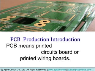
  • 1. PCB Production Introduction PCB means printed circuits board or printed wiring boards. @ Agile Circuit Co., Ltd All Right Reserved ||www.agipcb.com ||custompcbboards.com
  • 2. PCB is used to carry the electronic components and provide connection the parts. SingleSided PCB DoubleSided PCB Multilayer PCB Rigid PCB FlexPCB Rigidand flexPCB PTHPCB Buriedvia PCB Blindvia PCB HALPCB Cartonmask PCB Goldconnector PCB ImmersionGo PCB Platinggold PCB ENTEK PCB By Hardness PCB TypesPCB Types By Hole Depth Fabrication and Customer RequirementsBy Contracture @ Agile Circuit Co., Ltd All Right Reserved ||www.agipcb.com ||custompcbboards.com
  • 3. PCB Base Structure Prepreg Copper Foil Copper foil thickness : 1/4 oz,1/3oz,1/2oz,1oz,2oz,3oz etc. @ Agile Circuit Co., Ltd All Right Reserved ||www.agipcb.com ||custompcbboards.com
  • 4. Finished PCB As picture below : Solder mask Annual ring Screen Marks PAD Production Number 3C601 3C6013C601 12658Golden Finger @ Agile Circuit Co., Ltd All Right Reserved ||www.agipcb.com ||custompcbboards.com
  • 5. Difference between double side PCB and multi layer PCB From the production process : 1. Double-sided PCB lamination with only prepreg and copper foil. Multilayer PCB with inner core except prepreg and copper foil. 2. Multilayer PCB is with inner layer production, and double layer PCB PCB manufacture| Printed circuit board production| How to make PCB| China PCB house
  • 6. PCB Base Material Introduction  There are mainly 3 types divided from TG : 1.TG 130 , the resin consisted by two functional groups℃ Character: low TG, poor heat resistance. 2. TG 140 , the resin is consisted by four functional groups.℃ Character: good heat resistance, good stability, is most commonly used PCB material. @ Agile Circuit Co., Ltd All Right Reserved ||www.agipcb.com ||custompcbboards.com
  • 7. 3. High TG (TG >150 ), the resin is composed of a plurality of functional groups.℃ Character: TG higher means better heat resistance, but also higher price. The production process is relatively more complex. By different related parts : 1. Halogen material Characters: Most of PCB material used currently is halogen material. It is harmful as it produces dioxides, dioxin TCDD, dioxin ring cyclohexane when burned, ben furan and others who with heavy smoke, highly toxic, carcinogenic, once printed circuit board manufacture|pcb production process|pcb manufacturing|china pcb
  • 8. intake couldn’t exhaust , will harm to health. 2.Halogen-free material. Characters: Little proportion of halogen content. According to JPCA-ES-01-2003 standard CL, Br, I content less than 0.09% by weight could call halogen free material. Due to its harm to human ,relevant laws and regulations prohibit to use halogen materials for PCB plate (WEEE, ROHS). @ Agile Circuit Co., Ltd All Right Reserved ||www.agipcb.com ||custompcbboards.com
  • 9. PCB Base Material Introduction  Divided by solder process  1. Leaded PCB manufacturing process is with toxic, harmful, reflected in mental  decline, nausea, headache, insomnia, loss of appetite and so on. Typically is  anemia, central nervous system disorder.  2.Leadfree is defined as the lead content <0.1% according to EU. But Japan is  0.2% as lead-free. It includes the coating of soldering, semiconductor, plated @ Agile Circuit Co., Ltd All Right Reserved ||www.agipcb.com ||custompcbboards.com
  • 10. PCB Base Material Introduction  through hole and PCB pads, stabilizers and related (halogenated resins, wire, paint,  dye, glass bonding materials etc.) 1)Less toxic to the human body; 2)The melting point of solder material rises (about 217 );℃ 3)High requirement on heat resistance of PCB material 4) PCB sheet material requires low DK value, low CET ( before Z-axis expansion coefficient tg point 50PPM / , after tg 250PPM / ). Normal PCB material sheet℃ ℃ is before TG point 80PPM / , after TG point 300PPM /℃ ℃ @ Agile Circuit Co., Ltd All Right Reserved ||sales@agipcb.com ||custompcbboards.com