1. COMMENT
SEPTEMBER 2012 | VOLUME 15 | NUMBER 9358
Making the diamond age a reality
In the past decade, major advancements in the area
of diamond thin film technology have been quietly
taking shape and building a promising case for the
application of diamond thin films in hi-tech products.
This is a major shift for the field, which peaked in
1990s and then slowed down for a long time, due to a
number of technological hurdles. The hurdles include
large area synthesis, high substrate temperatures,
high surface roughness, and difficulties achieving
efficient n-type doping, which ultimately affected
commercial interest in this material. However,
continued academic interest and research in this area
kept the field alive.
In 1998, researchers at Argonne National Laboratory
invented a special form of diamond with very small
grain size (2 – 5 nm), low as-grown roughness
(4 – 7 nm), and high sp3
content (98 %) with
mechanical and tribological properties comparable to
that of single crystal diamond. Argonne researchers
coined the term “ultrananocrystalline diamond”
(UNCD) to name this material because of the small
grain size. Over the years, a number of interesting
properties of UNCD were discovered, such as
semimetallic electrical conductivity (when doped
with boron or incorporated with nitrogen), the lowest
adhesion energy (10 mJ/m2
) and friction coefficient
(0.007) in self-matted configuration, along with a
high hardness (98 GPa) and high Young’s modulus
(980 GPa), and excellent biocompatibility with
resistance to biofouling1,2
. These properties enabled
the development of a number of applications ranging
from the use of UNCD as a robust electrode for water
purification at the macroscale to reusable templates
for the production of nanowires at micro/nanoscales3
.
Also, it could be used as a wear resistant coating
for mechanical face seals at the macroscale4
and
as a wear resistant tip for atomic force microcopy,
for better imaging at the nanoscale5
. The excellent
biocompatible properties of UNCD have now opened
up an entire new field, exploring UNCD coatings not
only for biomedical applications such as bio-implants,
and bio-inert electrodes, but also for developing bio-
sensorstodetectharmfulpathogensinwater.Someof
these applications have already been commercialized
by Advanced Diamond Technologies Inc., which was
founded based on the research carried out at Argonne
on UNCD.
Recent research carried out at the Center for
Nanoscale Materials, Argonne National Laboratory
demonstrated a wafer scale process to deposit
UNCD thin films at 400 °C and its use in developing
complementary metal oxide semiconductor (CMOS)
compatible RF-MEMS switch technology1,6
. In this
case, itwasobservedthatUNCDworks as an excellent
leaky dielectric material, drastically reducing the
dielectric failure that generally occurs with silicon
nitride (used conventionally) due to the build-up of
charge over time. Additionally, a chemically inert
UNCD surface provides low adhesion, reducing
stiction related problems and thus increasing the
performance lifetime of these switches by orders
of magnitude. The low temperature UNCD growth
process developed at CNM was further modified to
increase the grain size from 2 – 5 nm to 100 – 200 nm
by changing the growth chemistry, enhancing the
thermal conductivity of UNCD to a reasonable level7
.
The combination of moderate grain size with lower
deposition temperature allowed direct integration
of UNCD with important semiconductor materials,
such as GaN used in high power electronics for
efficient thermal management7
. With the advances
in chemical mechanical planarization technology, it is
now possible to achieve surface roughness of UNCD
films down to less than a nanometer level eliminating
all problems associated with the high roughness of
diamond films. The low roughness of UNCD films
along with the high thermal conductivity, and low
trap density for charges makes it a unique substrate
material for developing high performance electronic
devices8. Recent research carried out by the company
AKhan Technologies Inc towards achieving n-type
doping in nanocrystalline diamond (NCD) looks
promising.
Looking back on the progress that has been made in
CVD-diamond technology in the last 20 years, it is
clear that the technology is now mature enough and
already making its way towards the market through
some specialized products. One can argue that in
termsof commercial success,diamondthinfilms have
even surpassed other promising carbon materials
such as carbon nanotubes and fullerene. It may not
be an exaggeration to say that the diamond age is not
a distant dream any more but a close reality, that is
just around the corner.
Anirudha V. Sumant | Center for Nanoscale Materials, Argonne National Laboratory | sumant@anl.gov
Ani Sumant considers how after a relatively quiet
period in the field of diamond thin films, this often
overlooked carbon material is making a comeback.
FURTHER READING
1. Sumant et al., MRS Bulletin (2010) 35, 281.
2. Sumant et al., Phys Rev B (2007) 76, 235429.
3. Seley et al., ACS Appl Mater Interfac (2011) 3, 925.
4. Sumant et al., Tribology Transact (2005) 48, 24.
5. Liu et al., Small (2010) 6(10), 1140.
6. Goldsmith et al., IEEE Intl Microwave Symp Dig
(2010), 1246-1249.
7. Goyal et al., Advan Funct Mater (2012) 22(7), 1525.
8. Yu et al., Nano Lett (2012) 12(3), 1603.
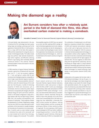
ACMOS wafer with RF-MEMS
switches based on UNCD.