Navigating Complexity: The Role of Trusted Partners and VIAS3D in Dassault Sy...
Original Audio Amplifier IC TDA7850 7850 SIP-25 New ST Microelectronics
1. September 2013 Rev 6 1/18
1
TDA7850
4 x 50 W MOSFET quad bridge power amplifier
Features
■ High output power capability:
– 4 x 50 W/4 max.
– 4 x 30 W/4 @ 14.4 V, 1 kHz, 10 %
– 4 x 80 W/2 max.
– 4 x 55 W/2 @ 14.4V, 1 kHz, 10 %
■ MOSFET output power stage
■ Excellent 2 driving capability
■ Hi-Fi class distortion
■ Low output noise
■ ST-BY function
■ Mute function
■ Automute at min. supply voltage detection
■ Low external component count:
– Internally fixed gain (26 dB)
– No external compensation
– No bootstrap capacitors
■ On board 0.35 A high side driver
Protections:
■ Output short circuit to gnd, to Vs, across the
load
■ Very inductive loads
■ Overrating chip temperature with soft thermal
limiter
■ Output DC offset detection
■ Load dump voltage
■ Fortuitous open gnd
■ Reversed battery
■ ESD
Description
The TDA7850 is a breakthrough MOSFET
technology class AB audio power amplifier in
Flexiwatt 25 package designed for high power car
radio. The fully complementary P-Channel/N-
Channel output structure allows a rail to rail
output voltage swing which, combined with high
output current and minimized saturation losses
sets new power references in the car-radio field,
with unparalleled distortion performances.
The TDA7850 integrates a DC offset detector.
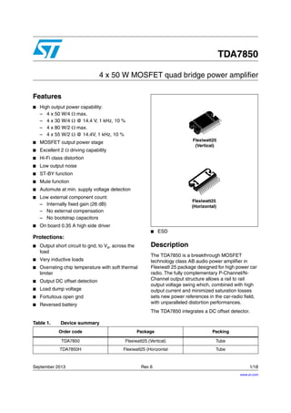
Flexiwatt25
(Vertical)
Flexiwatt25
(Horizontal)
Table 1. Device summary
Order code Package Packing
TDA7850 Flexiwatt25 (Vertical) Tube
TDA7850H Flexiwatt25 (Horizontal Tube
www.st.com
7. TDA7850 Electrical specifications
7/18
3 Electrical specifications
3.1 Absolute maximum ratings
3.2 Thermal data
Table 2. Absolute maximum ratings
Symbol Parameter Value Unit
VS Operating supply voltage 18 V
VS (DC) DC supply voltage 28 V
VS (pk) Peak supply voltage (for t = 50 ms) 50 V
IO
Output peak current
repetitive (duty cycle 10 % at f = 10 Hz)
non repetitive (t = 100 s)
9
10
A
A
Ptot Power dissipation Tcase = 70 °C 80 W
Tj Junction temperature 150 °C
Tstg Storage temperature -55 to 150 °C
Table 3. Thermal data
Symbol Parameter Value Unit
Rth j-case Thermal resistance junction to case Max. 1 °C/W
8. Electrical specifications TDA7850
8/18
3.3 Electrical characteristics
Table 4. Electrical characteristics
(Refer to the test and application diagram, VS = 14.4 V; RL = 4 ; Rg = 600 ; f = 1 kHz;
Tamb = 25 °C; unless otherwise specified).
Symbol Parameter Test condition Min. Typ. Max. Unit
Iq1 Quiescent current RL = 100 180 280 mA
VOS Output offset voltage Play mode / Mute mode ±50 mV
dVOS
During mute ON/OFF output
offset voltage ITU R-ARM weighted
see Figure 20
-10 +10 mV
During Standby ON/OFF output
offset voltage
-10 +10 mV
Gv Voltage gain 25 26 27 dB
dGv Channel gain unbalance ±1 dB
Po Output power
VS = 13.2 V; THD = 10 %
VS = 13.2 V; THD = 1 %
VS = 14.4 V; THD = 10 %
VS = 14.4 V; THD = 1 %
23
16
28
20
25
19
30
23
W
VS = 14.4 V; THD = 10 %, 2 50 55 W
Po max. Max. output power(1) VS = 14.4 V; RL = 4
VS = 14.4 V; RL = 2
50
85
W
THD Distortion
Po = 4W
Po = 15W; RL = 2
0.006
0.015
0.02
0.03
%
eNo Output noise
"A" Weighted
Bw = 20 Hz to 20 kHz
35
50
50
70
V
SVR Supply voltage rejection f = 100 Hz; Vr = 1Vrms 50 75 dB
fch High cut-off frequency PO = 0.5 W 100 300 KHz
Ri Input impedance 80 100 120 K
CT Cross talk
f = 1 kHz PO = 4 W
f = 10 kHz PO = 4 W
60 70
60
-
-
dB
ISB Standby current consumption
VST-BY = 1.5 V 20
A
VST-BY = 0 V 10
Ipin5 ST-BY pin current VST-BY = 1.5 V to 3.5 V ±1 A
VSB out Standby out threshold voltage (Amp: ON) 2.75 V
VSB in Standby in threshold voltage (Amp: OFF) 1.5 V
AM Mute attenuation POref = 4 W 80 90 dB
VM out Mute out threshold voltage (Amp: Play) 3.5 V
VM in Mute in threshold voltage (Amp: Mute) 1.5 V
9. TDA7850 Electrical specifications
9/18
VAM in VS automute threshold
(Amp: Mute)
Att 80 dB; POref = 4 W
(Amp: Play)
Att < 0.1 dB; PO = 0. 5W
6.5 7
7.5 8
V
Ipin23 Muting pin current
VMUTE = 1.5 V
(Sourced Current)
7 12 18 A
VMUTE = 3.5 V -5 18 A
HSD section
Vdropout Dropout voltage IO = 0.35 A; VS = 9 to 16 V 0.25 0.6 V
Iprot Current limits 400 800 mA
Offset detector (Pin 25)
VM_ON Mute voltage for DC offset
detection enabled
VST-BY = 5 V
8 V
VM_OFF 6 V
VOFF Detected differential output offset VST-BY = 5 V; Vmute = 8 V ±2 ±3 ±4 V
V25_T
Pin 25 voltage for detection =
TRUE
VST-BY = 5 V; Vmute = 8 V
VOFF > ±4 V
0 1.5 V
V25_F
Pin 25 Voltage for detection =
FALSE
VST-BY = 5 V; Vmute = 8 V
VOFF > ±2 V
12 V
1. Saturated square wave output.
Table 4. Electrical characteristics (continued)
(Refer to the test and application diagram, VS = 14.4 V; RL = 4 ; Rg = 600 ; f = 1 kHz;
Tamb = 25 °C; unless otherwise specified).
Symbol Parameter Test condition Min. Typ. Max. Unit
11. TDA7850 Electrical specifications
11/18
3.4 Electrical characteristic curves
Figure 6. Quiescent current vs. supply
voltage
Figure 7. Output power vs. supply voltage
(RL = 4)
Figure 8. Output power vs. supply voltage
(RL = 2)
Figure 9. Distortion vs. output power
(RL = 4)
Figure 10. Distortion vs. output power
(RL = 2)
Figure 11. Distortion vs. frequency
(RL = 4)
AC00064
Vs (V)
100
110
120
130
140
150
160
170
180
190
200
8 10 12 14 16 18
Vi = 0
RL =∞
Id (mA)
5
10
15
20
25
30
35
40
45
50
55
60
65
70
75
80
8 9 10 11 12 13 14 15 16 17 18
Po (W)
Vs (V)
RL= 4Ω
f = 1 KHz
Po-max
THD= 10%
THD= 1%
AC00064
AC00066
0
10
20
30
40
50
60
70
80
90
100
110
120
130
8 9 10 11 12 13 14 15 16 17 18
Vs (V)
Po (W)
Po-max
THD=10%
THD=1%
RL= 2Ω
f = 1 KHz
AC00067
0.001
0.01
0.1
1
10
0.1 1 10 100
Po (W)
THD (%)
VS = 14.4 V
RL = 4Ω
f = 1 KHz
f = 10 KHz
AC00068
0.001
0.01
0.1
1
10
0.1 1 10 100
Po (W)
THD (%)
VS = 14.4 V
RL = 2Ω
f = 10 KHz
f = 1 KHz
AC00069
0.001
0.01
0.1
1
10
10 100 1000 10000 100000
f (Hz)
THD (%)
VS = 14.4 V
RL = 4Ω
Po = 4 W
12. Electrical specifications TDA7850
12/18
Figure 12. Distortion vs. frequency
(RL = 2)
Figure 13. Crosstalk vs. frequency
Figure 14. Supply voltage rejection vs.
frequency
Figure 15. Output attenuation vs. supply
voltage
Figure 16. Power dissipation and efficiency
vs. output power (RL = 4, SINE)
Figure 17. Power dissipation and efficiency
vs. output power (RL = 2, SINE)
AC00070
0.001
0.01
0.1
1
10
10 100 1000 10000 100000
f (Hz)
THD (%)
VS = 14.4 V
RL = 2Ω
Po = 8 W
-100
-90
-80
-70
-60
-50
-40
-30
-20
10 100 1000 10000 100000
RL = 4Ω
Po = 4 W
Rg = 600Ω
f (Hz)
CROSSTALK (dB)
AC00071
AC00072
-100
-90
-80
-70
-60
-50
-40
-30
-20
10 100 1000 10000 100000
f (Hz)
SVR (dB)
Rg = 600Ω
Vripple = 1 Vrms
AC00073
-100
-80
-60
-40
-20
0
5 6 7 8 9 10
Vs (V)
OUTPUT ATTN (dB)
RL = 4Ω
Po = 4 W ref
AC00074
0
10
20
30
40
50
60
70
80
90
0 2 4 6 8 10 12 14 16 18 20 22 24 26 28 30
Ptot (W) η (%)
Po (W)
0
10
20
30
40
50
60
70
80
90
Ptot
η
VS = 14.4 V
RL = 4 x 4Ω
f = 1 KHz SINE
AC00075
0
20
40
60
80
100
120
140
160
180
0 5 10 15 20 25 30 35 40 45 50 55
0
10
20
30
40
50
60
70
80
90
Ptot (W) η (%)
Po (W)
Ptot
η
VS = 14.4 V
RL = 4 x 2Ω
f = 1 KHz SINE
13. TDA7850 Electrical specifications
13/18
Figure 18. Power dissipation vs. output power
(RL = 4, audio program simulation)
Figure 19. Power dissipation vs. output power
(RL = 2, audio program simulation)
Figure 20. ITU R-ARM frequency response,
weighting filter for transient pop
AC00076
5
10
15
20
25
30
0 1 2 3 4 5 6
VS = 13.2 V
RL = 4 x 4Ω
GAUSSIAN NOISE
CLIP START
Ptot (W)
Po (W) AC00077
5
10
15
20
25
30
35
40
45
50
55
60
0 2 4 6 8 10
VS = 13.2 V
RL = 4 x 2Ω
GAUSSIAN NOISE
CLIP START
Ptot (W)
Po (W)
Output attenuation (dB)
-50
-40
-30
-20
-10
0
10
10 100 1000 10000 100000
Hz AC00343
14. Application hints TDA7850
14/18
4 Application hints
Referred to the circuit of Figure 2.
4.1 SVR
Besides its contribution to the ripple rejection, the SVR capacitor governs the turn ON/OFF
time sequence and, consequently, plays an essential role in the pop optimization during
ON/OFF transients. To conveniently serve both needs, Its minimum recommended value
is 10µF.
4.2 Input stage
The TDA7850's inputs are ground-compatible and can stand very high input signals (±
8Vpk) without any performance degradation.
If the standard value for the input capacitors (0.1µF) is adopted, the low frequency cut-off
will amount to 16 Hz.
4.3 Standby and muting
Standby and Muting facilities are both CMOS compatible. In absence of true CMOS ports or
microprocessors, a direct connection to Vs of these two pins is admissible but a 470k
equivalent resistance should be present between the power supply and the muting and
ST-BY pins.
R-C cells have always to be used in order to smooth down the transitions for preventing any
audible transient noises.
About the standby, the time constant to be assigned in order to obtain a virtually pop-free
transition has to be slower than 2.5 V/ms.
4.4 DC offset detector
The TDA7850 integrates a DC offset detector to avoid that an anomalous DC offset on the
inputs of the amplifier may be multiplied by the gain and result in a dangerous large offset on
the outputs which may lead to speakers damage for overheating. The feature is enabled by
the MUTE pin (according to table 3) and works with the amplifier unmuted and with no signal
on the inputs.
The DC offset detection is signaled out on the HSD pin. To ensure the correct functionality of
the Offset Detector it is necessary to connect a pulldown 10 kW resistor between HSD and
ground.
4.5 Heatsink definition
Under normal usage (4 Ohm speakers) the heatsink's thermal requirements have to be
deduced from Figure 18, which reports the simulated power dissipation when real
music/speech programmes are played out. Noise with gaussian-distributed amplitude was
employed for this simulation. Based on that, frequent clipping occurrence (worst-case) will
cause Pdiss = 26 W. Assuming Tamb = 70 °C and TCHIP = 150 °C as boundary conditions, the
heatsink's thermal resistance should be approximately 2°C/W. This would avoid any thermal
shutdown occurrence even after long-term and full-volume operation.
15. TDA7850 Package information
15/18
5 Package information
In order to meet environmental requirements, ST (also) offers these devices in ECOPACK®
packages. ECOPACK®
packages are lead-free. The category of second Level Interconnect
is marked on the package and on the inner box label, in compliance with JEDEC Standard
JESD97. The maximum ratings related to soldering conditions are also marked on the inner
box label.
ECOPACK is an ST trademark. ECOPACK specifications are available at: www.st.com.
Figure 21. Flexiwatt25 (vertical) mechanical data and package dimensions
OUTLINE AND
MECHANICAL DATA
DIM.
mm inch
MIN. TYP. MAX. MIN. TYP. MAX.
A 4.45 4.50 4.65 0.175 0.177 0.183
B 1.80 1.90 2.00 0.070 0.074 0.079
C 1.40 0.055
D 0.75 0.90 1.05 0.029 0.035 0.041
E 0.37 0.39 0.42 0.014 0.015 0.016
F (1) 0.57 0.022
G 0.80 1.00 1.20 0.031 0.040 0.047
G1 23.75 24.00 24.25 0.935 0.945 0.955
H (2) 28.90 29.23 29.30 1.139 1.150 1.153
H1 17.00 0.669
H2 12.80 0.503
H3 0.80 0.031
L (2) 22.07 22.47 22.87 0.869 0.884 0.904
L1 18.57 18.97 19.37 0.731 0.747 0.762
L2 (2) 15.50 15.70 15.90 0.610 0.618 0.626
L3 7.70 7.85 7.95 0.303 0.309 0.313
L4 5 0.197
L5 3.5 0.138
M 3.70 4.00 4.30 0.145 0.157 0.169
M1 3.60 4.00 4.40 0.142 0.157 0.173
N 2.20 0.086
O 2 0.079
R 1.70 0.067
R1 0.5 0.02
R2 0.3 0.12
R3 1.25 0.049
R4 0.50 0.019
V1 3˚ (Typ.)
V 5˚ (T p.)
V2 20˚ (Typ.)
V3 45˚ (Typ.)
(2): molding protusion included
(1): dam-bar protusion not included
Flexiwatt25 (vertical)
H3
R4
G
V
G1
L2
H1
H
F
M1
L
FLEX25ME
V3
OL3L4
H2
R3
N
V2
R
R2
R2
C
B
L1
M
R1
L5 R1 R1
E
D
A
Pin 1
V
V1
V1
7034862
16. Package information TDA7850
16/18
Figure 22. Flexiwatt25 (horizontal) mechanical data and package dimensions
OUTLINE AND
MECHANICAL DATA
DIM.
mm inch
MIN. TYP. MAX. MIN. TYP. MAX.
A 4.45 4.50 4.65 0.175 0.177 0.183
B 1.80 1.90 2.00 0.070 0.074 0.079
C 1.40 0.055
D 2.00 0.079
E 0.37 0.39 0.42 0.014 0.015 0.016
F (1) 0.57 0.022
G 0.75 1.00 1.25 0.029 0.040 0.049
G1 23.70 24.00 24.30 0.933 0.945 0.957
H (2) 28.90 29.23 29.30 1.139 1.150 1.153
H1 17.00 0.669
H2 12.80 0.503
H3 0.80 0.031
L (2) 21.64 22.04 22.44 0.852 0.868 0.883
L1 10.15 10.5 10.85 0.40 0.413 0.427
L2 (2) 15.50 15.70 15.90 0.610 0.618 0.626
L3 7.70 7.85 7.95 0.303 0.309 0.313
L4 5 0.197
L5 5.15 5.45 5.85 0.203 0.214 0.23
L6 1.80 1.95 2.10 0.070 0.077 0.083
M 2.75 3.00 3.50 0.108 0.118 0.138
M1 4.73 0.186
M2 5.61 0.220
N 2.20 0.086
P 3.20 3.50 3.80 0.126 0.138 0.15
R 1.70 0.067
R1 0.50 0.02
R2 0.30 0.12
R3 1.25 0.049
R4 0.50 0.02
V 5 (Typ.)
V1 3 (Typ.)
V2 20 (Typ.)
V3 45 (Typ.)
Flexiwatt25
(Horizontal)
7399733 C
(1): dam-bar protusion not included; (2): molding protusion included
17. TDA7850 Revision history
17/18
6 Revision history
Table 5. Document revision history
Date Revision Changes
22-Nov-2006 1 Initial release.
27-Feb-2007 2 Added Chapter 3.4: Electrical characteristic curves.
09-Oct-2007 3
Updated the values for the dVOS and Iq1 parameters on the Table 4.
Added Figure 20 on page 13.
12-Sep-2008 4
Updated Figure 2: Standard test and application circuit.
Updated Section 4.4: DC offset detector and Section 4.3: Standby
and muting.
Updated the values of VOS and THD parameters on the Table 4.
07-Nov-2008 5
Modified max. values of the THD distortion in Table 4: Electrical
characteristics on page 8.
17-Sep-2013 6 Updated Disclaimer.