Direct digital frequency synthesizer
•Transferir como PPTX, PDF•
8 gostaram•3,772 visualizações


Recomendados
Mais conteúdo relacionado
Mais procurados
Mais procurados (20)
Destaque
Destaque (19)
Semelhante a Direct digital frequency synthesizer
Semelhante a Direct digital frequency synthesizer (20)
Mais de Venkat Malai Avichi
Mais de Venkat Malai Avichi (6)
Último
Último (20)
Direct digital frequency synthesizer
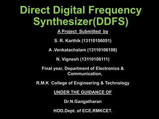
- 1. Direct Digital Frequency Synthesizer(DDFS) A Project Submitted by S. R. Karthik (13110106051) A .Venkatachalam (13110106108) N. Vignesh (13110106111) Final year, Department of Electronics & Communication, R.M.K College of Engineering & Technology UNDER THE GUIDANCE OF Dr.N.Gangatharan HOD,Dept. of ECE,RMKCET.
- 2. Abstract • Direct Digital Synthesis (DDS) is an electronic method for digitally creating arbitrary waveforms from a single, fixed source frequency. • Direct Digital Frequency Synthesis (DDFS) is a mixed signal part i.e. it has both digital and analog parts. • DDFS’s digital part is also known as Numerically Controlled Oscillator (NCO).
- 3. Objective • To understand and analyze the working of a DDFS system . • To create an LUT(look-up-table) for Numerically controlled oscillator(NCO) to aid the optimized wave generation.
- 4. Overview of the project • Introduction • Literature Survey • Existing system • Proposed System • Frequency tuning equations • Numerically Controlled Oscillator(NCO) • Specification of NCO • Tools and system Requirement • Coding and Algorithm • Testing • RTL Schematic • Waveform and simulation • Application • Conclusion • Future work • References
- 5. Introduction • This system was proposed by J.Tierney in the year of 1971. • The output wave form utilizes sampling theory to synthesize. • It consists of NCO as Digital Part ,DAC and RLPF forms the analog part . Frequency control register NCO Reference oscillator DA C Reconstruction LPF N M fclk Analog output
- 6. Literature Survey Title of the Paper Author Inference & Drawback Year of Publication A portable Digitally Controlled Oscillator (DCO) using noval varactors Pao-Lun Cheng, Chen-Yi Lee Implemented the whole problem statement using the Gate- flow logic model and there is no scope for application on a large scale basis May 2011 An Ultra low power and portable DCO for SoC applications Duo- sheng,Ch ing-che Mainly Focusing on reducing noise level and distortion on the output wave and tries to optimize to higher degree at the cost of complex implementations September 2012 ROM-less DDFS system using 16- segment parabolic polynomial interpolation Journal Publishe d by Comput Math Concentration on recent and future development of DDFS is mainly focused. Paved way for a clear understanding of DDFS December 2013
- 7. Existing system • In the existing system, there is no algorithm for improving delay when the value of M is bulky. • The size of the LUT increases as the number of bits n increases.
- 8. Proposed system • In the proposed system we modify the LUT to increase the frequency. • Methods for handling delay and reducing Truncation error is also provided. • The waveform can be varied by varying the LUT variable available in the code.
- 9. Frequency tuning equations • The frequency of the output sine wave is given by fout = (M * fclk )/ 2n . Where n=nth bit and M=forward value. • The output wave will have frequency specified in the range as fout = (∆p * fclk )/2n .
- 10. Numerically Controlled Oscillator • This is a part of DDFS, whose function is vital. • The most scope of the project lies within NCO. • It is a 3rd generation frequency synthesis technology. N-BIT Frequen cy Register N-BIT Phase registe r Sine Look up Tabl e DAC FS W FClk Phase Accumulator NCO O/P Filter
- 11. Specification Of NCO S.No SPECIFICATION PARAMETER VALUES 1. Phase resolution (Bits) 9 2. Spur level(dB) 54.18 3. Frequency Resolution(Bits) 24 4. Output signal Sine & Cosine 5. Output Data Width 9bits Source: IOSR-JVSP volume 1,issue 5(Jan- Feb 2013)
- 12. Tools and System Requirement • System Requirement: PC with minimum Pentium processor and any windows OS platform. • Tools Used: Quartus Model sim simulator version 13.1.0.162.
- 13. Coding and algorithm • We create two modules one for cosine and another one for sine wave . • Same algorithm has been adopted in both the modules, difference lies in the aspect of passing values into the LOOK-UP table. • We pass the input as wire and output as register . • Then once the input are assigned we will create the look up table.
- 14. Continued.. • The values in LUT will get fetched during positive edge of the clock and that may be assigned using Begin statements. • Once the value has been passed and fetched from the LUT we will disable the sine wave by setting acc=0.
- 17. RTL Schematic RTL schematic of NCO along with PA and Delay units
- 18. Waveform and simulation Sine wave been generated at 10KHZ
- 19. Sine wave at frequency less than 10KHZ Continued..
- 22. Application DDFS is mainly used in • Modern communication receivers. • Function generators and Signal Mixers.
- 23. Conclusion • The DDFS models have been successfully created, implemented and simulated using ModelSim simulator. • These models have effectively shown the effect of each building block of the DDFS on the output. • Though the generated waveform is optimized, the LUT could not handle large bits still and complexity increases as n-bit goes up. • Hence that limitation has been taken as a future improvement to reduce delay and complexity for larger bit
- 24. Future work •Since the length of the phase accumulator is long and fetching includes little higher delay we need to optimize it still to a greater extend.
- 25. References • Nehal.A.Ranabhatt,Sudhir Agarwal,Priyesh.P.Gandhi and Raghunandh.k.Bhattar(2013),“Design and implementation of numerically controlled oscillator on FPGA “, Proceedings of IEEE ISSN NO:978-1-4673-599. • DDS Technology- Online Available WWW: http://www.hit.bme.hu/~papay/sci/DDS/start.htm. • “Direct Digital Synthesizers: Theory, Design and Applications”- Jouko Vankka ,Boston London , Kluwer Academic Publishers, 2001 .
- 26. THANK YOU