SlideShare uma empresa Scribd logo
1 de 4
Baixar para ler offline
International Journal of Science and Research (IJSR), India Online ISSN: 2319-7064
Volume 2 Issue 9, September 2013
www.ijsr.net
Design and Analysis of Low Power Implicit Pulse
Triggered Flip-Flops
K. Lovaraju1
, K. Rajendra Prasad2
1
PG Scholar, Department of ECE, Pydah College of Engineering and Technology,
Visakhapatnam, Andhra Pradesh, India
2
Assistant Professor, Department of ECE, Pydah College of Engineering and Technology,
Visakhapatnam, Andhra Pradesh, India
Abstract: In this paper, a novel low-power pulse-triggered flip-flop (P-FF) design is presented. Pulse- triggered FF (P-FF) has been
considered as a popular alternative to the conventional master –slave based FF in the applications of high speed. In particular, digital
designs now-a-days often adopt intensive pipelining techniques and employ many FF-rich Modules. It is also estimated that the power
consumption of the clock system, which consists of clock distribution networks and storage elements, is as high as 20%–45% of the total
system power. First, the pulse generation control logic, an AND function, is removed from the critical path to facilitate a faster
discharge operation. A simple two-transistor AND gate design is used to reduce the circuit complexity. Second, a conditional pulse-
enhancement technique is devised to speed up the discharge along the critical path only when needed. As a result, transistor sizes in
delay inverter and pulse-generation circuit can be reduced for power saving. The simulations are done using Microwind & DSCH
analysis software tools. Our proposed system simulations are done under 50nm technology and the results are compared with other
conventional flip-flops. Hence, our proposed system is showing better output than the other flip-flops.
Keywords: DSCH, Flip-Flop, low power, Microwind, Pulse triggered
1. Introduction
Flip-flops (FFs) are the basic storage elements used
extensively in all kinds of digital designs. In particular,
digital designs now-a-days often adopt intensive pipelining
techniques and employ many FF-rich modules. It is also
estimated that the power consumption of the clock system,
which consists of clock distribution networks and storage
elements, is as high as 20%–45% of the total system power.
Traditional master-slave flip-flops are made up of two
stages, one master and one slave and they are characterized
by their hard-edge property. Alternatively, pulse-triggered
flip-flops reduce the two stages into one stage and are
characterized by the soft edge property. Pulse-triggered FF
(P-FF) has been considered a popular alternative to the
conventional master–slave based FF in the applications of
high-speed operations. Besides the speed advantage, its
circuits simplicity is also beneficial to lowering the power
consumption of the clock tree system. The circuit
complexity of a P-FF is simplified since only one latch, as
opposed to two used in conventional master–slave
configuration, is needed. P-FFs also allow time borrowing
across clock cycle boundaries and feature a zero or even
negative setup time.
Depending on the method of pulse generation, P-FF designs
can be classified as implicit or explicit. In an implicit-type
P-FF, the pulse generator is a built-in logic of the latch
design and no explicit pulse signals are generated. In an
explicit-type PFF, the designs of pulse generator and latch
are separate. Implicit pulse generation is often considered to
be more power efficient than explicit pulse generation.
In this paper, we are presenting a new type of implicit P-FF
with reduced number of transistors which will reduce the
overall power area as well as delay.
2. Analysis of Conventional Implicit-Type P-
FF Designs
A. Implicit Data Close to Output (Ip-DCO)
Ip-DCO is known as the implicit data close to output. It is an
implicit type flip-flop. In this method the pulse is generated
inside the flip-flop. A state-of-the-art P-FF design, named
ip-DCO, is given in Fig.1. It contains an AND logic-based
pulse generator and a semi-dynamic structured latch design.
Semi-Dynamic Flip-Flop is a high performance flip-flop
because of its small delay and simple topology. It is
measured to be one of fastest flip-flops today. The pulse
generator takes complementary and delay skewed clock
signals to generate a transparent window equal in size to the
delay by inverters I1-I3. Two practical problems exist in this
design. First, during the rising edge, nMOS transistors N2
and N3 are turned on. If data remains high, node X will be
discharged on every rising edge of the clock. This leads to a
large switching power. The other problem is that node
controls two larger MOS transistors (P2 and N5). The large
capacitive load to node causes speed and power performance
degradation.
Figure 1: Ip-DCO
Paper ID: 31081303 80
International Journal of Science and Research (IJSR), India Online ISSN: 2319-7064
Volume 2 Issue 9, September 2013
www.ijsr.net
B. Master Hybrid Latch Level Triggered Flip-Flop
(MHLLF)
The improved P-FF design, named Master Hybrid Latch
Level Triggered Flip-flop (MHLLF) shown in fig 2,by
employing a static latch structure. Node X is no longer pre
charged periodically by the clock signal. A weak pull-up
transistor P1 controlled by the FF output signal Q is used to
maintain the node X level at high when Q is zero. This
design eliminates the unnecessary discharging problem at
node X. However, it encounters a longer Data-to-Q (D-to-Q)
delay during “0” to “1” transitions because node X is not
pre-discharged. Larger transistors N3 and N4 are required to
enhance the discharging capability. Another drawback of
this design is that node X becomes floating when output Q
and input Data both equal to “1”. Extra DC power emerges
if node X is drifted from an intact “1”.
Figure 2: MHLLF
C. Single Ended Conditional Capture Energy Recovery
(SCCER)
It is a refined low power P-FF design. SCCER based on a
conditional discharged technique. In this design, a weak pull
up transistor P1 is used to reduce the load capacitance of
node. The discharge path contains nMOS transistors N2 and
N1 connected in series. In order to eliminate superfluous
switching at node, an extra nMOS transistor N3 is
employed. Since N3 is controlled by Q_fdbk, no discharge
occurs if input data remains high. The worst case timing of
this design occurs when input data is “1” and node is
discharged through four transistors in series, i.e., N1 through
N4, while combating with the pull up transistor P1. A
powerful pull-down circuitry is thus needed to ensure node
can be properly discharged. This implies wider N1 and N2
transistors and a longer delay from the delay inverter I1 to
widen the discharge pulse width.
Figure 3: SCCER
D. P-FF with Pulse Control Scheme
This P-FF adopts two measures to overcome the problems
associated with existing P-FF designs. The first one is
reducing the number of nMOS transistors stacked in the
discharging path. The second one is supporting a mechanism
to conditionally enhance the pull down strength when the
input data is “1.” As opposed to the transistor stacking
design in Fig. 1 and Fig. 3, transistor N2 is removed from
the discharging path. Transistor N2, in conjunction with an
additional transistor N3, forms a two-input pass transistor
logic (PTL)-based AND gate to control the discharge of
transistor N1.
Figure 4: P-FF with Pulse Control Scheme
Since the two inputs to the AND logic are mostly
complementary (except during the transition edges of the
clock), the output node Z is kept at zero most of the time.
When both input signals equal to “0” (during the falling
edges of the clock), temporary floating at node Z is basically
harmless. At the rising edges of the clock, both transistors
N2 and N3 are turned on and collaborate to pass a weak
logic high to node Z, which then turns on transistor N1 by a
time span defined by the delay inverter I1. The switching
power at node Z can be reduced due to a diminished voltage
swing. Unlike the MHLLF design, where the discharge
control signal is driven by a single transistor, parallel
conduction of two nMOS transistors (N2 and N3) speeds up
the operations of pulse generation. With this design
measure, the number of stacked transistors along the
discharging path is reduced and the sizes of transistors N1-
N5 can be reduced also. In this design, the longest
discharging path is formed when input data is “1” while the
Qbar output is “1.” To enhance the discharging under this
condition, transistor P3 is added. Transistor P3 is normally
turned off because node X is pulled high most of the time.
This provides additional boost to node Z (from VDD_VTH
to VDD). The generated pulse is taller, which enhances the
pull-down strength of transistor N1. After the rising edge of
the clock, the delay inverter I1 drives node Z back to zero
through transistor N3 to shut down the discharging path.
E. Our Proposed FF Design
By using the Transistor switching logic only we are
designing this circuit so it will be consuming only less
Paper ID: 31081303 81
International Journal of Science and Research (IJSR), India Online ISSN: 2319-7064
Volume 2 Issue 9, September 2013
www.ijsr.net
power when compared to all other circuits. As well as we
are having only 8 Transistors including the not gates also. So
we will be having much reduced power and area when
compared to the other two designs. At the same time due to
the reduced no of transistor count we can reduce the delay
oriented things also. Thus we are reducing the overall
switching delay and power, area consumption.
The figure 5 shows the proposed FF in DSCH. The Layout
design of the proposed new flip-flop is shown in the figure
6. The graph (fig 7) represents the input & output
characteristics of our proposed system from that we can
clearly understand how it works. There is some nanoseconds
delay is there even though it is a negligible amount only.
Those delays can be further reduced by reducing the sizes of
the transistor we are using in this circuit. Or by reducing the
nanometer technology also we can reduce the power
constraints. The Power consumption characteristics are also
shown below in figure 8.
Figure 5: Proposed FF in DSCH
Figure 6: Layout of proposed FF
Figure 7: Input-output characteristics of proposed FF
Figure 8: Power consumption of proposed FF
F. Comparison Table
Type of FF No. of Transistors Power consumption
Ip-DCO 15 14.440 µw
MHLLF 15 0.310 mw
SCCER 13 7.381 µw
P-FF 15 6.981 µw
Proposed FF 10 2.339 µw
3. Conclusion
In this Paper we proposed a new flip flop design which has
only 10 transistors, shows much less power & Area
constraints than the other existing Flip-Flop designs. As well
as the Proposed design will be having very less clock delay
when compared to all other circuits. Thus our proposed
system is having very less power and area constraints which
will lead to improvement in the case implementation in
future mobile devices. This can be much suitable for
application of battery oriented operation for less power and
area. In future we can add some other leakage reduction
techniques and the power can be further reduced.
4. Acknowledgment
The authors thank the Management, the Principal and the
Department of ECE of PYDAH College of Engineering and
Technology, Visakhapatnam, Andhra Pradesh, India for
providing excellent computing facilities and encouragement.
References
[1] J. M. Labaey and M. Pedram, Low Power Design
Methodologies. Norwell, MA: Kluwer, ch.3, 1996.
[2] H. Kawaguchi and T. Sakurai, “A reduced clock-
Swing flip-flop (RCSFF) for 63% power reduction,”
IEEE J. Solid- State Circuits, vol. 33, no. 5, pp. 807–
811, May 1998.
[3] A. G. M. Strollo, D. De Caro, E. Napoli, and N. Petra,
“A novel high speed sense-amplifier-based flip-flop,”
IEEE Trans. Very Large Scale Integr. (VLSI) Syst.,
vol. 13, no. 11, pp. 1266–1274, Nov. 2005.
[4] J. Tschanz, S. Narendra, Z. Chen, S. Borkar, M.
Sachdev, and V. De, “Comparative delay and energy
of single edge-triggered and dual edge triggered pulsed
flip-flops for high-performance microprocessors,” in
Proc. ISPLED, 2001, pp. 207–212.
Paper ID: 31081303 82
International Journal of Science and Research (IJSR), India Online ISSN: 2319-7064
Volume 2 Issue 9, September 2013
www.ijsr.net
[5] F. Klass, C. Amir, A. Das, K. Aingaran, C. Truong,
R.Wang, A. Mehta, R. Heald, and G.Yee, “A
newfamily of semi-dynamic and dynamic flip flops
with embedded logic for high-performance
processors,” IEEE J.Solid-State Circuits, vol. 34, no. 5,
pp. 712–716, May 1999.
[6] S. D. Naffziger, G. Colon-Bonet, T. Fischer, R.
Riedlinger, T. J.Sullivan, and T. Grutkowski, “The
implementation of the Itanium 2microprocessor,”
IEEE J. Solid-State Circuits, vol. 37, no. 11, pp. 1448–
1460, Nov. 2002.
[7] J. Tschanz, S. Narendra, Z. Chen, S. Borkar, M.
Sachdev, and V. De, “Comparative delay and energy
of single edge-triggered and dual edge triggered pulsed
flip-flops for high-performance microprocessors,” in
Proc. ISPLED, 2001, pp. 207–212.
[8] B. Kong, S. Kim, and Y. Jun, “Conditional-capture
Flip-flop for statistical power reduction,” IEEE J.
Solid-State Circuits, vol. 36, no. 8, pp.1263–1271,
Aug. 2001.
[9] S. H. Rasouli, A. Khademzadeh, A. Afzali- Kusha, and
M. Nourani, “Low power single- and Double-edge-
triggered flip-flops for high speed Applications,” Proc.
Inst. Electr. Eng.—Circuits Devices Syst., vol. 152, no.
2, pp. 118–122, Apr. 2005.
[10] N. H .E. Weste and D .Harris, CMOS VLSI Design.
Reading, MA Pearson Education, Inc., 2005.
Author Profile
K. Lovaraju received the Bachelor of Technology
degree in Electronics and Communication Engineering
from Jawaharlal Nehru Technological University,
Kakinada, Andhra Pradesh, India in 2010. He is
Master of Technology degree from the Department of
VLSI Design, at of Pydah College of Engineering and Technology,
Visakhapatnam, Andhra Pradesh, India. His areas of interest
include digital electronics and Low Power VLSI design currently
pursuing
K. Rajendra Prasad received the Bachelor of
Technology degree in Electronics and Communication
Engineering from Jawaharlal Nehru Technological
University, Kakinada, Andhra Pradesh, India in 2009.
He awarded Master of Technology degree from the
Department of Electronics Communicational Engineering from
Jawaharlal Nehru Technological University, Kakinada, Andhra
Pradesh, India in 2011. Present he is working as an Asst. Professor
in Pydah College of Engineering and Technology, Visakhapatnam,
Andhra Pradesh, India. His areas of interest include
Microprocessors, Signal Processing, Image Processing and Low
Power VLSI design.
Paper ID: 31081303 83

Mais conteúdo relacionado

Mais procurados

Area Efficient Pulsed Clocks & Pulsed Latches on Shift Register Tanner
Area Efficient Pulsed Clocks & Pulsed Latches on Shift Register TannerArea Efficient Pulsed Clocks & Pulsed Latches on Shift Register Tanner
Area Efficient Pulsed Clocks & Pulsed Latches on Shift Register TannerIJMTST Journal
 
Design and Analysis of New Modified Feedthrough Logic (MFTL) Circuits Using C...
Design and Analysis of New Modified Feedthrough Logic (MFTL) Circuits Using C...Design and Analysis of New Modified Feedthrough Logic (MFTL) Circuits Using C...
Design and Analysis of New Modified Feedthrough Logic (MFTL) Circuits Using C...IJERA Editor
 
A Low Power Delay Buffer Using Gated Driver Tree
A Low Power Delay Buffer Using Gated Driver TreeA Low Power Delay Buffer Using Gated Driver Tree
A Low Power Delay Buffer Using Gated Driver TreeIOSR Journals
 
A high speed low power consumption d flip flop for high speed phase frequency...
A high speed low power consumption d flip flop for high speed phase frequency...A high speed low power consumption d flip flop for high speed phase frequency...
A high speed low power consumption d flip flop for high speed phase frequency...IAEME Publication
 
A new area and power efficient single edge triggered flip flop structure for ...
A new area and power efficient single edge triggered flip flop structure for ...A new area and power efficient single edge triggered flip flop structure for ...
A new area and power efficient single edge triggered flip flop structure for ...Alexander Decker
 
Spur Reduction Of MB-OFDM UWB System using CMOS Frequency Synthesizer
Spur Reduction Of MB-OFDM UWB System using CMOS Frequency SynthesizerSpur Reduction Of MB-OFDM UWB System using CMOS Frequency Synthesizer
Spur Reduction Of MB-OFDM UWB System using CMOS Frequency SynthesizerIDES Editor
 
IRJET - High Speed Adder with Ultra Low Power Consumption using XOR and XNOR ...
IRJET - High Speed Adder with Ultra Low Power Consumption using XOR and XNOR ...IRJET - High Speed Adder with Ultra Low Power Consumption using XOR and XNOR ...
IRJET - High Speed Adder with Ultra Low Power Consumption using XOR and XNOR ...IRJET Journal
 
A Survey Analysis on CMOS Integrated Circuits with Clock-Gated Logic Structure
A Survey Analysis on CMOS Integrated Circuits with Clock-Gated Logic StructureA Survey Analysis on CMOS Integrated Circuits with Clock-Gated Logic Structure
A Survey Analysis on CMOS Integrated Circuits with Clock-Gated Logic StructureIJERA Editor
 
Pipelining approach
Pipelining approachPipelining approach
Pipelining approachGopinathD17
 
DESIGN OF A HIGH PRECISION, WIDE RANGED ANALOG CLOCK GENERATOR WITH FIELD PRO...
DESIGN OF A HIGH PRECISION, WIDE RANGED ANALOG CLOCK GENERATOR WITH FIELD PRO...DESIGN OF A HIGH PRECISION, WIDE RANGED ANALOG CLOCK GENERATOR WITH FIELD PRO...
DESIGN OF A HIGH PRECISION, WIDE RANGED ANALOG CLOCK GENERATOR WITH FIELD PRO...VLSICS Design
 
Ijmer 46050106
Ijmer 46050106Ijmer 46050106
Ijmer 46050106IJMER
 
A Single-Phase Clock Multiband Low-Power Flexible Divider
A Single-Phase Clock Multiband Low-Power Flexible DividerA Single-Phase Clock Multiband Low-Power Flexible Divider
A Single-Phase Clock Multiband Low-Power Flexible Dividerijsrd.com
 
A Novel Flipflop Topology for High Speed and Area Efficient Logic Structure D...
A Novel Flipflop Topology for High Speed and Area Efficient Logic Structure D...A Novel Flipflop Topology for High Speed and Area Efficient Logic Structure D...
A Novel Flipflop Topology for High Speed and Area Efficient Logic Structure D...IOSR Journals
 

Mais procurados (18)

Area Efficient Pulsed Clocks & Pulsed Latches on Shift Register Tanner
Area Efficient Pulsed Clocks & Pulsed Latches on Shift Register TannerArea Efficient Pulsed Clocks & Pulsed Latches on Shift Register Tanner
Area Efficient Pulsed Clocks & Pulsed Latches on Shift Register Tanner
 
Design and Analysis of New Modified Feedthrough Logic (MFTL) Circuits Using C...
Design and Analysis of New Modified Feedthrough Logic (MFTL) Circuits Using C...Design and Analysis of New Modified Feedthrough Logic (MFTL) Circuits Using C...
Design and Analysis of New Modified Feedthrough Logic (MFTL) Circuits Using C...
 
A Low Power Delay Buffer Using Gated Driver Tree
A Low Power Delay Buffer Using Gated Driver TreeA Low Power Delay Buffer Using Gated Driver Tree
A Low Power Delay Buffer Using Gated Driver Tree
 
A high speed low power consumption d flip flop for high speed phase frequency...
A high speed low power consumption d flip flop for high speed phase frequency...A high speed low power consumption d flip flop for high speed phase frequency...
A high speed low power consumption d flip flop for high speed phase frequency...
 
Is3515091514
Is3515091514Is3515091514
Is3515091514
 
A new area and power efficient single edge triggered flip flop structure for ...
A new area and power efficient single edge triggered flip flop structure for ...A new area and power efficient single edge triggered flip flop structure for ...
A new area and power efficient single edge triggered flip flop structure for ...
 
Spur Reduction Of MB-OFDM UWB System using CMOS Frequency Synthesizer
Spur Reduction Of MB-OFDM UWB System using CMOS Frequency SynthesizerSpur Reduction Of MB-OFDM UWB System using CMOS Frequency Synthesizer
Spur Reduction Of MB-OFDM UWB System using CMOS Frequency Synthesizer
 
SoC Power Reduction
SoC Power ReductionSoC Power Reduction
SoC Power Reduction
 
En34855860
En34855860En34855860
En34855860
 
J42046469
J42046469J42046469
J42046469
 
IRJET - High Speed Adder with Ultra Low Power Consumption using XOR and XNOR ...
IRJET - High Speed Adder with Ultra Low Power Consumption using XOR and XNOR ...IRJET - High Speed Adder with Ultra Low Power Consumption using XOR and XNOR ...
IRJET - High Speed Adder with Ultra Low Power Consumption using XOR and XNOR ...
 
Vlsi power estimation
Vlsi power estimationVlsi power estimation
Vlsi power estimation
 
A Survey Analysis on CMOS Integrated Circuits with Clock-Gated Logic Structure
A Survey Analysis on CMOS Integrated Circuits with Clock-Gated Logic StructureA Survey Analysis on CMOS Integrated Circuits with Clock-Gated Logic Structure
A Survey Analysis on CMOS Integrated Circuits with Clock-Gated Logic Structure
 
Pipelining approach
Pipelining approachPipelining approach
Pipelining approach
 
DESIGN OF A HIGH PRECISION, WIDE RANGED ANALOG CLOCK GENERATOR WITH FIELD PRO...
DESIGN OF A HIGH PRECISION, WIDE RANGED ANALOG CLOCK GENERATOR WITH FIELD PRO...DESIGN OF A HIGH PRECISION, WIDE RANGED ANALOG CLOCK GENERATOR WITH FIELD PRO...
DESIGN OF A HIGH PRECISION, WIDE RANGED ANALOG CLOCK GENERATOR WITH FIELD PRO...
 
Ijmer 46050106
Ijmer 46050106Ijmer 46050106
Ijmer 46050106
 
A Single-Phase Clock Multiband Low-Power Flexible Divider
A Single-Phase Clock Multiband Low-Power Flexible DividerA Single-Phase Clock Multiband Low-Power Flexible Divider
A Single-Phase Clock Multiband Low-Power Flexible Divider
 
A Novel Flipflop Topology for High Speed and Area Efficient Logic Structure D...
A Novel Flipflop Topology for High Speed and Area Efficient Logic Structure D...A Novel Flipflop Topology for High Speed and Area Efficient Logic Structure D...
A Novel Flipflop Topology for High Speed and Area Efficient Logic Structure D...
 

Destaque

Interact 2 trail
Interact 2 trailInteract 2 trail
Interact 2 trailAtul Rana
 
Design and Implementation of combinational circuits in different low power lo...
Design and Implementation of combinational circuits in different low power lo...Design and Implementation of combinational circuits in different low power lo...
Design and Implementation of combinational circuits in different low power lo...iosrjce
 
Low power design-ver_26_mar08
Low power design-ver_26_mar08Low power design-ver_26_mar08
Low power design-ver_26_mar08Obsidian Software
 
Power Analysis for Beginners
Power Analysis for BeginnersPower Analysis for Beginners
Power Analysis for Beginnersgfb1
 
Introduction to Power Analysis
Introduction to Power AnalysisIntroduction to Power Analysis
Introduction to Power AnalysisDaria Bondareva
 

Destaque (6)

Interact 2 trail
Interact 2 trailInteract 2 trail
Interact 2 trail
 
Design and Implementation of combinational circuits in different low power lo...
Design and Implementation of combinational circuits in different low power lo...Design and Implementation of combinational circuits in different low power lo...
Design and Implementation of combinational circuits in different low power lo...
 
Low power design-ver_26_mar08
Low power design-ver_26_mar08Low power design-ver_26_mar08
Low power design-ver_26_mar08
 
Power Analysis for Beginners
Power Analysis for BeginnersPower Analysis for Beginners
Power Analysis for Beginners
 
Introduction to Power Analysis
Introduction to Power AnalysisIntroduction to Power Analysis
Introduction to Power Analysis
 
Flipflop
FlipflopFlipflop
Flipflop
 

Semelhante a Design and Analysis of Low Power Implicit Pulse Triggered Flip-Flops

Low power and high performance detff using common
Low power and high performance detff using commonLow power and high performance detff using common
Low power and high performance detff using commoneSAT Publishing House
 
Design of a Low Power and Area Efficient Flip Flop With Embedded Logic Module
Design of a Low Power and Area Efficient Flip Flop With Embedded Logic ModuleDesign of a Low Power and Area Efficient Flip Flop With Embedded Logic Module
Design of a Low Power and Area Efficient Flip Flop With Embedded Logic Moduleiosrjce
 
Design a Low Power Flip-Flop Based on a Signal Feed-Through Scheme
Design a Low Power Flip-Flop Based on a Signal Feed-Through SchemeDesign a Low Power Flip-Flop Based on a Signal Feed-Through Scheme
Design a Low Power Flip-Flop Based on a Signal Feed-Through SchemeIRJET Journal
 
Low power and high performance detff using common feedback inverter logic
Low power and high performance detff using common feedback inverter logic Low power and high performance detff using common feedback inverter logic
Low power and high performance detff using common feedback inverter logic eSAT Journals
 
A high speed low power consumption d flip flop for high speed phase frequency...
A high speed low power consumption d flip flop for high speed phase frequency...A high speed low power consumption d flip flop for high speed phase frequency...
A high speed low power consumption d flip flop for high speed phase frequency...IAEME Publication
 
Impact of Hybrid Pass-Transistor Logic (HPTL) on Power, Delay and Area in VL...
Impact of Hybrid Pass-Transistor Logic (HPTL) on Power, Delay  and Area in VL...Impact of Hybrid Pass-Transistor Logic (HPTL) on Power, Delay  and Area in VL...
Impact of Hybrid Pass-Transistor Logic (HPTL) on Power, Delay and Area in VL...IJMER
 
A High-Speed, Low Power Consumption Positive Edge Triggered D Flip-Flop for H...
A High-Speed, Low Power Consumption Positive Edge Triggered D Flip-Flop for H...A High-Speed, Low Power Consumption Positive Edge Triggered D Flip-Flop for H...
A High-Speed, Low Power Consumption Positive Edge Triggered D Flip-Flop for H...VLSICS Design
 
DUAL EDGE-TRIGGERED D-TYPE FLIP-FLOP WITH LOW POWER CONSUMPTION
DUAL EDGE-TRIGGERED D-TYPE FLIP-FLOP WITH LOW POWER CONSUMPTIONDUAL EDGE-TRIGGERED D-TYPE FLIP-FLOP WITH LOW POWER CONSUMPTION
DUAL EDGE-TRIGGERED D-TYPE FLIP-FLOP WITH LOW POWER CONSUMPTIONAIRCC Publishing Corporation
 
DUAL EDGE-TRIGGERED D-TYPE FLIP-FLOP WITH LOW POWER CONSUMPTION
DUAL EDGE-TRIGGERED D-TYPE FLIP-FLOP WITH LOW POWER CONSUMPTIONDUAL EDGE-TRIGGERED D-TYPE FLIP-FLOP WITH LOW POWER CONSUMPTION
DUAL EDGE-TRIGGERED D-TYPE FLIP-FLOP WITH LOW POWER CONSUMPTIONijcsit
 
Design of High Speed Phase Frequency Detector in 0.18 μm CMOS Process for PLL...
Design of High Speed Phase Frequency Detector in 0.18 μm CMOS Process for PLL...Design of High Speed Phase Frequency Detector in 0.18 μm CMOS Process for PLL...
Design of High Speed Phase Frequency Detector in 0.18 μm CMOS Process for PLL...Editor IJCATR
 
AREA EFFICIENT 3.3GHZ PHASE LOCKED LOOP WITH FOUR MULTIPLE OUTPUT USING 45NM ...
AREA EFFICIENT 3.3GHZ PHASE LOCKED LOOP WITH FOUR MULTIPLE OUTPUT USING 45NM ...AREA EFFICIENT 3.3GHZ PHASE LOCKED LOOP WITH FOUR MULTIPLE OUTPUT USING 45NM ...
AREA EFFICIENT 3.3GHZ PHASE LOCKED LOOP WITH FOUR MULTIPLE OUTPUT USING 45NM ...VLSICS Design
 
LEAKAGE POWER REDUCTION AND ANALYSIS OF CMOS SEQUENTIAL CIRCUITS
LEAKAGE POWER REDUCTION AND ANALYSIS OF CMOS SEQUENTIAL CIRCUITSLEAKAGE POWER REDUCTION AND ANALYSIS OF CMOS SEQUENTIAL CIRCUITS
LEAKAGE POWER REDUCTION AND ANALYSIS OF CMOS SEQUENTIAL CIRCUITSVLSICS Design
 

Semelhante a Design and Analysis of Low Power Implicit Pulse Triggered Flip-Flops (20)

J044037073
J044037073J044037073
J044037073
 
Bg4301324326
Bg4301324326Bg4301324326
Bg4301324326
 
Low power and high performance detff using common
Low power and high performance detff using commonLow power and high performance detff using common
Low power and high performance detff using common
 
F010624050
F010624050F010624050
F010624050
 
Design of a Low Power and Area Efficient Flip Flop With Embedded Logic Module
Design of a Low Power and Area Efficient Flip Flop With Embedded Logic ModuleDesign of a Low Power and Area Efficient Flip Flop With Embedded Logic Module
Design of a Low Power and Area Efficient Flip Flop With Embedded Logic Module
 
Mp3422592263
Mp3422592263Mp3422592263
Mp3422592263
 
Design a Low Power Flip-Flop Based on a Signal Feed-Through Scheme
Design a Low Power Flip-Flop Based on a Signal Feed-Through SchemeDesign a Low Power Flip-Flop Based on a Signal Feed-Through Scheme
Design a Low Power Flip-Flop Based on a Signal Feed-Through Scheme
 
Ln3420842089
Ln3420842089Ln3420842089
Ln3420842089
 
Low power and high performance detff using common feedback inverter logic
Low power and high performance detff using common feedback inverter logic Low power and high performance detff using common feedback inverter logic
Low power and high performance detff using common feedback inverter logic
 
Ad4101172176
Ad4101172176Ad4101172176
Ad4101172176
 
A high speed low power consumption d flip flop for high speed phase frequency...
A high speed low power consumption d flip flop for high speed phase frequency...A high speed low power consumption d flip flop for high speed phase frequency...
A high speed low power consumption d flip flop for high speed phase frequency...
 
Impact of Hybrid Pass-Transistor Logic (HPTL) on Power, Delay and Area in VL...
Impact of Hybrid Pass-Transistor Logic (HPTL) on Power, Delay  and Area in VL...Impact of Hybrid Pass-Transistor Logic (HPTL) on Power, Delay  and Area in VL...
Impact of Hybrid Pass-Transistor Logic (HPTL) on Power, Delay and Area in VL...
 
A High-Speed, Low Power Consumption Positive Edge Triggered D Flip-Flop for H...
A High-Speed, Low Power Consumption Positive Edge Triggered D Flip-Flop for H...A High-Speed, Low Power Consumption Positive Edge Triggered D Flip-Flop for H...
A High-Speed, Low Power Consumption Positive Edge Triggered D Flip-Flop for H...
 
DUAL EDGE-TRIGGERED D-TYPE FLIP-FLOP WITH LOW POWER CONSUMPTION
DUAL EDGE-TRIGGERED D-TYPE FLIP-FLOP WITH LOW POWER CONSUMPTIONDUAL EDGE-TRIGGERED D-TYPE FLIP-FLOP WITH LOW POWER CONSUMPTION
DUAL EDGE-TRIGGERED D-TYPE FLIP-FLOP WITH LOW POWER CONSUMPTION
 
DUAL EDGE-TRIGGERED D-TYPE FLIP-FLOP WITH LOW POWER CONSUMPTION
DUAL EDGE-TRIGGERED D-TYPE FLIP-FLOP WITH LOW POWER CONSUMPTIONDUAL EDGE-TRIGGERED D-TYPE FLIP-FLOP WITH LOW POWER CONSUMPTION
DUAL EDGE-TRIGGERED D-TYPE FLIP-FLOP WITH LOW POWER CONSUMPTION
 
H33038041
H33038041H33038041
H33038041
 
Design of High Speed Phase Frequency Detector in 0.18 μm CMOS Process for PLL...
Design of High Speed Phase Frequency Detector in 0.18 μm CMOS Process for PLL...Design of High Speed Phase Frequency Detector in 0.18 μm CMOS Process for PLL...
Design of High Speed Phase Frequency Detector in 0.18 μm CMOS Process for PLL...
 
AREA EFFICIENT 3.3GHZ PHASE LOCKED LOOP WITH FOUR MULTIPLE OUTPUT USING 45NM ...
AREA EFFICIENT 3.3GHZ PHASE LOCKED LOOP WITH FOUR MULTIPLE OUTPUT USING 45NM ...AREA EFFICIENT 3.3GHZ PHASE LOCKED LOOP WITH FOUR MULTIPLE OUTPUT USING 45NM ...
AREA EFFICIENT 3.3GHZ PHASE LOCKED LOOP WITH FOUR MULTIPLE OUTPUT USING 45NM ...
 
LEAKAGE POWER REDUCTION AND ANALYSIS OF CMOS SEQUENTIAL CIRCUITS
LEAKAGE POWER REDUCTION AND ANALYSIS OF CMOS SEQUENTIAL CIRCUITSLEAKAGE POWER REDUCTION AND ANALYSIS OF CMOS SEQUENTIAL CIRCUITS
LEAKAGE POWER REDUCTION AND ANALYSIS OF CMOS SEQUENTIAL CIRCUITS
 
Ng2421772180
Ng2421772180Ng2421772180
Ng2421772180
 

Mais de International Journal of Science and Research (IJSR)

Mais de International Journal of Science and Research (IJSR) (20)

Innovations in the Diagnosis and Treatment of Chronic Heart Failure
Innovations in the Diagnosis and Treatment of Chronic Heart FailureInnovations in the Diagnosis and Treatment of Chronic Heart Failure
Innovations in the Diagnosis and Treatment of Chronic Heart Failure
 
Design and implementation of carrier based sinusoidal pwm (bipolar) inverter
Design and implementation of carrier based sinusoidal pwm (bipolar) inverterDesign and implementation of carrier based sinusoidal pwm (bipolar) inverter
Design and implementation of carrier based sinusoidal pwm (bipolar) inverter
 
Polarization effect of antireflection coating for soi material system
Polarization effect of antireflection coating for soi material systemPolarization effect of antireflection coating for soi material system
Polarization effect of antireflection coating for soi material system
 
Image resolution enhancement via multi surface fitting
Image resolution enhancement via multi surface fittingImage resolution enhancement via multi surface fitting
Image resolution enhancement via multi surface fitting
 
Ad hoc networks technical issues on radio links security & qo s
Ad hoc networks technical issues on radio links security & qo sAd hoc networks technical issues on radio links security & qo s
Ad hoc networks technical issues on radio links security & qo s
 
Microstructure analysis of the carbon nano tubes aluminum composite with diff...
Microstructure analysis of the carbon nano tubes aluminum composite with diff...Microstructure analysis of the carbon nano tubes aluminum composite with diff...
Microstructure analysis of the carbon nano tubes aluminum composite with diff...
 
Improving the life of lm13 using stainless spray ii coating for engine applic...
Improving the life of lm13 using stainless spray ii coating for engine applic...Improving the life of lm13 using stainless spray ii coating for engine applic...
Improving the life of lm13 using stainless spray ii coating for engine applic...
 
An overview on development of aluminium metal matrix composites with hybrid r...
An overview on development of aluminium metal matrix composites with hybrid r...An overview on development of aluminium metal matrix composites with hybrid r...
An overview on development of aluminium metal matrix composites with hybrid r...
 
Pesticide mineralization in water using silver nanoparticles incorporated on ...
Pesticide mineralization in water using silver nanoparticles incorporated on ...Pesticide mineralization in water using silver nanoparticles incorporated on ...
Pesticide mineralization in water using silver nanoparticles incorporated on ...
 
Comparative study on computers operated by eyes and brain
Comparative study on computers operated by eyes and brainComparative study on computers operated by eyes and brain
Comparative study on computers operated by eyes and brain
 
T s eliot and the concept of literary tradition and the importance of allusions
T s eliot and the concept of literary tradition and the importance of allusionsT s eliot and the concept of literary tradition and the importance of allusions
T s eliot and the concept of literary tradition and the importance of allusions
 
Effect of select yogasanas and pranayama practices on selected physiological ...
Effect of select yogasanas and pranayama practices on selected physiological ...Effect of select yogasanas and pranayama practices on selected physiological ...
Effect of select yogasanas and pranayama practices on selected physiological ...
 
Grid computing for load balancing strategies
Grid computing for load balancing strategiesGrid computing for load balancing strategies
Grid computing for load balancing strategies
 
A new algorithm to improve the sharing of bandwidth
A new algorithm to improve the sharing of bandwidthA new algorithm to improve the sharing of bandwidth
A new algorithm to improve the sharing of bandwidth
 
Main physical causes of climate change and global warming a general overview
Main physical causes of climate change and global warming   a general overviewMain physical causes of climate change and global warming   a general overview
Main physical causes of climate change and global warming a general overview
 
Performance assessment of control loops
Performance assessment of control loopsPerformance assessment of control loops
Performance assessment of control loops
 
Capital market in bangladesh an overview
Capital market in bangladesh an overviewCapital market in bangladesh an overview
Capital market in bangladesh an overview
 
Faster and resourceful multi core web crawling
Faster and resourceful multi core web crawlingFaster and resourceful multi core web crawling
Faster and resourceful multi core web crawling
 
Extended fuzzy c means clustering algorithm in segmentation of noisy images
Extended fuzzy c means clustering algorithm in segmentation of noisy imagesExtended fuzzy c means clustering algorithm in segmentation of noisy images
Extended fuzzy c means clustering algorithm in segmentation of noisy images
 
Parallel generators of pseudo random numbers with control of calculation errors
Parallel generators of pseudo random numbers with control of calculation errorsParallel generators of pseudo random numbers with control of calculation errors
Parallel generators of pseudo random numbers with control of calculation errors
 

Último

Sensory_Experience_and_Emotional_Resonance_in_Gabriel_Okaras_The_Piano_and_Th...
Sensory_Experience_and_Emotional_Resonance_in_Gabriel_Okaras_The_Piano_and_Th...Sensory_Experience_and_Emotional_Resonance_in_Gabriel_Okaras_The_Piano_and_Th...
Sensory_Experience_and_Emotional_Resonance_in_Gabriel_Okaras_The_Piano_and_Th...Pooja Bhuva
 
FSB Advising Checklist - Orientation 2024
FSB Advising Checklist - Orientation 2024FSB Advising Checklist - Orientation 2024
FSB Advising Checklist - Orientation 2024Elizabeth Walsh
 
Salient Features of India constitution especially power and functions
Salient Features of India constitution especially power and functionsSalient Features of India constitution especially power and functions
Salient Features of India constitution especially power and functionsKarakKing
 
Application orientated numerical on hev.ppt
Application orientated numerical on hev.pptApplication orientated numerical on hev.ppt
Application orientated numerical on hev.pptRamjanShidvankar
 
General Principles of Intellectual Property: Concepts of Intellectual Proper...
General Principles of Intellectual Property: Concepts of Intellectual  Proper...General Principles of Intellectual Property: Concepts of Intellectual  Proper...
General Principles of Intellectual Property: Concepts of Intellectual Proper...Poonam Aher Patil
 
NO1 Top Black Magic Specialist In Lahore Black magic In Pakistan Kala Ilam Ex...
NO1 Top Black Magic Specialist In Lahore Black magic In Pakistan Kala Ilam Ex...NO1 Top Black Magic Specialist In Lahore Black magic In Pakistan Kala Ilam Ex...
NO1 Top Black Magic Specialist In Lahore Black magic In Pakistan Kala Ilam Ex...Amil baba
 
Towards a code of practice for AI in AT.pptx
Towards a code of practice for AI in AT.pptxTowards a code of practice for AI in AT.pptx
Towards a code of practice for AI in AT.pptxJisc
 
Interdisciplinary_Insights_Data_Collection_Methods.pptx
Interdisciplinary_Insights_Data_Collection_Methods.pptxInterdisciplinary_Insights_Data_Collection_Methods.pptx
Interdisciplinary_Insights_Data_Collection_Methods.pptxPooja Bhuva
 
80 ĐỀ THI THỬ TUYỂN SINH TIẾNG ANH VÀO 10 SỞ GD – ĐT THÀNH PHỐ HỒ CHÍ MINH NĂ...
80 ĐỀ THI THỬ TUYỂN SINH TIẾNG ANH VÀO 10 SỞ GD – ĐT THÀNH PHỐ HỒ CHÍ MINH NĂ...80 ĐỀ THI THỬ TUYỂN SINH TIẾNG ANH VÀO 10 SỞ GD – ĐT THÀNH PHỐ HỒ CHÍ MINH NĂ...
80 ĐỀ THI THỬ TUYỂN SINH TIẾNG ANH VÀO 10 SỞ GD – ĐT THÀNH PHỐ HỒ CHÍ MINH NĂ...Nguyen Thanh Tu Collection
 
Jamworks pilot and AI at Jisc (20/03/2024)
Jamworks pilot and AI at Jisc (20/03/2024)Jamworks pilot and AI at Jisc (20/03/2024)
Jamworks pilot and AI at Jisc (20/03/2024)Jisc
 
Jual Obat Aborsi Hongkong ( Asli No.1 ) 085657271886 Obat Penggugur Kandungan...
Jual Obat Aborsi Hongkong ( Asli No.1 ) 085657271886 Obat Penggugur Kandungan...Jual Obat Aborsi Hongkong ( Asli No.1 ) 085657271886 Obat Penggugur Kandungan...
Jual Obat Aborsi Hongkong ( Asli No.1 ) 085657271886 Obat Penggugur Kandungan...ZurliaSoop
 
Single or Multiple melodic lines structure
Single or Multiple melodic lines structureSingle or Multiple melodic lines structure
Single or Multiple melodic lines structuredhanjurrannsibayan2
 
Python Notes for mca i year students osmania university.docx
Python Notes for mca i year students osmania university.docxPython Notes for mca i year students osmania university.docx
Python Notes for mca i year students osmania university.docxRamakrishna Reddy Bijjam
 
On_Translating_a_Tamil_Poem_by_A_K_Ramanujan.pptx
On_Translating_a_Tamil_Poem_by_A_K_Ramanujan.pptxOn_Translating_a_Tamil_Poem_by_A_K_Ramanujan.pptx
On_Translating_a_Tamil_Poem_by_A_K_Ramanujan.pptxPooja Bhuva
 
ICT Role in 21st Century Education & its Challenges.pptx
ICT Role in 21st Century Education & its Challenges.pptxICT Role in 21st Century Education & its Challenges.pptx
ICT Role in 21st Century Education & its Challenges.pptxAreebaZafar22
 
Beyond_Borders_Understanding_Anime_and_Manga_Fandom_A_Comprehensive_Audience_...
Beyond_Borders_Understanding_Anime_and_Manga_Fandom_A_Comprehensive_Audience_...Beyond_Borders_Understanding_Anime_and_Manga_Fandom_A_Comprehensive_Audience_...
Beyond_Borders_Understanding_Anime_and_Manga_Fandom_A_Comprehensive_Audience_...Pooja Bhuva
 
Google Gemini An AI Revolution in Education.pptx
Google Gemini An AI Revolution in Education.pptxGoogle Gemini An AI Revolution in Education.pptx
Google Gemini An AI Revolution in Education.pptxDr. Sarita Anand
 
Graduate Outcomes Presentation Slides - English
Graduate Outcomes Presentation Slides - EnglishGraduate Outcomes Presentation Slides - English
Graduate Outcomes Presentation Slides - Englishneillewis46
 
Holdier Curriculum Vitae (April 2024).pdf
Holdier Curriculum Vitae (April 2024).pdfHoldier Curriculum Vitae (April 2024).pdf
Holdier Curriculum Vitae (April 2024).pdfagholdier
 

Último (20)

Sensory_Experience_and_Emotional_Resonance_in_Gabriel_Okaras_The_Piano_and_Th...
Sensory_Experience_and_Emotional_Resonance_in_Gabriel_Okaras_The_Piano_and_Th...Sensory_Experience_and_Emotional_Resonance_in_Gabriel_Okaras_The_Piano_and_Th...
Sensory_Experience_and_Emotional_Resonance_in_Gabriel_Okaras_The_Piano_and_Th...
 
FSB Advising Checklist - Orientation 2024
FSB Advising Checklist - Orientation 2024FSB Advising Checklist - Orientation 2024
FSB Advising Checklist - Orientation 2024
 
Salient Features of India constitution especially power and functions
Salient Features of India constitution especially power and functionsSalient Features of India constitution especially power and functions
Salient Features of India constitution especially power and functions
 
Application orientated numerical on hev.ppt
Application orientated numerical on hev.pptApplication orientated numerical on hev.ppt
Application orientated numerical on hev.ppt
 
General Principles of Intellectual Property: Concepts of Intellectual Proper...
General Principles of Intellectual Property: Concepts of Intellectual  Proper...General Principles of Intellectual Property: Concepts of Intellectual  Proper...
General Principles of Intellectual Property: Concepts of Intellectual Proper...
 
NO1 Top Black Magic Specialist In Lahore Black magic In Pakistan Kala Ilam Ex...
NO1 Top Black Magic Specialist In Lahore Black magic In Pakistan Kala Ilam Ex...NO1 Top Black Magic Specialist In Lahore Black magic In Pakistan Kala Ilam Ex...
NO1 Top Black Magic Specialist In Lahore Black magic In Pakistan Kala Ilam Ex...
 
Towards a code of practice for AI in AT.pptx
Towards a code of practice for AI in AT.pptxTowards a code of practice for AI in AT.pptx
Towards a code of practice for AI in AT.pptx
 
Interdisciplinary_Insights_Data_Collection_Methods.pptx
Interdisciplinary_Insights_Data_Collection_Methods.pptxInterdisciplinary_Insights_Data_Collection_Methods.pptx
Interdisciplinary_Insights_Data_Collection_Methods.pptx
 
Mehran University Newsletter Vol-X, Issue-I, 2024
Mehran University Newsletter Vol-X, Issue-I, 2024Mehran University Newsletter Vol-X, Issue-I, 2024
Mehran University Newsletter Vol-X, Issue-I, 2024
 
80 ĐỀ THI THỬ TUYỂN SINH TIẾNG ANH VÀO 10 SỞ GD – ĐT THÀNH PHỐ HỒ CHÍ MINH NĂ...
80 ĐỀ THI THỬ TUYỂN SINH TIẾNG ANH VÀO 10 SỞ GD – ĐT THÀNH PHỐ HỒ CHÍ MINH NĂ...80 ĐỀ THI THỬ TUYỂN SINH TIẾNG ANH VÀO 10 SỞ GD – ĐT THÀNH PHỐ HỒ CHÍ MINH NĂ...
80 ĐỀ THI THỬ TUYỂN SINH TIẾNG ANH VÀO 10 SỞ GD – ĐT THÀNH PHỐ HỒ CHÍ MINH NĂ...
 
Jamworks pilot and AI at Jisc (20/03/2024)
Jamworks pilot and AI at Jisc (20/03/2024)Jamworks pilot and AI at Jisc (20/03/2024)
Jamworks pilot and AI at Jisc (20/03/2024)
 
Jual Obat Aborsi Hongkong ( Asli No.1 ) 085657271886 Obat Penggugur Kandungan...
Jual Obat Aborsi Hongkong ( Asli No.1 ) 085657271886 Obat Penggugur Kandungan...Jual Obat Aborsi Hongkong ( Asli No.1 ) 085657271886 Obat Penggugur Kandungan...
Jual Obat Aborsi Hongkong ( Asli No.1 ) 085657271886 Obat Penggugur Kandungan...
 
Single or Multiple melodic lines structure
Single or Multiple melodic lines structureSingle or Multiple melodic lines structure
Single or Multiple melodic lines structure
 
Python Notes for mca i year students osmania university.docx
Python Notes for mca i year students osmania university.docxPython Notes for mca i year students osmania university.docx
Python Notes for mca i year students osmania university.docx
 
On_Translating_a_Tamil_Poem_by_A_K_Ramanujan.pptx
On_Translating_a_Tamil_Poem_by_A_K_Ramanujan.pptxOn_Translating_a_Tamil_Poem_by_A_K_Ramanujan.pptx
On_Translating_a_Tamil_Poem_by_A_K_Ramanujan.pptx
 
ICT Role in 21st Century Education & its Challenges.pptx
ICT Role in 21st Century Education & its Challenges.pptxICT Role in 21st Century Education & its Challenges.pptx
ICT Role in 21st Century Education & its Challenges.pptx
 
Beyond_Borders_Understanding_Anime_and_Manga_Fandom_A_Comprehensive_Audience_...
Beyond_Borders_Understanding_Anime_and_Manga_Fandom_A_Comprehensive_Audience_...Beyond_Borders_Understanding_Anime_and_Manga_Fandom_A_Comprehensive_Audience_...
Beyond_Borders_Understanding_Anime_and_Manga_Fandom_A_Comprehensive_Audience_...
 
Google Gemini An AI Revolution in Education.pptx
Google Gemini An AI Revolution in Education.pptxGoogle Gemini An AI Revolution in Education.pptx
Google Gemini An AI Revolution in Education.pptx
 
Graduate Outcomes Presentation Slides - English
Graduate Outcomes Presentation Slides - EnglishGraduate Outcomes Presentation Slides - English
Graduate Outcomes Presentation Slides - English
 
Holdier Curriculum Vitae (April 2024).pdf
Holdier Curriculum Vitae (April 2024).pdfHoldier Curriculum Vitae (April 2024).pdf
Holdier Curriculum Vitae (April 2024).pdf
 

Design and Analysis of Low Power Implicit Pulse Triggered Flip-Flops

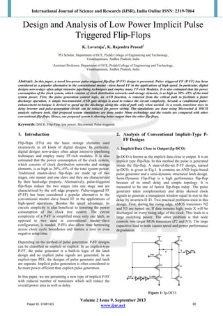
  • 1. International Journal of Science and Research (IJSR), India Online ISSN: 2319-7064 Volume 2 Issue 9, September 2013 www.ijsr.net Design and Analysis of Low Power Implicit Pulse Triggered Flip-Flops K. Lovaraju1 , K. Rajendra Prasad2 1 PG Scholar, Department of ECE, Pydah College of Engineering and Technology, Visakhapatnam, Andhra Pradesh, India 2 Assistant Professor, Department of ECE, Pydah College of Engineering and Technology, Visakhapatnam, Andhra Pradesh, India Abstract: In this paper, a novel low-power pulse-triggered flip-flop (P-FF) design is presented. Pulse- triggered FF (P-FF) has been considered as a popular alternative to the conventional master –slave based FF in the applications of high speed. In particular, digital designs now-a-days often adopt intensive pipelining techniques and employ many FF-rich Modules. It is also estimated that the power consumption of the clock system, which consists of clock distribution networks and storage elements, is as high as 20%–45% of the total system power. First, the pulse generation control logic, an AND function, is removed from the critical path to facilitate a faster discharge operation. A simple two-transistor AND gate design is used to reduce the circuit complexity. Second, a conditional pulse- enhancement technique is devised to speed up the discharge along the critical path only when needed. As a result, transistor sizes in delay inverter and pulse-generation circuit can be reduced for power saving. The simulations are done using Microwind & DSCH analysis software tools. Our proposed system simulations are done under 50nm technology and the results are compared with other conventional flip-flops. Hence, our proposed system is showing better output than the other flip-flops. Keywords: DSCH, Flip-Flop, low power, Microwind, Pulse triggered 1. Introduction Flip-flops (FFs) are the basic storage elements used extensively in all kinds of digital designs. In particular, digital designs now-a-days often adopt intensive pipelining techniques and employ many FF-rich modules. It is also estimated that the power consumption of the clock system, which consists of clock distribution networks and storage elements, is as high as 20%–45% of the total system power. Traditional master-slave flip-flops are made up of two stages, one master and one slave and they are characterized by their hard-edge property. Alternatively, pulse-triggered flip-flops reduce the two stages into one stage and are characterized by the soft edge property. Pulse-triggered FF (P-FF) has been considered a popular alternative to the conventional master–slave based FF in the applications of high-speed operations. Besides the speed advantage, its circuits simplicity is also beneficial to lowering the power consumption of the clock tree system. The circuit complexity of a P-FF is simplified since only one latch, as opposed to two used in conventional master–slave configuration, is needed. P-FFs also allow time borrowing across clock cycle boundaries and feature a zero or even negative setup time. Depending on the method of pulse generation, P-FF designs can be classified as implicit or explicit. In an implicit-type P-FF, the pulse generator is a built-in logic of the latch design and no explicit pulse signals are generated. In an explicit-type PFF, the designs of pulse generator and latch are separate. Implicit pulse generation is often considered to be more power efficient than explicit pulse generation. In this paper, we are presenting a new type of implicit P-FF with reduced number of transistors which will reduce the overall power area as well as delay. 2. Analysis of Conventional Implicit-Type P- FF Designs A. Implicit Data Close to Output (Ip-DCO) Ip-DCO is known as the implicit data close to output. It is an implicit type flip-flop. In this method the pulse is generated inside the flip-flop. A state-of-the-art P-FF design, named ip-DCO, is given in Fig.1. It contains an AND logic-based pulse generator and a semi-dynamic structured latch design. Semi-Dynamic Flip-Flop is a high performance flip-flop because of its small delay and simple topology. It is measured to be one of fastest flip-flops today. The pulse generator takes complementary and delay skewed clock signals to generate a transparent window equal in size to the delay by inverters I1-I3. Two practical problems exist in this design. First, during the rising edge, nMOS transistors N2 and N3 are turned on. If data remains high, node X will be discharged on every rising edge of the clock. This leads to a large switching power. The other problem is that node controls two larger MOS transistors (P2 and N5). The large capacitive load to node causes speed and power performance degradation. Figure 1: Ip-DCO Paper ID: 31081303 80
  • 2. International Journal of Science and Research (IJSR), India Online ISSN: 2319-7064 Volume 2 Issue 9, September 2013 www.ijsr.net B. Master Hybrid Latch Level Triggered Flip-Flop (MHLLF) The improved P-FF design, named Master Hybrid Latch Level Triggered Flip-flop (MHLLF) shown in fig 2,by employing a static latch structure. Node X is no longer pre charged periodically by the clock signal. A weak pull-up transistor P1 controlled by the FF output signal Q is used to maintain the node X level at high when Q is zero. This design eliminates the unnecessary discharging problem at node X. However, it encounters a longer Data-to-Q (D-to-Q) delay during “0” to “1” transitions because node X is not pre-discharged. Larger transistors N3 and N4 are required to enhance the discharging capability. Another drawback of this design is that node X becomes floating when output Q and input Data both equal to “1”. Extra DC power emerges if node X is drifted from an intact “1”. Figure 2: MHLLF C. Single Ended Conditional Capture Energy Recovery (SCCER) It is a refined low power P-FF design. SCCER based on a conditional discharged technique. In this design, a weak pull up transistor P1 is used to reduce the load capacitance of node. The discharge path contains nMOS transistors N2 and N1 connected in series. In order to eliminate superfluous switching at node, an extra nMOS transistor N3 is employed. Since N3 is controlled by Q_fdbk, no discharge occurs if input data remains high. The worst case timing of this design occurs when input data is “1” and node is discharged through four transistors in series, i.e., N1 through N4, while combating with the pull up transistor P1. A powerful pull-down circuitry is thus needed to ensure node can be properly discharged. This implies wider N1 and N2 transistors and a longer delay from the delay inverter I1 to widen the discharge pulse width. Figure 3: SCCER D. P-FF with Pulse Control Scheme This P-FF adopts two measures to overcome the problems associated with existing P-FF designs. The first one is reducing the number of nMOS transistors stacked in the discharging path. The second one is supporting a mechanism to conditionally enhance the pull down strength when the input data is “1.” As opposed to the transistor stacking design in Fig. 1 and Fig. 3, transistor N2 is removed from the discharging path. Transistor N2, in conjunction with an additional transistor N3, forms a two-input pass transistor logic (PTL)-based AND gate to control the discharge of transistor N1. Figure 4: P-FF with Pulse Control Scheme Since the two inputs to the AND logic are mostly complementary (except during the transition edges of the clock), the output node Z is kept at zero most of the time. When both input signals equal to “0” (during the falling edges of the clock), temporary floating at node Z is basically harmless. At the rising edges of the clock, both transistors N2 and N3 are turned on and collaborate to pass a weak logic high to node Z, which then turns on transistor N1 by a time span defined by the delay inverter I1. The switching power at node Z can be reduced due to a diminished voltage swing. Unlike the MHLLF design, where the discharge control signal is driven by a single transistor, parallel conduction of two nMOS transistors (N2 and N3) speeds up the operations of pulse generation. With this design measure, the number of stacked transistors along the discharging path is reduced and the sizes of transistors N1- N5 can be reduced also. In this design, the longest discharging path is formed when input data is “1” while the Qbar output is “1.” To enhance the discharging under this condition, transistor P3 is added. Transistor P3 is normally turned off because node X is pulled high most of the time. This provides additional boost to node Z (from VDD_VTH to VDD). The generated pulse is taller, which enhances the pull-down strength of transistor N1. After the rising edge of the clock, the delay inverter I1 drives node Z back to zero through transistor N3 to shut down the discharging path. E. Our Proposed FF Design By using the Transistor switching logic only we are designing this circuit so it will be consuming only less Paper ID: 31081303 81
  • 3. International Journal of Science and Research (IJSR), India Online ISSN: 2319-7064 Volume 2 Issue 9, September 2013 www.ijsr.net power when compared to all other circuits. As well as we are having only 8 Transistors including the not gates also. So we will be having much reduced power and area when compared to the other two designs. At the same time due to the reduced no of transistor count we can reduce the delay oriented things also. Thus we are reducing the overall switching delay and power, area consumption. The figure 5 shows the proposed FF in DSCH. The Layout design of the proposed new flip-flop is shown in the figure 6. The graph (fig 7) represents the input & output characteristics of our proposed system from that we can clearly understand how it works. There is some nanoseconds delay is there even though it is a negligible amount only. Those delays can be further reduced by reducing the sizes of the transistor we are using in this circuit. Or by reducing the nanometer technology also we can reduce the power constraints. The Power consumption characteristics are also shown below in figure 8. Figure 5: Proposed FF in DSCH Figure 6: Layout of proposed FF Figure 7: Input-output characteristics of proposed FF Figure 8: Power consumption of proposed FF F. Comparison Table Type of FF No. of Transistors Power consumption Ip-DCO 15 14.440 µw MHLLF 15 0.310 mw SCCER 13 7.381 µw P-FF 15 6.981 µw Proposed FF 10 2.339 µw 3. Conclusion In this Paper we proposed a new flip flop design which has only 10 transistors, shows much less power & Area constraints than the other existing Flip-Flop designs. As well as the Proposed design will be having very less clock delay when compared to all other circuits. Thus our proposed system is having very less power and area constraints which will lead to improvement in the case implementation in future mobile devices. This can be much suitable for application of battery oriented operation for less power and area. In future we can add some other leakage reduction techniques and the power can be further reduced. 4. Acknowledgment The authors thank the Management, the Principal and the Department of ECE of PYDAH College of Engineering and Technology, Visakhapatnam, Andhra Pradesh, India for providing excellent computing facilities and encouragement. References [1] J. M. Labaey and M. Pedram, Low Power Design Methodologies. Norwell, MA: Kluwer, ch.3, 1996. [2] H. Kawaguchi and T. Sakurai, “A reduced clock- Swing flip-flop (RCSFF) for 63% power reduction,” IEEE J. Solid- State Circuits, vol. 33, no. 5, pp. 807– 811, May 1998. [3] A. G. M. Strollo, D. De Caro, E. Napoli, and N. Petra, “A novel high speed sense-amplifier-based flip-flop,” IEEE Trans. Very Large Scale Integr. (VLSI) Syst., vol. 13, no. 11, pp. 1266–1274, Nov. 2005. [4] J. Tschanz, S. Narendra, Z. Chen, S. Borkar, M. Sachdev, and V. De, “Comparative delay and energy of single edge-triggered and dual edge triggered pulsed flip-flops for high-performance microprocessors,” in Proc. ISPLED, 2001, pp. 207–212. Paper ID: 31081303 82
  • 4. International Journal of Science and Research (IJSR), India Online ISSN: 2319-7064 Volume 2 Issue 9, September 2013 www.ijsr.net [5] F. Klass, C. Amir, A. Das, K. Aingaran, C. Truong, R.Wang, A. Mehta, R. Heald, and G.Yee, “A newfamily of semi-dynamic and dynamic flip flops with embedded logic for high-performance processors,” IEEE J.Solid-State Circuits, vol. 34, no. 5, pp. 712–716, May 1999. [6] S. D. Naffziger, G. Colon-Bonet, T. Fischer, R. Riedlinger, T. J.Sullivan, and T. Grutkowski, “The implementation of the Itanium 2microprocessor,” IEEE J. Solid-State Circuits, vol. 37, no. 11, pp. 1448– 1460, Nov. 2002. [7] J. Tschanz, S. Narendra, Z. Chen, S. Borkar, M. Sachdev, and V. De, “Comparative delay and energy of single edge-triggered and dual edge triggered pulsed flip-flops for high-performance microprocessors,” in Proc. ISPLED, 2001, pp. 207–212. [8] B. Kong, S. Kim, and Y. Jun, “Conditional-capture Flip-flop for statistical power reduction,” IEEE J. Solid-State Circuits, vol. 36, no. 8, pp.1263–1271, Aug. 2001. [9] S. H. Rasouli, A. Khademzadeh, A. Afzali- Kusha, and M. Nourani, “Low power single- and Double-edge- triggered flip-flops for high speed Applications,” Proc. Inst. Electr. Eng.—Circuits Devices Syst., vol. 152, no. 2, pp. 118–122, Apr. 2005. [10] N. H .E. Weste and D .Harris, CMOS VLSI Design. Reading, MA Pearson Education, Inc., 2005. Author Profile K. Lovaraju received the Bachelor of Technology degree in Electronics and Communication Engineering from Jawaharlal Nehru Technological University, Kakinada, Andhra Pradesh, India in 2010. He is Master of Technology degree from the Department of VLSI Design, at of Pydah College of Engineering and Technology, Visakhapatnam, Andhra Pradesh, India. His areas of interest include digital electronics and Low Power VLSI design currently pursuing K. Rajendra Prasad received the Bachelor of Technology degree in Electronics and Communication Engineering from Jawaharlal Nehru Technological University, Kakinada, Andhra Pradesh, India in 2009. He awarded Master of Technology degree from the Department of Electronics Communicational Engineering from Jawaharlal Nehru Technological University, Kakinada, Andhra Pradesh, India in 2011. Present he is working as an Asst. Professor in Pydah College of Engineering and Technology, Visakhapatnam, Andhra Pradesh, India. His areas of interest include Microprocessors, Signal Processing, Image Processing and Low Power VLSI design. Paper ID: 31081303 83