SlideShare uma empresa Scribd logo
1 de 105
Variable-Frequency Response Analysis
Network performance as function of frequency.
Transfer function
Sinusoidal Frequency Analysis
Bode plots to display frequency response data
Resonant Circuits
The resonance phenomenon and its characterization
Scaling
Impedance and frequency scaling
Filter Networks
Networks with frequency selective characteristics:
low-pass, high-pass, band-pass
VARIABLE-FREQUENCY NETWORK
PERFORMANCE
LEARNING GOALS
°∠== 0RRZRResistor
VARIABLE FREQUENCY-RESPONSE ANALYSIS
In AC steady state analysis the frequency is assumed constant (e.g., 60Hz).
Here we consider the frequency as a variable and examine how the performance
varies with the frequency.
Variation in impedance of basic components
°∠== 90LLjZL ωωInductor
Capacitor °−∠== 90
11
CCj
Zc
ωω
Frequency dependent behavior of series RLC network
Cj
RCjLCj
Cj
LjRZeq
ω
ωω
ω
ω
1)(1 2
++
=++=
C
LCjRC
j
j
ω
ωω )1( 2
−+
=
−
−
×
C
LCRC
Zeq
ω
ωω 222
)1()(
||
−+
= 




 −
=∠ −
RC
LC
Zeq
ω
ω 1
tan
2
1
sC
sRCLCs
sZ
sj
eq
1
)(
2
++
=
≈ωnotation"intionSimplifica"
For all cases seen, and all cases to be studied, the impedance is of the form
01
1
1
01
1
1
...
...
)(
bsbsbsb
asasasa
sZ n
n
n
n
m
m
m
m
++++
++++
= −
−
−
−
sC
ZsLsZRsZ CLR
1
,)(,)( ===
Simplified notation for basic components
Moreover, if the circuit elements (L,R,C, dependent sources) are real then the
expression for any voltage or current will also be a rational function in s
LEARNING EXAMPLE
sL
sC
1
R
So V
sCsLR
R
sV
/1
)(
++
= SV
sRCLCs
sRC
12
++
=
So V
RCjLCj
RCj
V
js
1)( 2
++
=
≈
ωω
ω
ω
°∠
+××+××
××
= −−
−
010
1)1053.215()1053.21.0()(
)1053.215(
332
3
ωω
ω
jj
j
Vo
MATLAB can be effectively used to compute frequency response characteristics
USING MATLAB TO COMPUTE MAGNITUDE AND PHASE INFORMATION
01
1
1
01
1
1
...
...
)(
bsbsbsb
asasasa
sV n
n
n
n
m
m
m
m
o
++++
++++
= −
−
−
−
),(
];,,...,,[
];,,...,,[
011
011
dennumfreqs
bbbbden
aaaanum
nn
mm
>>
=>>
=>>
−
− MATLAB commands required to display magnitude
and phase as function of frequency
NOTE: Instead of comma (,) one can use space to
separate numbers in the array
1)1053.215()1053.21.0()(
)1053.215(
332
3
+××+××
××
= −−
−
ωω
ω
jj
j
Vo
EXAMPLE
» num=[15*2.53*1e-3,0];
» den=[0.1*2.53*1e-3,15*2.53*1e-3,1];
» freqs(num,den)
1a
2b 1b
0b
Missing coefficients must
be entered as zeros
» num=[15*2.53*1e-3 0];
» den=[0.1*2.53*1e-3 15*2.53*1e-3 1];
» freqs(num,den)
This sequence will also
work. Must be careful not
to insert blanks elsewhere
GRAPHIC OUTPUT PRODUCED BY MATLAB
Log-log
plot
Semi-log
plot
LEARNING EXAMPLE A possible stereo amplifier
Desired frequency characteristic
(flat between 50Hz and 15KHz)
Postulated amplifier
Log frequency scale
Frequency domain equivalent circuit
Frequency Analysis of Amplifier
)(
)(
)(
)(
sV
sV
sV
sV
in
o
S
in
=
)(
/1
)( sV
sCR
R
sV S
inin
in
in
+
=
]1000[
/1
/1
)( in
oo
o
o V
RsC
sC
sV
+
=






+





+
=
ooinin
inin
RsCRsC
RsC
sG
1
1
]1000[
1
)( 





+



+
=
π
π
π 000,40
000,40
]1000[
100 ss
s
( ) ( )
( ) ( ) π
π
000,401001058.79
100101018.3
191
1691
≈××=
≈××=
−−−
−−−
oo
inin
RC
RC
required
actual
π
π
ππ
000,40
000,40
]1000[)(000,40||100
s
s
sGs ≈⇒<<<<
Frequency dependent behavior is
caused by reactive elements
)(
)(
)(
sV
sV
sG
S
o
=
Voltage Gain
)50( Hz
)20( kHz
NETWORK FUNCTIONS
INPUT OUTPUT TRANSFER FUNCTION SYMBOL
Voltage Voltage Voltage Gain Gv(s)
Current Voltage Transimpedance Z(s)
Current Current Current Gain Gi(s)
Voltage Current Transadmittance Y(s)
When voltages and currents are defined at different terminal pairs we
define the ratios as Transfer Functions
If voltage and current are defined at the same terminals we define
Driving Point Impedance/Admittance
Some nomenclature
EXAMPLE



=
admittanceTransfer
tanceTransadmit
)(
)(
)(
1
2
sV
sI
sYT
gainVoltage
)(
)(
)(
1
2
sV
sV
sGv =
To compute the transfer functions one must solve
the circuit. Any valid technique is acceptable
LEARNING EXAMPLE



=
admittanceTransfer
tanceTransadmit
)(
)(
)(
1
2
sV
sI
sYT
gainVoltage
)(
)(
)(
1
2
sV
sV
sGv =
The textbook uses mesh analysis. We will
use Thevenin’s theorem
sLR
sC
sZTH ||
1
)( 1+=
1
11
RsL
sLR
sC +
+=
)(
)(
1
11
2
RsLsC
RsLLCRs
sZTH
+
++
=
)()( 1
1
sV
RsL
sL
sVOC
+
=
−
+
)(sVOC
)(sZTH
−
+
)(2 sV
2R
)(2 sI
=
+
=
)(
)(
)(
2
2
sZR
sV
sI
TH
OC
)(
)(
1
11
2
2
1
1
RsLsC
RsLLCRs
R
sV
RsL
sL
+
++
+
+
12121
2
2
)()(
)(
RCRRLsLCRRs
LCs
sYT
++++
=
)(
)(
)(
)(
)(
)( 2
1
22
1
sYR
sV
sIR
sV
sV
sG T
s
v ===
)(
)(
1
1
RsLsC
RsLsC
+
+
×
POLES AND ZEROS (More nomenclature)
01
1
1
01
1
1
...
...
)(
bsbsbsb
asasasa
sH n
n
n
n
m
m
m
m
++++
++++
= −
−
−
− Arbitrary network function
Using the roots, every (monic) polynomial can be expressed as a
product of first order terms
))...()((
))...()((
)(
21
21
0
n
m
pspsps
zszszs
KsH
−−−
−−−
=
functionnetworktheofpoles
functionnetworktheofzeros
=
=
n
m
ppp
zzz
,...,,
,...,,
21
21
The network function is uniquely determined by its poles and zeros
and its value at some other value of s (to compute the gain)
EXAMPLE
1)0(
22,22
,1
21
1
=
−−=+−=
−=
H
jpjp
z
:poles
:zeros
=
++−+
+
=
)22)(22(
)1(
)( 0
jsjs
s
KsH
84
1
20
++
+
ss
s
K
⇒== 1
8
1
)0( 0KH
84
1
8)( 2
++
+
=
ss
s
sH
LEARNING EXTENSION Find the driving point impedance at )(sVS
)(
)(
)(
sI
sV
sZ S
=
)(sI
)(
1
)()(: sI
sC
sIRsV
in
inS +=KVL
=+=
in
in
sC
RsZ
1
)(
Replace numerical values
Ω



+ M
s
π100
1
LEARNING EXTENSION
π)104(
000,20,50
0
7
0
21
1
×=
−=−=
=
K
HzpHzp
z
:poles
:zero
)(
)(
)(
sV
sV
sG
K
S
o
o
=gainvoltagethefor
ofvaluetheandlocationszeroandpoletheFind






+





+
=
ooinin
inin
RsCRsC
RsC
sG
1
1
]1000[
1
)( 





+



+
=
π
π
π 000,40
000,40
]1000[
100 ss
s
For this case the gain was shown to be
))...()((
))...()((
)(
21
21
0
n
m
pspsps
zszszs
KsH
−−−
−−−
= Zeros = roots of numerator
Poles = roots of denominator
Variable
Frequency
Response
SINUSOIDAL FREQUENCY ANALYSIS
)(sH
Circuit represented by
network function



+
+
)cos(0
)(
0
θω
θω
tB
eA tj
( )


∠++
+
)(cos|)(|
)(
0
)(
0
ωθωω
ω θω
jHtjHB
ejHA tj
)(
)()(
)()(
|)(|)(
ωφ
ωω
ωωφ
ωω
j
eMjH
jH
jHM
=
∠=
=
Notation
stics.characteriphaseandmagnitude
calledgenerallyareoffunctionasofPlots ωωφω ),(),(M
)(log
)(
))(log20
10
10
ω
ωφ
ω
PLOTSBODE vs
(M



.offunctionaasfunctionnetworkthe
analyzewefrequencytheoffunctionaasnetworkaofbehaviorthestudyTo
ωω)( jH
HISTORY OF THE DECIBEL
Originated as a measure of relative (radio) power
1
2
)2 log10(|
P
P
P dB =1
Pover
2
1
2
2
2
1
2
2
)2
2
2
log10log10(|
I
I
V
V
P
R
V
RIP dB ==⇒== 1
Pover
By extension
||log20|
||log20|
||log20|
10
10
10
GG
II
VV
dB
dB
dB
=
=
=
Using log scales the frequency characteristics of network functions
have simple asymptotic behavior.
The asymptotes can be used as reasonable and efficient approximations
]...)()(21)[1(
]...)()(21)[1()(
)( 2
2
33310
bbba
N
jjj
jjjjK
jH
ωτωτςωτ
ωτωτςωτω
ω
+++
+++
=
±
General form of a network function showing basic terms
Frequency independent
Poles/zeros at the origin
First order terms Quadratic terms for
complex conjugate poles/zeros
..|)()(21|log20|1|log20
...|)()(21|log20|1|log20
||log20log20
2
1010
2
33310110
10010
−++−+−
++++++
±=
bbba jjj
jjj
jNK
ωτωτςωτ
ωτωτςωτ
ω
DN
D
N
BAAB
loglog)log(
loglog)log(
−=
+=
|)(|log20|)(| 10 ωω jHjH dB =
21
2
1
2121
zz
z
z
zzzz
∠−∠=∠
∠+∠=∠
...
)(1
2
tantan
...
)(1
2
tantan
900)(
2
11
2
3
331
1
1
−
−
−−
+
−
++
°±=∠
−−
−−
b
bb
a
NjH
ωτ
ωτς
ωτ
ωτ
ωτς
ωτ
ω
Display each basic term
separately and add the
results to obtain final
answer
Let’s examine each basic term
Constant Term
Poles/Zeros at the origin



°±=∠
×±=
→ ±
±
±
90)(
)(log20|)(|
)( 10
Nj
Nj
j N
dB
N
N
ω
ωω
ω
linestraightaisthis
logisaxis-xthe 10ω
Simple pole or zero ωτj+1




=+∠
+=+
−
ωτωτ
ωτωτ
1
2
10
tan)1(
)(1log20|1|
j
j dB
asymptotefrequencylow0|1| ≈+ dBjωτ
(20dB/dec)asymptotefrequencyhighωτωτ 10log20|1| ≈+ dBj
frequency)akcorner/bre1whenmeetasymptotestwoThe (=ωτ
Behavior in the neighborhood of the corner
FrequencyAsymptoteCurve
distance to
asymptote Argument
corner 0dB 3dB 3 45
octave above 6dB 7db 1 63.4
octave below 0dB 1dB 1 26.6
1=ωτ
2=ωτ
5.0=ωτ
°≈+∠ 0)1( ωτj
°≈+∠ 90)1( ωτj
⇒<<1ωτ
⇒>>1ωτ
Asymptote for phase
High freq. asymptote
Low freq. Asym.
Simple zero
Simple pole
Quadratic pole or zero ])()(21[ 2
2 ωτωτς jjt ++= ])()(21[ 2
ωτωτς −+= j
( ) ( )222
102 2)(1log20|| ςωτωτ +−=dBt 2
1
2
)(1
2
tan
ωτ
ςωτ
−
=∠ −
t
1<<ωτ asymptotefrequencylow0|| 2 ≈dBt °≈∠ 02t
1>>ωτ asymptotefreq.high2
102 )(log20|| ωτ≈dBt °≈∠ 1802t
1=ωτ )2(log20|| 102 ς=dBt °=∠ 902tCorner/break frequency
2
21 ςωτ −= 2
102 12log20|| ςς −=dBt
ς
ς 2
1
2
21
tan
−
=∠ −
t
2
2
≤ςResonance frequency
Magnitude for quadratic pole Phase for quadratic pole
dB/dec40
These graphs are inverted for a zero
LEARNING EXAMPLE Generate magnitude and phase plots
)102.0)(1(
)11.0(10
)(
++
+
=
ωω
ω
ω
jj
j
jGvDraw asymptotes
for each term
1,10,50:nersBreaks/cor
40
20
0
20−
dB
°−90
°90
1.0 1 10 100 1000
dB|10
decdB /20−
dec/45°−
decdB /20
dec/45°
Draw composites
asymptotes
LEARNING EXAMPLE Generate magnitude and phase plots
)11.0()(
)1(25
)( 2
+
+
=
ωω
ω
ω
jj
j
jGv 101,:(corners)Breaks
40
20
0
20−
dB
°−90
°−270
°90
1.0 1 10 100
Draw asymptotes for each
dB28
decdB /40−
°−180
dec/45°
°− 45
Form composites
( )2
1
02
0
0
)(
K
j
K
dB
=⇔= ω
ω
Final results . . . And an extra hint on poles at the origin
dec
dB
40−
dec
dB
20−
dec
dB
40−
LEARNING EXTENSION Sketch the magnitude characteristic
)100)(10(
)2(10
)(
4
++
+
=
ωω
ω
ω
jj
j
jG
formstandardinNOTisfunctiontheBut
10010,2,:breaks
Put in standard form
)1100/)(110/(
)12/(20
)(
++
+
=
ωω
ω
ω
jj
j
jG We need to show about
4 decades
40
20
0
20−
dB
°−90
°90
1 10 100 1000
dB|25
LEARNING EXTENSION Sketch the magnitude characteristic
2
)(
102.0(100
)(
ω
ω
ω
j
j
jG
+
=
origintheatpoleDouble
50atbreak
formstandardinisIt
40
20
0
20−
dB
°−90
°−270
°90
1 10 100 1000
Once each term is drawn we form the composites
Put in standard form
)110/)(1(
)(
++
=
ωω
ω
ω
jj
j
jG
LEARNING EXTENSION Sketch the magnitude characteristic
)10)(1(
10
)(
++
=
ωω
ω
ω
jj
j
jG
101,:breaks
origintheatzero
formstandardinnot
40
20
0
20−
dB
°−90
°−270
°90
1.0 1
10
100
Once each term is drawn we form the composites
decdB /20
decdB /20−
LEARNING EXAMPLE A function with complex conjugate poles
[ ]1004)()5.0(
25
)( 2
+++
=
ωωω
ω
ω
jjj
j
jG
Put in standard form
[ ]125/)10/()15.0/(
5.0
)( 2
+++
=
ωωω
ω
ω
jjj
j
jG
40
20
0
20−
dB
°−90
°90
01.0 1.0 1 10 100
°−270
1=ωτ )2(log20|| 102 ς−=dBt
2.0
1.0
25/12
=⇒



=
=
ς
τ
ςτ
])()(21[ 2
2 ωτωτς jjt ++=
dB8
Draw composite asymptote
Behavior close to corner of conjugate pole/zero
is too dependent on damping ratio.
Computer evaluation is better
Evaluation of frequency response using MATLAB
[ ]1004)()5.0(
25
)( 2
+++
=
ωωω
ω
ω
jjj
j
jG
» num=[25,0]; %define numerator polynomial
» den=conv([1,0.5],[1,4,100]) %use CONV for polynomial multiplication
den =
1.0000 4.5000 102.0000 50.0000
» freqs(num,den)
Using default options
Evaluation of frequency response using MATLAB User controlled
>> clear all; close all %clear workspace and close any open figure
>> figure(1) %open one figure window (not STRICTLY necessary)
>> w=logspace(-1,3,200);%define x-axis, [10^{-1} - 10^3], 200pts total
[ ]1004)()5.0(
25
)( 2
+++
=
ωωω
ω
ω
jjj
j
jG
>> G=25*j*w./((j*w+0.5).*((j*w).^2+4*j*w+100)); %compute transfer function
>> subplot(211) %divide figure in two. This is top part
>> semilogx(w,20*log10(abs(G))); %put magnitude here
>> grid %put a grid and give proper title and labels
>> ylabel('|G(jomega)|(dB)'), title('Bode Plot: Magnitude response')
>> semilogx(w,unwrap(angle(G)*180/pi)) %unwrap avoids jumps from +180 to
-180
>> grid, ylabel('Angle H(jomega)(circ)'), xlabel('omega (rad/s)')
>> title('Bode Plot: Phase Response')
Evaluation of frequency response using MATLAB User controlled Continued
Repeat for phase
No xlabel here to avoid clutter
USE TO ZOOM IN A SPECIFIC REGION OF INTEREST
Compare with default!
LEARNING EXTENSION Sketch the magnitude characteristic
]136/)12/[(
)1(2.0
)( 2
++
+
=
ωωω
ω
ω
jjj
j
jG 6/136/12
12/1
=⇒=
=
ςςτ
τ
])()(21[ 2
2 ωτωτς jjt ++=
40
20
0
20−
dB
°−90
°−270
°90
1.0 1
10
100
1=ωτ )2(log20|| 102 ς−=dBt
decdB /20−
decdB /40−
decdB /0
12
dB5.9=
]136/)12/[(
)1(2.0
)( 2
++
+
=
ωωω
ω
ω
jjj
j
jG
» num=0.2*[1,1];
» den=conv([1,0],[1/144,1/36,1]);
» freqs(num,den)
DETERMINING THE TRANSFER FUNCTION FROM THE BODE PLOT
This is the inverse problem of determining frequency characteristics.
We will use only the composite asymptotes plot of the magnitude to postulate
a transfer function. The slopes will provide information on the order
A
A. different from 0dB.
There is a constant Ko
B
B. Simple pole at 0.1
1
)11.0/( −
+ωj
C
C. Simple zero at 0.5
)15.0/( +ωj
D
D. Simple pole at 3
1
)13/( −
+ωj
E
E. Simple pole at 20
1
)120/( −
+ωj
)120/)(13/)(11.0/(
)15.0/(10
)(
+++
+
=
ωωω
ω
ω
jjj
j
jG
20
|
00
0
1020|
dBK
dB KK =⇒=
f the slope is -40dB we assume double real pole. Unless we are given more data
LEARNING EXTENSION
Determine a transfer function from the composite
magnitude asymptotes plot
A
A. Pole at the origin.
Crosses 0dB line at 5
ωj
5
B
B. Zero at 5
C
C. Pole at 20
D
D. Zero at 50
E
E. Pole at 100
)1100/)(120/(
)150/)(15/(5
)(
++
++
=
ωωω
ωω
ω
jjj
jj
jG
Sinusoidal
SONANT CIRCUITS - SERIES RESONANCE
Im{ } 0Z⇒ =
⇒
RESONANT FREQUENCY
PHASOR DIAGRAM
QUALITY FACTOR
RESONANT CIRCUITS
These are circuits with very special frequency characteristics…
And resonance is a very important physical phenomenon
Cj
LjRjZ
ω
ωω
1
)( ++=
circuitRLCSeries
Lj
CjGjY
ω
ωω
1
)( ++=
circuitRLCParallel
LCC
L
11
0 =⇒= ω
ω
ω
whenzeroiscircuiteachofreactanceThe
The frequency at which the circuit becomes purely resistive is called
the resonance frequency
Properties of resonant circuits
At resonance the impedance/admittance is minimal
Current through the serial circuit/
voltage across the parallel circuit can
become very large (if resistance is small)
CRR
L
Q
0
0 1
ω
ω
==:FactorQuality
222
)
1
(||
1
)(
C
LRZ
Cj
LjRjZ
ω
ω
ω
ωω
−+=
++=
222
)
1
(||
1
)(
L
CGY
Cj
Lj
GjY
ω
ω
ω
ω
ω
−+=
++=
Given the similarities between series and parallel resonant circuits,
we will focus on serial circuits
Properties of resonant circuits
At resonance the power factor is unity
CIRCUIT BELOW RESONANCE ABOVE RESONANCE
SERIES CAPACITIVE INDUCTIVE
PARALLEL INDUCTIVE CAPACITIVE
Phasor diagram for series circuit Phasor diagram for parallel circuit
−
+
RV
−
−=
+
C
I
jVC
ω
−
+
Ljω
1GV
1CVjω
L
V
j
ω
1
−
LEARNING EXAMPLE Determine the resonant frequency, the voltage across each
element at resonance and the value of the quality factor
LC
1
0 =ω sec/2000
)1010)(1025(
1
63
rad
FH
=
××
=
−−
I
A
Z
V
I S
5
2
010
=
°∠
==
Ω= 2ZresonanceAt
Ω=××= −
50)1025)(102( 33
0Lω
)(902505500 VjLIjVL °∠=×== ω
°−∠=×−==
Ω==
90250550
1
50
1
0
0
0
jI
Cj
V
L
C
C
ω
ω
ω
R
L
Q 0ω
= 25
2
50
==
||||
|||| 0
SC
S
S
L
VQV
VQ
R
V
LV
=
==ω
resonanceAt
LEARNING EXAMPLE Given L = 0.02H with a Q factor of 200, determine the capacitor
necessary to form a circuit resonant at 1000Hz
R
L0
200
ω
=⇒= 200QwithL
LC
1
0 =ω
C02.0
1
10002 =×⇒ π FC µ27.1=⇒
What is the rating for the capacitor if the
circuit is tested with a 10V supply?
VVC 2000|| =⇒||||
|||| 0
SC
S
S
L
VQV
VQ
R
V
LV
=
==ω
resonanceAt
Ω=
××
=⇒ 59.1
200
02.010002π
R
AI 28.6
59.1
10
==
The reactive power on the capacitor
exceeds 12kVA
LEARNING EXTENSION Find the value of C that will place the circuit in resonance
at 1800rad/sec
LC
1
0 =ω 2
18001.0
1
)(1.0
1
1800
×
=⇒
×
= C
CH
FC µ86.3=
Find the Q for the network and the magnitude of the voltage across the
capacitor
R
L
Q 0ω
= 60
3
1.01800
=
×
=Q
||||
|||| 0
SC
S
S
L
VQV
VQ
R
V
LV
=
==ω
resonanceAt
VVC 600|| =
Resonance for the series circuit
222
)
1
(||
1
)(
C
LRZ
Cj
LjRjZ
ω
ω
ω
ωω
−+=
++=
QR
CQRL
1
, 00 == ωω
:resonanceAt






−+=
−+=
)(1
)(
0
0
0
0
ω
ω
ω
ω
ω
ω
ω
ω
ω
jQR
QRjQRjRjZ
)(1
1
0
0
1
ω
ω
ω
ω
−+
==
jQV
V
G R
v
isgainvoltageThe:Claim
)(1 ω
ω
ω jZ
R
Cj
LjR
R
Gv =
++
=
vv GGM ∠== |)(|,|)( ωφω
2/1
20
0
2
)(1
1
)(






−+
=
ω
ω
ω
ω
ω
Q
M
)(tan)( 0
0
1
ω
ω
ω
ω
ωφ −−= −
Q
Q
BW 0ω
=








+





+−= 1
2
1
2
1
2
0
QQ
LO ωω
sfrequenciepowerHalf
Z
R
Gv =
The Q factor
CRR
L
Q
0
0 1
ω
ω
==
RLowQHigh:circuitseriesFor ⇔
G)(lowRHighQHigh:circuitparallelFor ⇔
M
BWSmallQHigh ⇔
dissipates
Stores as E
field
Stores as M
field
Capacitor and inductor exchange stored
energy. When one is at maximum the
other is at zero
D
S
W
W
Q π2=
cyclebydissipatedenergy
storedenergymaximum
π2=
Q can also be interpreted from an
energy point of view π
ω
π
ω
22
1
2
0202
×=×= mxeffD RIRIW
22
2
1
2
1
mxmxS CVLIW ==
ππ
ω
22
0 Q
R
L
W
W
D
s
=
×
=
ERGY TRANSFER IN RESONANT CIRCUITS
Normalization
factor
( ) cos [ ]m
O
V
i t t A
R
ω=
LEARNING EXAMPLE
Ω2
mH2
Fµ5
Determine the resonant frequency, quality factor and
bandwidth when R=2 and when R=0.2
CRR
L
Q
0
0 1
ω
ω
==
LC
1
0 =ω
Q
BW 0ω
=
sec/10
)105)(102(
1 4
630 rad=
××
=
−−
ω
R Q
2 10
0.2 100
R Q BW(rad/sec)
2 10 1000
0.2 100 100
Evaluated with EXCEL
R
Q
002.010000×
= QBW /10000=
LEARNING EXTENSION A series RLC circuit as the following properties:
sec/100sec,/4000,4 0 radBWradR ==Ω= ω
Determine the values of L,C.
CRR
L
Q
0
0 1
ω
ω
==
LC
1
0 =ω
Q
BW 0ω
=
1. Given resonant frequency and bandwidth determine Q.
2. Given R, resonant frequency and Q determine L, C.
40
100
40000
===
BW
Q
ω
H
QR
L 040.0
4000
440
0
=
×
==
ω
F
RQL
C 6
62
0
2
0
1056.1
1016104
111 −
−
×=
×××
===
ωω
LEARNING EXAMPLE Find R, L, C so that the circuit operates as a band-pass filter
with center frequency of 1000rad/s and bandwidth of 100rad/s
)(1 ω
ω
ω jZ
R
Cj
LjR
R
Gv =
++
=
CRR
L
Q
0
0 1
ω
ω
==
LC
1
0 =ω
Q
BW 0ω
=
dependent
Strategy:
1. Determine Q
2. Use value of resonant frequency and Q to set up two equations in the three
unknowns
3. Assign a value to one of the unknowns
10
100
10000
===
BW
Q
ω
R
L
R
L
Q
1000
100
=⇒=
ω
LCLC
1
)10(
1 23
0 =⇒=ω
For example FFC 6
101 −
== µ
HL 1=
Ω=100R
PROPERTIES OF RESONANT CIRCUITS: VOLTAGE ACROSS CAPACITOR
|||| 0 RVQV =
resonanceAt
But this is NOT the maximum value for the
voltage across the capacitor
CRjLC
Cj
LjR
Cj
V
V
S ωω
ω
ω
ω
+−
=
++
= 2
0
1
1
1
1
( )














+−
= 2
22
1
1
)(
Q
u
u
ug
2
0
0
;
SV
V
gu ==
ω
ω
( )
22
22
2
1
)/1)(/(2)2)(1(2
0














+−
+−−
==
Q
u
u
QQuuu
du
dg
CRR
L
Q
0
0 1
ω
ω
==
LC
1
0 =ω
2
2 1
)1(2
Q
u =−⇒
2
0
max
max
2
1
1
Q
u −==
ω
ω
2
2
424
max
4
1
1
2
11
4
1
1
Q
Q
QQQ
g
−
=






−+
=
2
0
4
1
1
||
||
Q
VQ
V S
−
=
LEARNING EXAMPLE
mH50
Fµ5
Ω=Ω= 150, RR andwhenDetermine max0 ωω
Natural frequency depends only on L, C.
Resonant frequency depends on Q.
srad
LC
/2000
)105)(105(
11
620 =
××
==
−−
ω
CRR
L
Q
0
0 1
ω
ω
==
LC
1
0 =ω
2
0
max
max
2
1
1
Q
u −==
ω
ω
R
Q
050.02000×
= 2max
2
112000
Q
−×=ω
R Q Wmax
50 2 1871
1 100 2000
Evaluated with EXCEL and rounded to zero decimals
Using MATLAB one can display the frequency response
R=50
Low Q
Poor selectivity
R=1
High Q
Good selectivity
LEARNING EXAMPLE The Tacoma Narrows Bridge Opened: July 1, 1940
Collapsed: Nov 7, 1940
Likely cause: wind
varying at frequency
similar to bridge
natural frequency
2.020 ×= πω
Tacoma Narrows Bridge Simulator
)11( ftV =
42
40
≈
+
=
BA
B
in RR
R
v
v
resonanceatmodeltheFor
.deflection4'causedwind42mphafailureAt
Ω1
Ω5.9H20
Fµ66.31
42=mxVin
Assume a low Q=2.39
0.44’
1.07’
'77.3
PARALLEL RLC RESONANT CIRCUITS
222
)
1
(||
1
)(
C
LRZ
Cj
LjRjZ
ω
ω
ω
ωω
−+=
++=
222
)
1
(||
1
)(
L
CGY
Cj
Lj
GjY
ω
ω
ω
ω
ω
−+=
++=
Impedance of series RLC Admittance of parallel RLC
IVYZ
LCCLGR
↔↔
↔↔↔
,
,,
esequivalencNotice
SS YVI =
SSL
SSC
SSG
I
Y
Lj
V
Lj
I
I
Y
Cj
CVjI
I
Y
G
GVI
ω
ω
ω
ω
1
1
==
==
==
||
1
||
||||
1
0
0
SL
SC
LC
SG
I
LG
I
I
G
C
I
II
II
GY
L
C
ω
ω
ω
ω
=
=
−=
=
=⇒=
0
0
resonanceAt
CRR
L
Q
0
0 1
ω
ω
==
LC
1
0 =ω
Series RLC
Parallel RLC
LGG
C
Q
0
0 1
ω
ω
==
LC
1
0 =ω
|| SIQ=
Series RLC
Q
BW 0ω
=
Parallel RLC
Q
BW 0ω
=
VARIATION OF IMPEDANCE AND PHASOR DIAGRAM – PARALLEL CIRCUIT
LEARNING EXAMPLE
mHLFC
SGVS
120,600
01.0,0120
==
=°∠=
µ
If the source operates at the resonant frequency of the
network, compute all the branch currents
SSL
SSC
SSG
I
Y
Lj
V
Lj
I
I
Y
Cj
CVjI
I
Y
G
GVI
ω
ω
ω
ω
1
1
==
==
==
||
1
||
||||
1
0
0
SL
SC
LC
SG
I
LG
I
I
G
C
I
II
II
GY
L
C
ω
ω
ω
ω
=
=
−=
=
=⇒=
0
0
resonanceAt
|| SIQ=
SG IAI =°∠=°∠×= )(02.1012001.0
srad
LC
/85.117
)106(120.0
11
40 =
××
==
−
ω
)(9049.80120)10600()85.117()901( 6
AIC °∠=°∠××××°∠= −
)(9049.8 AIL °−∠=
_______=xI
LEARNING EXAMPLE Derive expressions for the resonant frequency, half power
frequencies, bandwidth and quality factor for the transfer
characteristic
in
out
I
V
H =
Lj
CjGYT
ω
ω
1
++=
Tin
out
T
in
out
YI
V
H
Y
I
V
1
==⇒=
2
2 1
1
1
1
||






−+
=
++
=
L
CGLj
CjG
H
ω
ωω
ω
LC
1
0 =ω:frequencyResonant
22
max
||5.0|)(| HjH h =⇒ ωsfrequenciepowerHalf
2
2
2
2
1
G
L
CG
h
h =





−+
ω
ω
R
G
H ==
1
|| max
G
L
C
h
h ±=−⇒
ω
ω
1
LCC
G
C
G
h
1
22
2
+





+= ω
C
G
BW LOHI =−= ωω
L
C
R
L
C
GBW
Q ===
10ω
LGG
C
Q
0
0 1
ω
ω
==








+





+−= 1
2
1
2
1
2
0
QQ
LO ωω
Replace and show
LEARNING EXAMPLE Increasing selectivity by cascading low Q circuits
Single stage tuned amplifier
( )( )
MHzsrad
FHLC
9.99/10275.6
1054.210
11 8
1260 =×=
×
==
−−
ω
398.0
10
1054.2
250 6
12
=
×
×= −
−
L
C
R
L
C
GBW
Q ===
10ω
LEARNING EXTENSION Determine the resonant frequency, Q factor and bandwidth
FCmHLkR µ150,20,2 ==Ω=
Parallel RLC
LGG
C
Q
0
0 1
ω
ω
==
LC
1
0 =ω
Q
BW 0ω
=
srad /577
)10150)(1020(
1
630 =
××
=
−−
ω
( )
173
2000/1
10150577 6
=
××
=
−
Q
sradBW /33.3
173
577
==
LEARNING EXTENSION 0C,L,Determine ω
120,/1000,6 ==Ω= QsradBWkR
Parallel RLC
LGG
C
Q
0
0 1
ω
ω
==
LC
1
0 =ω
Q
BW 0ω
=
sradBWQ /102.11000120 5
0 ×=×=×=ω
F
R
Q
C µ
ω
167.0
102.16000
120
5
0
=
××
==
H
Q
R
L µ
ω
417
102.1120
6000
5
0
=
××
==
Can be used to verify computations
PRACTICAL RESONANT CIRCUIT The resistance of the inductor coils cannot be
neglected
LjR
CjjY
ω
ωω
+
+=
1
)(
LjR
LjR
ω
ω
−
−
×
22
)(
)(
LR
LjR
CjjY
ω
ω
ωω
+
−
+=






+
−+
+
= 2222
)()(
)(
LR
L
Cj
LR
R
jY
ω
ω
ω
ω
2
22
1
0
)(






−=⇒=
+
−⇒
L
R
LCLR
L
CY Rω
ω
ω
real
⇒==
R
L
Q
LC
0
00 ,
1 ω
ω 2
0
0
1
1
Q
R −=ωω
maximaareimpedanceandvoltagetheresonanceAt.
Y
I
ZIV ==
( )




















+=














+=
+
=
2
0
2
0
222
11
R
L
R
R
L
R
R
LR
Z RRR
MAX
ω
ω
ωωω
2
0RQZMAX =
How do you define a quality factor for
this circuit?
LEARNING EXAMPLE ΩΩ= 5,50, RR forbothDetermine 0 ωω
⇒==
R
L
Q
LC
0
00 ,
1 ω
ω 2
0
0
1
1
Q
R −=ωω
srad
FH
/2000
)105)(1050(
1
630 =
××
=
−−
ω
2
0
0
1
12000,
050.02000
QR
Q R −=
×
= ω
R Q0 Wr(rad/s) f(Hz)
50 2 1732 275.7
5 20 1997 317.8
RESONANCE IN A MORE GENERAL VIEW
222
)
1
(||
1
)(
C
LRZ
Cj
LjRjZ
ω
ω
ω
ωω
−+=
++=
222
)
1
(||
1
)(
L
CGY
Cj
Lj
GjY
ω
ω
ω
ω
ω
−+=
++=
For series connection the impedance reaches maximum at resonance. For parallel
connection the impedance reaches maximum
1)(1)( 22
++
=
++
=
LGjLCj
Lj
Z
CRjLCj
Cj
Y ps
ωω
ω
ωω
ω
12)( 2
++ ωτςωτ jj
aswrittenwastermquadratictheplotsBodeIn
0
1
ω
τ == LC
Q
CRCR
1
22 0 ==⇒= ωςςτ
series
Q
LGLG
1
22 0 ==⇒= ωςςτ
parallel
ς2
1
=QA high Q circuit is highly
under damped
Resonance
SCALING
Scaling techniques are used to change an idealized network into a more
realistic one or to adjust the values of the components
M
M
M
K
C
C
LKL
RKR
→
→
→
'
'
'
scalingimpedanceorMagnitude
''
11
'' 0
CLLC
CLLC ==⇒= ω
'
'00
R
L
R
L
Q
ωω
==
Magnitude scaling does not change the
frequency characteristics nor the quality
of the network.
CC
LL
ωKω' F
ωω
ωω
1
''
1
,'' ==
→
unchangediscomponenteachofImpedance
scalingtimeorFrequency
F
F
K
C
C
K
L
L
RR
→
→
→
'
'
'
0
'
0 ωω FK=
)(
'
'
'
0
BWK
Q
BW F==
ω
Q
R
L
Q ==
'
'
'
'
0ω Constant Q
networks
LEARNING EXAMPLE
Ω= 2
H1=
F
2
1
Determine the value of the elements and the characterisitcs
of the network if the circuit is magnitude scaled by 100 and
frequency scaled by 1,000,000
2,
2
2
,/20 === BWQsradω
FC
HL
R
200
1
'
100'
200'
=
=
Ω=
M
M
M
K
C
C
LKL
RKR
→
→
→
'
'
'
scalingimpedanceorMagnitude F
F
K
C
C
K
L
L
RR
→
→
→
'
'
'
FC
mHL
R
µ
200
1
''
100''
200''
=
=
Ω=
0
'
0 ωω FK=
)(
'
'
'
0
BWK
Q
BW F==
ω
srad /10414.1 6''
0 ×=ω
unchangedare0,ωQ
LEARNING EXTENSION
elementscircuitresultingthe
Determine10,000.byscaledfrequencyand100byscaled
magnitudeis2FC1H,L,10RwithnetworkRLCAn ==Ω=
M
M
M
K
C
C
LKL
RKR
→
→
→
'
'
'
scalingimpedanceorMagnitude
FC
HL
R
02.0'
100'
1000'
=
=
Ω=
F
F
K
C
C
K
L
L
RR
→
→
→
'
'
'
scalingFrequency
FC
HL
kR
µ2''
01.0''
1''
=
=
Ω=
Scaling
FILTER NETWORKS
Networks designed to have frequency selective behavior
COMMON FILTERS
Low-pass filter
High-pass filter
Band-pass filter
Band-reject filter
We focus first on
PASSIVE filters
Simple low-pass filter
RCj
Cj
R
Cj
V
V
Gv
ω
ω
ω
+
=
+
==
1
1
1
1
1
0
RC
j
Gv =
+
= τ
ωτ
;
1
1
( )
ωτωφ
ωτ
ω
1
2
tan)(
1
1
||)(
−
−==∠
+
==
v
v
G
GM
2
11
,1max =





==
τ
ωMM
frequencypowerhalf==
τ
ω
1
τ
1
=BW
Simple high-pass filter
CRj
CRj
Cj
R
R
V
V
Gv
ω
ω
ω
+
=
+
==
111
0
RC
j
j
Gv =
+
= τ
ωτ
ωτ
;
1
( )
ωτ
π
ωφ
ωτ
ωτ
ω
1
2
tan
2
)(
1
||)(
−
−==∠
+
==
v
v
G
GM
2
11
,1max =





==
τ
ωMM
frequencypowerhalf==
τ
ω
1
τ
ω
1
=LO
Simple band-pass filter
Band-pass






−+
==
C
LjR
R
V
V
Gv
ω
ω
11
0
( ) ( )222
1
)(
−+
=
LCRC
RC
M
ωω
ω
ω
1
1
=





=
LC
M ω 0)()0( =∞=== ωω MM
( )
2
4/)/( 2
0
2
ω
ω
++−
=
LRLR
LO
LC
1
0 =ω
( )
2
4/)/( 2
0
2
ω
ω
++
=
LRLR
HI
L
R
BW LOHI =−= ωω
)(
2
1
)( HILO MM ωω ==
Simple band-reject filter
0
11
0
00 =





−⇒=
C
Lj
LC ω
ωω
10 VV =⇒= circuitopenasactscapacitorthe0at ω
10 VV =⇒∞= circuitopenasactsinductortheat ω
filterpass-band
theinasdeterminedareHILO ωω ,
LEARNING EXAMPLE Depending on where the output is taken, this circuit
can produce low-pass, high-pass or band-pass or band-
reject filters
Band-pass
Band-reject filter






−+
=
C
LjR
Lj
V
V
S
L
ω
ω
ω
1 ( ) 1)(,00 =∞=== ωω
S
L
S
L
V
V
V
V
High-pass






−+
=
C
LjR
Cj
V
V
S
C
ω
ω
ω
1
1
( ) 0)(,10 =∞=== ωω
S
C
S
C
V
V
V
V
Low-pass
FCHLR µµ 159,159,10 ==Ω=forplotBode
LEARNING EXAMPLE A simple notch filter to eliminate 60Hz interference
)
1
(
1
1
C
Lj
C
L
Cj
Lj
Cj
Lj
ZR
ω
ω
ω
ω
ω
ω
−
=
+
=
in
Req
eq
V
ZR
R
V
+
=0
∞=





=
LC
ZR
1
ω 0
1
0 =





=∴
LC
V ω
( ) ( )tttvin 10002sin2.0602sin)( ×+×= ππ
FCmHL µ100,3.70 ==
LEARNING EXTENSION )( ωjGvforplotBodetheofsticcharacterimagnitudetheSketch
RCj
Cj
R
Cj
jGv
ω
ω
ω
ω
+
=
+
=
1
1
1
1
)(
sradFRC /2.0)1020)(1010( 63
=×Ω×== −
τ 20dB/dec-ofasymptotefrequencyHigh
0dB/decofasymptotefrequencylow
5rad/s:frequencyerBreak/corn
LEARNING EXTENSION )( ωjGvforplotBodetheofsticcharacterimagnitudetheSketch
RCj
RCj
Cj
R
R
jGv
ω
ω
ω
ω
+
=
+
=
11
)(
sradFRC /5.0)1020)(1025( 63
=×Ω×== −
τ
srad /2
1
==
τ
ωat0dBCrosses20dB/dec.
20dB/dec-ofasymptotefrequencyHigh
0dB/decofasymptotefrequencylow
2rad/s:frequencyerBreak/corn
LEARNING EXTENSION )( ωjGvforplotBodetheofsticcharacterimagnitudetheSketch
Band-pass
LCjRCj
RCj
Lj
Cj
R
R
jGv 2
)(11
)(
ωω
ω
ω
ω
ω
++
=
++
=
5.0
102
10
10102
,1010
3
3
63
362
=
×
=⇒×==
==⇒=
−
−
−
−−
ςςτ
ττ
RC
LC
srad
RC
/1000
1
==ωat0dBCrosses20dB/dec.
40dB/dec-ofasymptotefrequencyHigh
0dB/decofasymptotefrequencylow
rad/s1000:frequencyerBreak/corn
( )
2
4/)/( 2
0
2
ω
ω
++−
=
LRLR
LO
( )
2
4/)/( 2
0
2
ω
ω
++
=
LRLR
HI
1000
1
0 ==
LC
ω
srad /618=
srad /1618=
decdB /40−
ACTIVE FILTERS
Passive filters have several limitations
1. Cannot generate gains greater than one
2. Loading effect makes them difficult to interconnect
3. Use of inductance makes them difficult to handle
Using operational amplifiers one can design all basic filters, and more,
with only resistors and capacitors
The linear models developed for operational amplifiers circuits are valid, in a
more general framework, if one replaces the resistors by impedances
Ideal Op-Amp
These currents are
zero
Basic Inverting Amplifier
0=+V
+− =⇒ VVgainInfinite
0=−V
0==⇒ +II-impedanceinputInfinite
0
2
2
1
1
=+
Z
V
Z
V
1
1
2
2 V
Z
Z
V −=
Linear circuit equivalent
0=−I
1
2
Z
Z
G −=
1
1
1
Z
V
I =
Basic Non-inverting amplifier
1V
1V
0=+I
1
1
2
10
Z
V
Z
VV
=
−
1
1
12
0 V
Z
ZZ
V
+
=
1
2
1
Z
Z
G +=
01 =I
Basic Non-inverting Amplifier
Due to the internal op-amp circuitry, it has
limitations, e.g., for high frequency and/or
low voltage situations. The Operational
Transductance Amplifier (OTA) performs
well in those situations
Operational Transductance Amplifier (OTA)
∞== 0RRin:OTAIdeal
MPARISON BETWEEN OP-AMPS AND OTAs – PHYSICAL CONSTRUCTION
Comparison of Op-Amp and OTA - Parameters
Amplifier Type Ideal Rin Ideal Ro Ideal Gain Input Current input Voltage
Op-Amp 0 0 0
OTA gm 0 nonzero
∞
∞ ∞
∞
Basic Op-Amp Circuit Basic OTA Circuit






+





+
==
+
=
+
=
inS
in
v
L
L
S
S
inS
in
in
inv
L
L
RR
R
A
RR
R
V
v
A
V
RR
R
v
vA
RR
R
v
0
0
0
0






+





+
==
+
=
+
=
inS
in
m
Lin
m
S
inS
in
in
inm
L
RR
R
g
RR
R
v
i
G
V
RR
R
v
vg
RR
R
i
0
00
0
0
0
∞== vAA
Amp-OpIdeal mm gG =
OTAIdeal
Basic OTA Circuits
)0()(
1
0
0
00
10
vdxxi
C
v
vgi
t
m
+=
=
∫
)0()()( 0
0
10 vdxxv
C
g
tv
t
m
+= ∫
Integrator
In the frequency domain
10 V
Cj
g
V m
ω
=
00
0
=+
−=
ii
vgi
in
inm polarity)(notice
m
eq
in
in
g
R
i
v 1
==
ResistorSimulated
Basic OTA Adder
11vgm
22vgm
21 21
vgvg mm +
ResistorSimulated
Equivalent representation
OTA APPLICATION
)(
1
21
3
0 21
vgvg
g
v mm
m
+=
mgofilityProgrammab
)
10
10
.,.(
10
7
mS
gge
g
mSg
m
m
m
≥
≤
decades7-3:range
valuesTypical
ABCm I
A
S
g 



= 201
Controlling transconductance
LEARNING EXAMPLE
ABCm
m
m
Ig
S
mS
g
mSg
20
104
10
4
4
7
4
=
×=≥
≤
−
resistoraProduce Ωk25
SSg
g
m
m
753
104104
1
1025 −−
×>×=⇒=×
m
eq
in
in
g
R
i
v 1
==
ResistorSimulated
)(20104 5
AI
A
S
S ABC



=× −
AAIABC µ2102 6
=×= −
LEARNING EXAMPLE Floating simulated resistor
1101 vgi m−= 1202 vgi m=
inmvgi −=0
One grounded terminal
011 ii −= 102 ii =
21 mm gg =
operationproperFor
ABCm
m
m
Ig
S
mS
g
mSg
20
104
10
4
4
7
4
=
×=≥
≤
−
resistor10MaProduce Ω
Sgm
7
6
10
1010
1 −
=
×
= S7
104 −
×<
The resistor cannot be produced
with this OTA!
LEARNING EXAMPLE
210
210
321
210
210
,,,
vvv
vvv
ggg mmm
−=
+=
b)
a)
producetoSelect
ABCm
m
m
Ig
S
mS
g
mSg
20
104
10
4
4
7
4
=
×=≥
≤
−
)(
1
21
3
0 21
vgvg
g
v mm
m
+=
Case a
2;10
3
2
3
1
==
m
m
m
m
g
g
g
g
Two equations in three unknowns.
Select one transductance
)(10
20
1
1.0 4
33 AImSg ABCm
−
×=⇒= Aµ5=
AImSg ABCm µ102.0 22 =⇒=
AImSg ABCm µ501 11 =⇒=
Case b
Reverse polarity of v2!
ANALOG MULTIPLIER
ASSUMES VG IS
ZERO
Based on ‘modulating the control current
AUTOMATIC GAIN CONTROL
For simplicity of analysis
we drop the absolute value
IN O IN
IN O
v small v Av
A
v big v
B
⇒ ≈
⇒ ≈
OTA-C CIRCUITS
Circuits created using capacitors, simulated resistors, adders and integrators
integrator
resistor
Frequency domain analysis assuming
ideal OTAs
1101 im VgI = 0202 VgI m−=
0201 IIIC +=CI
Cj
V
ω
1
0 =
[ ]02110
1
VgVg
Cj
V mim −=
ω
1
2
2
1
0
1
i
m
m
m
V
g
Cj
g
g
V
ω+
=
Magnitude Bode plot
1
0
i
v
V
V
G =
2
1
m
m
dc
g
g
A =
C
g
f
C
g
m
C
m
C
2
2
2 =
=
π
ω
LEARNING EXAMPLE
)10(2
1
4
5
1
0
π
ωjV
V
G
i
v
+
==:Desired
ABCm
m
m
Ig
S
mS
g
mSg
20
10
10
1
1
6
3
=
=≥
≤
−
4=dcA kHzfCC 100)10(2 5
=⇒= πω
2
1
m
m
dc
g
g
A =
C
g
f
C
g
m
C
m
C
2
2
2 =
=
π
ω
Two equations in three unknowns.
Select the capacitor value
pFC 25= Sgm
6125
2 107.15)1025)(10(2 −−
×=×= π
OK
AISg ABCm µµ 14.38.62 11 =⇒=
AIABC µ785.0
20
7.15
2 ==
biasesandncestransductatheFind
TOW-THOMAS OTA-C BIQUAD FILTER biquad ~ biquadratic
2
0
02
2
0
)()(
)()(
ωω
ω
ω
ωω
++
++
=
j
Q
j
CjBjA
V
V
i
Cj
VV
gV i
m
ω
021
101
−
=
)( 201202 im VVgI −= )( 23303 oim VVgI −=
)(
1
0302
2
02 II
Cj
V +=
ω
03i
)(unknownsfourandequationsFour 02010201 ,,, IIVV
1)()(
12
132
21
21
3
2
3
21
2
3
2
2
01
+

















−+





+
=
+
ωω
ω
j
gg
Cg
j
gg
CC
V
g
g
VV
g
g
g
Cj
V
mm
m
mm
i
m
m
ii
m
m
m
1)()(
12
132
21
21
3
21
31
2
1
1
1
02
+

















+





−
=
+
ωω
ωω
j
gg
Cg
j
gg
CC
V
gg
gCj
V
g
Cj
V
V
mm
m
mm
i
mm
m
i
m
i
1
2
2
3
21
2
30
21
21
0 ,,
C
C
g
gg
Q
C
g
QCC
gg
m
mmmmm
===
ω
ω
Filter Type A B C
Low-pass 0 0 nonzero
Band-pass 0 nonzero 0
High-pass nonzero 0 0








=
=
=
⇒



=
=
C
g
BW
g
g
Q
C
g
CC
gg
m
m
m
m
mm
3
3
0
21
21
ω
LEARNING EXAMPLE
ABCm
m
m
Ig
S
mS
g
mSg
20
104
10
4
4
7
4
=
×=≥
≤
−
5.-gainfrequencycenterand75kHz,ofbandwidth
500kHz,offrequencycenterwithfilterpass-bandaDesign
1)()(
12
132
21
21
3
21
31
2
1
1
1
02
+

















+





−
=
+
ωω
ωω
j
gg
Cg
j
gg
CC
V
gg
gCj
V
g
Cj
V
V
mm
m
mm
i
mm
m
i
m
i
1
2
2
3
21
2
30
21
21
0 ,,
C
C
g
gg
Q
C
g
QCC
gg
m
mmmmm
===
ω
ω
capacitorspF-50andionconfiguratThomas-TowtheUse
BW
03 =iV
3
2
0 |)(|
m
m
v
g
g
jG =ω
0)(1 2
21
21
0 =





+⇒= ωωω j
gg
CC
mm
21 CC =
S
g
BW m
µπ 56.2310752
1050
3
12
3
=××=
×
= −
Sgm µ8.1175 2 =⇒=
( ) ( ) 213
6
1252
0
)105(
108.117
1052 −
−
×
××
=××= mg
πω Sgm µ5.2091 =⇒
AI
AI
AI
ABC
ABC
ABC
µ
µ
µ
18.1
89.5
47.10
3
2
1
=
=
=
Bode plots for resulting amplifier
LEARNING BY APPLICATION Using a low-pass filter to reduce 60Hz ripple
Thevenin equivalent for AC/DC
converter
Using a capacitor to create a low-
pass filter
Design criterion: place the corner frequency
at least a decade lower
TH
TH
OF V
CRj
V
ω+
=
1
1
( )2
1
||
||
CR
V
V
TH
TH
OF
ω+
=
CRTH
C
1
=ω
||1.0|| THOF VV ≈
FCC µ
π
05.53
62
1
500 =⇒
×
=
Filtered output
LEARNING EXAMPLE Single stage tuned transistor amplifier
Select the capacitor for maximum
gain at 91.1MHz
Antenna
Voltage
Transistor Parallel resonant circuit



−=
Cj
LjR
V
V
A
ωω 1||||
1000
40
LCRC
j
j
Cj
V
V
Cj
Cj
Cj
LjR
A
1
)(
/
1000
4
/
/
11
1
1000
4
2
0
++
−=
×
++
−=
ω
ω
ω
ω
ω
ω
ω
LC/1frequencycenterwithpass-Band
( ) ⇒=×
−
C6
6
10
1
101.912π pFC 05.3=
100
1000
410
==





= R
LCV
V
A
ω
AV
V0forplotBodeMagnitude
LEARNING BY DESIGN Anti-aliasing filter
Nyquist Criterion
When digitizing an analog signal, such as music, any frequency components
greater than half the sampling rate will be distorted
In fact they may appear as spurious components. The phenomenon is known as
aliasing.
SOLUTION: Filter the signal before digitizing, and remove all components higher
than half the sampling rate. Such a filter is an anti-aliasing filter
For CD recording the industry standard is to sample at 44.1kHz.
An anti-aliasing filter will be a low-pass with cutoff frequency of 22.05kHz
Single-pole low-pass filter
RCjV
V
in ω+
=
1
101
050,222
1
×== πω
RC
C
Ω=⇒= kRnFC 18.721
Resulting magnitude Bode plot
Attenuation
in audio range
Improved anti-aliasing filter Two-stage buffered filter
−
+
01v
RCjV
V
ω+
=
1
1
01
02
RCjV
V
in ω+
=
1
101
One-stage
Two-stage
Four-stage
( )n
in
n
RCjV
V
ω+
=
1
10
stage-n
mHL
FC
704.0
10
=
= µ
Magnitude Bode plot
( )sCsLRR
R
V
V
tapeamp
amp
tape
amp
/1||++
=














+







+
+
+
+
=
1
1
2
2
tapeamp
tapeamp
amp
tape
amp
RR
L
sLCs
LCs
RR
R
V
V
LC
1
=frequencynotch To design, pick one, e.g., C and determine the other
LEARNING BY DESIGN Notch filter to eliminate 60Hz hum
Notch filter characteristic
DESIGN EXAMPLE ANTI ALIASING FILTER FOR MIXED MODE CIRCUITS
Visualization of aliasing
Signals of different
frequency and the same
samples
Ideally one wants to eliminate frequency
components higher than twice the sampling
frequency and make sure that all useful
frequencies as properly sampled
Design specification
Simplifying assumption
Infinite input resistance (no load on RC circuit)
Design equation
15.9R k∴ = Ω
(non-inverting op-amp)
DESIGN EXAMPLE“BASS-BOOST” AMPLIFIER
DESIRED BODE PLOT
OPEN SWITCH
(6dB)
500
2P
f =
Switch closed??
DESIGN EXAMPLE TREBLE BOOST
Original player response Desired boost
Proposed boost circuit
Non-inverting amplifier
Design equations
Filters

Mais conteúdo relacionado

Mais procurados

Chp1 Transmission line theory with examples-part2
Chp1 Transmission line theory with examples-part2Chp1 Transmission line theory with examples-part2
Chp1 Transmission line theory with examples-part2anwar jubba
 
Dcs lec02 - z-transform
Dcs   lec02 - z-transformDcs   lec02 - z-transform
Dcs lec02 - z-transformAmr E. Mohamed
 
6 radar range-doppler-angular loops
6 radar range-doppler-angular loops6 radar range-doppler-angular loops
6 radar range-doppler-angular loopsSolo Hermelin
 
DSP_FOEHU - MATLAB 01 - Discrete Time Signals and Systems
DSP_FOEHU - MATLAB 01 - Discrete Time Signals and SystemsDSP_FOEHU - MATLAB 01 - Discrete Time Signals and Systems
DSP_FOEHU - MATLAB 01 - Discrete Time Signals and SystemsAmr E. Mohamed
 
Filter design and simulation
Filter design and simulationFilter design and simulation
Filter design and simulationSandesh Agrawal
 
Lesson14et438a
Lesson14et438aLesson14et438a
Lesson14et438aanil pamba
 
digital control Chapter 2 slide
digital control Chapter 2 slidedigital control Chapter 2 slide
digital control Chapter 2 slideasyrafjpk
 
Wk 12 fr bode plot nyquist may 9 2016
Wk 12 fr bode plot nyquist   may 9 2016Wk 12 fr bode plot nyquist   may 9 2016
Wk 12 fr bode plot nyquist may 9 2016Charlton Inao
 
Recursive Formulation of Gradient in a Dense Feed-Forward Deep Neural Network
Recursive Formulation of Gradient in a Dense Feed-Forward Deep Neural NetworkRecursive Formulation of Gradient in a Dense Feed-Forward Deep Neural Network
Recursive Formulation of Gradient in a Dense Feed-Forward Deep Neural NetworkAshwin Rao
 
Inner outer and spectral factorizations
Inner outer and spectral factorizationsInner outer and spectral factorizations
Inner outer and spectral factorizationsSolo Hermelin
 
First order active rc sections hw1
First order active rc sections hw1First order active rc sections hw1
First order active rc sections hw1Hoopeer Hoopeer
 
Ppt of aem some special function
Ppt of aem some special functionPpt of aem some special function
Ppt of aem some special functionNirali Akabari
 
Reduced order observers
Reduced order observersReduced order observers
Reduced order observersSolo Hermelin
 
Transmission line By Lipun
Transmission line By LipunTransmission line By Lipun
Transmission line By LipunNanigopal Jena
 

Mais procurados (20)

Chp1 Transmission line theory with examples-part2
Chp1 Transmission line theory with examples-part2Chp1 Transmission line theory with examples-part2
Chp1 Transmission line theory with examples-part2
 
Dcs lec02 - z-transform
Dcs   lec02 - z-transformDcs   lec02 - z-transform
Dcs lec02 - z-transform
 
6 radar range-doppler-angular loops
6 radar range-doppler-angular loops6 radar range-doppler-angular loops
6 radar range-doppler-angular loops
 
DSP_FOEHU - MATLAB 01 - Discrete Time Signals and Systems
DSP_FOEHU - MATLAB 01 - Discrete Time Signals and SystemsDSP_FOEHU - MATLAB 01 - Discrete Time Signals and Systems
DSP_FOEHU - MATLAB 01 - Discrete Time Signals and Systems
 
Analysis
AnalysisAnalysis
Analysis
 
Filter design1
Filter design1Filter design1
Filter design1
 
Filter design and simulation
Filter design and simulationFilter design and simulation
Filter design and simulation
 
Lesson14et438a
Lesson14et438aLesson14et438a
Lesson14et438a
 
digital control Chapter 2 slide
digital control Chapter 2 slidedigital control Chapter 2 slide
digital control Chapter 2 slide
 
Ece4510 notes08
Ece4510 notes08Ece4510 notes08
Ece4510 notes08
 
Wk 12 fr bode plot nyquist may 9 2016
Wk 12 fr bode plot nyquist   may 9 2016Wk 12 fr bode plot nyquist   may 9 2016
Wk 12 fr bode plot nyquist may 9 2016
 
Z transform
 Z transform Z transform
Z transform
 
Recursive Formulation of Gradient in a Dense Feed-Forward Deep Neural Network
Recursive Formulation of Gradient in a Dense Feed-Forward Deep Neural NetworkRecursive Formulation of Gradient in a Dense Feed-Forward Deep Neural Network
Recursive Formulation of Gradient in a Dense Feed-Forward Deep Neural Network
 
Inner outer and spectral factorizations
Inner outer and spectral factorizationsInner outer and spectral factorizations
Inner outer and spectral factorizations
 
Chebyshev filter
Chebyshev filterChebyshev filter
Chebyshev filter
 
First order active rc sections hw1
First order active rc sections hw1First order active rc sections hw1
First order active rc sections hw1
 
Ppt of aem some special function
Ppt of aem some special functionPpt of aem some special function
Ppt of aem some special function
 
Analytic dynamics
Analytic dynamicsAnalytic dynamics
Analytic dynamics
 
Reduced order observers
Reduced order observersReduced order observers
Reduced order observers
 
Transmission line By Lipun
Transmission line By LipunTransmission line By Lipun
Transmission line By Lipun
 

Semelhante a Variable frequencyresponseanalysis8ed

Presentació renovables
Presentació renovablesPresentació renovables
Presentació renovablesJordi Cusido
 
射頻電子 - [第一章] 知識回顧與通訊系統簡介
射頻電子 - [第一章] 知識回顧與通訊系統簡介射頻電子 - [第一章] 知識回顧與通訊系統簡介
射頻電子 - [第一章] 知識回顧與通訊系統簡介Simen Li
 
Malik - Formal Element Report
Malik - Formal Element ReportMalik - Formal Element Report
Malik - Formal Element ReportJunaid Malik
 
Modern Control - Lec 05 - Analysis and Design of Control Systems using Freque...
Modern Control - Lec 05 - Analysis and Design of Control Systems using Freque...Modern Control - Lec 05 - Analysis and Design of Control Systems using Freque...
Modern Control - Lec 05 - Analysis and Design of Control Systems using Freque...Amr E. Mohamed
 
Varibale frequency response lecturer 1 - audio
Varibale frequency response   lecturer 1 - audioVaribale frequency response   lecturer 1 - audio
Varibale frequency response lecturer 1 - audioJawad Khan
 
IIR filter design, Digital signal processing
IIR filter design, Digital signal processingIIR filter design, Digital signal processing
IIR filter design, Digital signal processingAbhishek Thakkar
 
射頻電子 - [第三章] 史密斯圖與阻抗匹配
射頻電子 - [第三章] 史密斯圖與阻抗匹配射頻電子 - [第三章] 史密斯圖與阻抗匹配
射頻電子 - [第三章] 史密斯圖與阻抗匹配Simen Li
 
Filters and Tuned Amplifiers
Filters and Tuned AmplifiersFilters and Tuned Amplifiers
Filters and Tuned Amplifiersselarothitc
 
Amplifiers-and-Feedback.pdf
Amplifiers-and-Feedback.pdfAmplifiers-and-Feedback.pdf
Amplifiers-and-Feedback.pdfssuserc47da1
 
PPT FINAL (1)-1 (1).ppt
PPT FINAL (1)-1 (1).pptPPT FINAL (1)-1 (1).ppt
PPT FINAL (1)-1 (1).ppttariqqureshi33
 
RF Module Design - [Chapter 1] From Basics to RF Transceivers
RF Module Design - [Chapter 1] From Basics to RF TransceiversRF Module Design - [Chapter 1] From Basics to RF Transceivers
RF Module Design - [Chapter 1] From Basics to RF TransceiversSimen Li
 

Semelhante a Variable frequencyresponseanalysis8ed (20)

lecture12.ppt
lecture12.pptlecture12.ppt
lecture12.ppt
 
Presentació renovables
Presentació renovablesPresentació renovables
Presentació renovables
 
射頻電子 - [第一章] 知識回顧與通訊系統簡介
射頻電子 - [第一章] 知識回顧與通訊系統簡介射頻電子 - [第一章] 知識回顧與通訊系統簡介
射頻電子 - [第一章] 知識回顧與通訊系統簡介
 
Malik - Formal Element Report
Malik - Formal Element ReportMalik - Formal Element Report
Malik - Formal Element Report
 
Modern Control - Lec 05 - Analysis and Design of Control Systems using Freque...
Modern Control - Lec 05 - Analysis and Design of Control Systems using Freque...Modern Control - Lec 05 - Analysis and Design of Control Systems using Freque...
Modern Control - Lec 05 - Analysis and Design of Control Systems using Freque...
 
FIR
 FIR FIR
FIR
 
Frequency Response.pptx
Frequency Response.pptxFrequency Response.pptx
Frequency Response.pptx
 
Varibale frequency response lecturer 1 - audio
Varibale frequency response   lecturer 1 - audioVaribale frequency response   lecturer 1 - audio
Varibale frequency response lecturer 1 - audio
 
IIR filter design, Digital signal processing
IIR filter design, Digital signal processingIIR filter design, Digital signal processing
IIR filter design, Digital signal processing
 
Thesis presentation
Thesis presentationThesis presentation
Thesis presentation
 
6173701.ppt
6173701.ppt6173701.ppt
6173701.ppt
 
射頻電子 - [第三章] 史密斯圖與阻抗匹配
射頻電子 - [第三章] 史密斯圖與阻抗匹配射頻電子 - [第三章] 史密斯圖與阻抗匹配
射頻電子 - [第三章] 史密斯圖與阻抗匹配
 
Filters and Tuned Amplifiers
Filters and Tuned AmplifiersFilters and Tuned Amplifiers
Filters and Tuned Amplifiers
 
Amplifiers-and-Feedback.pdf
Amplifiers-and-Feedback.pdfAmplifiers-and-Feedback.pdf
Amplifiers-and-Feedback.pdf
 
PPT FINAL (1)-1 (1).ppt
PPT FINAL (1)-1 (1).pptPPT FINAL (1)-1 (1).ppt
PPT FINAL (1)-1 (1).ppt
 
Oscillatorsppt
OscillatorspptOscillatorsppt
Oscillatorsppt
 
Lecture 7
Lecture 7Lecture 7
Lecture 7
 
Final Project
Final ProjectFinal Project
Final Project
 
DSP.ppt
DSP.pptDSP.ppt
DSP.ppt
 
RF Module Design - [Chapter 1] From Basics to RF Transceivers
RF Module Design - [Chapter 1] From Basics to RF TransceiversRF Module Design - [Chapter 1] From Basics to RF Transceivers
RF Module Design - [Chapter 1] From Basics to RF Transceivers
 

Último

Energy Awareness training ppt for manufacturing process.pptx
Energy Awareness training ppt for manufacturing process.pptxEnergy Awareness training ppt for manufacturing process.pptx
Energy Awareness training ppt for manufacturing process.pptxsiddharthjain2303
 
TEST CASE GENERATION GENERATION BLOCK BOX APPROACH
TEST CASE GENERATION GENERATION BLOCK BOX APPROACHTEST CASE GENERATION GENERATION BLOCK BOX APPROACH
TEST CASE GENERATION GENERATION BLOCK BOX APPROACHSneha Padhiar
 
SOFTWARE ESTIMATION COCOMO AND FP CALCULATION
SOFTWARE ESTIMATION COCOMO AND FP CALCULATIONSOFTWARE ESTIMATION COCOMO AND FP CALCULATION
SOFTWARE ESTIMATION COCOMO AND FP CALCULATIONSneha Padhiar
 
High Voltage Engineering- OVER VOLTAGES IN ELECTRICAL POWER SYSTEMS
High Voltage Engineering- OVER VOLTAGES IN ELECTRICAL POWER SYSTEMSHigh Voltage Engineering- OVER VOLTAGES IN ELECTRICAL POWER SYSTEMS
High Voltage Engineering- OVER VOLTAGES IN ELECTRICAL POWER SYSTEMSsandhya757531
 
Engineering Drawing section of solid
Engineering Drawing     section of solidEngineering Drawing     section of solid
Engineering Drawing section of solidnamansinghjarodiya
 
TechTAC® CFD Report Summary: A Comparison of Two Types of Tubing Anchor Catchers
TechTAC® CFD Report Summary: A Comparison of Two Types of Tubing Anchor CatchersTechTAC® CFD Report Summary: A Comparison of Two Types of Tubing Anchor Catchers
TechTAC® CFD Report Summary: A Comparison of Two Types of Tubing Anchor Catcherssdickerson1
 
DEVICE DRIVERS AND INTERRUPTS SERVICE MECHANISM.pdf
DEVICE DRIVERS AND INTERRUPTS  SERVICE MECHANISM.pdfDEVICE DRIVERS AND INTERRUPTS  SERVICE MECHANISM.pdf
DEVICE DRIVERS AND INTERRUPTS SERVICE MECHANISM.pdfAkritiPradhan2
 
Gravity concentration_MI20612MI_________
Gravity concentration_MI20612MI_________Gravity concentration_MI20612MI_________
Gravity concentration_MI20612MI_________Romil Mishra
 
OOP concepts -in-Python programming language
OOP concepts -in-Python programming languageOOP concepts -in-Python programming language
OOP concepts -in-Python programming languageSmritiSharma901052
 
Turn leadership mistakes into a better future.pptx
Turn leadership mistakes into a better future.pptxTurn leadership mistakes into a better future.pptx
Turn leadership mistakes into a better future.pptxStephen Sitton
 
Python Programming for basic beginners.pptx
Python Programming for basic beginners.pptxPython Programming for basic beginners.pptx
Python Programming for basic beginners.pptxmohitesoham12
 
Prach: A Feature-Rich Platform Empowering the Autism Community
Prach: A Feature-Rich Platform Empowering the Autism CommunityPrach: A Feature-Rich Platform Empowering the Autism Community
Prach: A Feature-Rich Platform Empowering the Autism Communityprachaibot
 
Paper Tube : Shigeru Ban projects and Case Study of Cardboard Cathedral .pdf
Paper Tube : Shigeru Ban projects and Case Study of Cardboard Cathedral .pdfPaper Tube : Shigeru Ban projects and Case Study of Cardboard Cathedral .pdf
Paper Tube : Shigeru Ban projects and Case Study of Cardboard Cathedral .pdfNainaShrivastava14
 
11. Properties of Liquid Fuels in Energy Engineering.pdf
11. Properties of Liquid Fuels in Energy Engineering.pdf11. Properties of Liquid Fuels in Energy Engineering.pdf
11. Properties of Liquid Fuels in Energy Engineering.pdfHafizMudaserAhmad
 
『澳洲文凭』买麦考瑞大学毕业证书成绩单办理澳洲Macquarie文凭学位证书
『澳洲文凭』买麦考瑞大学毕业证书成绩单办理澳洲Macquarie文凭学位证书『澳洲文凭』买麦考瑞大学毕业证书成绩单办理澳洲Macquarie文凭学位证书
『澳洲文凭』买麦考瑞大学毕业证书成绩单办理澳洲Macquarie文凭学位证书rnrncn29
 
Katarzyna Lipka-Sidor - BIM School Course
Katarzyna Lipka-Sidor - BIM School CourseKatarzyna Lipka-Sidor - BIM School Course
Katarzyna Lipka-Sidor - BIM School Coursebim.edu.pl
 
signals in triangulation .. ...Surveying
signals in triangulation .. ...Surveyingsignals in triangulation .. ...Surveying
signals in triangulation .. ...Surveyingsapna80328
 
List of Accredited Concrete Batching Plant.pdf
List of Accredited Concrete Batching Plant.pdfList of Accredited Concrete Batching Plant.pdf
List of Accredited Concrete Batching Plant.pdfisabel213075
 
Earthing details of Electrical Substation
Earthing details of Electrical SubstationEarthing details of Electrical Substation
Earthing details of Electrical Substationstephanwindworld
 
US Department of Education FAFSA Week of Action
US Department of Education FAFSA Week of ActionUS Department of Education FAFSA Week of Action
US Department of Education FAFSA Week of ActionMebane Rash
 

Último (20)

Energy Awareness training ppt for manufacturing process.pptx
Energy Awareness training ppt for manufacturing process.pptxEnergy Awareness training ppt for manufacturing process.pptx
Energy Awareness training ppt for manufacturing process.pptx
 
TEST CASE GENERATION GENERATION BLOCK BOX APPROACH
TEST CASE GENERATION GENERATION BLOCK BOX APPROACHTEST CASE GENERATION GENERATION BLOCK BOX APPROACH
TEST CASE GENERATION GENERATION BLOCK BOX APPROACH
 
SOFTWARE ESTIMATION COCOMO AND FP CALCULATION
SOFTWARE ESTIMATION COCOMO AND FP CALCULATIONSOFTWARE ESTIMATION COCOMO AND FP CALCULATION
SOFTWARE ESTIMATION COCOMO AND FP CALCULATION
 
High Voltage Engineering- OVER VOLTAGES IN ELECTRICAL POWER SYSTEMS
High Voltage Engineering- OVER VOLTAGES IN ELECTRICAL POWER SYSTEMSHigh Voltage Engineering- OVER VOLTAGES IN ELECTRICAL POWER SYSTEMS
High Voltage Engineering- OVER VOLTAGES IN ELECTRICAL POWER SYSTEMS
 
Engineering Drawing section of solid
Engineering Drawing     section of solidEngineering Drawing     section of solid
Engineering Drawing section of solid
 
TechTAC® CFD Report Summary: A Comparison of Two Types of Tubing Anchor Catchers
TechTAC® CFD Report Summary: A Comparison of Two Types of Tubing Anchor CatchersTechTAC® CFD Report Summary: A Comparison of Two Types of Tubing Anchor Catchers
TechTAC® CFD Report Summary: A Comparison of Two Types of Tubing Anchor Catchers
 
DEVICE DRIVERS AND INTERRUPTS SERVICE MECHANISM.pdf
DEVICE DRIVERS AND INTERRUPTS  SERVICE MECHANISM.pdfDEVICE DRIVERS AND INTERRUPTS  SERVICE MECHANISM.pdf
DEVICE DRIVERS AND INTERRUPTS SERVICE MECHANISM.pdf
 
Gravity concentration_MI20612MI_________
Gravity concentration_MI20612MI_________Gravity concentration_MI20612MI_________
Gravity concentration_MI20612MI_________
 
OOP concepts -in-Python programming language
OOP concepts -in-Python programming languageOOP concepts -in-Python programming language
OOP concepts -in-Python programming language
 
Turn leadership mistakes into a better future.pptx
Turn leadership mistakes into a better future.pptxTurn leadership mistakes into a better future.pptx
Turn leadership mistakes into a better future.pptx
 
Python Programming for basic beginners.pptx
Python Programming for basic beginners.pptxPython Programming for basic beginners.pptx
Python Programming for basic beginners.pptx
 
Prach: A Feature-Rich Platform Empowering the Autism Community
Prach: A Feature-Rich Platform Empowering the Autism CommunityPrach: A Feature-Rich Platform Empowering the Autism Community
Prach: A Feature-Rich Platform Empowering the Autism Community
 
Paper Tube : Shigeru Ban projects and Case Study of Cardboard Cathedral .pdf
Paper Tube : Shigeru Ban projects and Case Study of Cardboard Cathedral .pdfPaper Tube : Shigeru Ban projects and Case Study of Cardboard Cathedral .pdf
Paper Tube : Shigeru Ban projects and Case Study of Cardboard Cathedral .pdf
 
11. Properties of Liquid Fuels in Energy Engineering.pdf
11. Properties of Liquid Fuels in Energy Engineering.pdf11. Properties of Liquid Fuels in Energy Engineering.pdf
11. Properties of Liquid Fuels in Energy Engineering.pdf
 
『澳洲文凭』买麦考瑞大学毕业证书成绩单办理澳洲Macquarie文凭学位证书
『澳洲文凭』买麦考瑞大学毕业证书成绩单办理澳洲Macquarie文凭学位证书『澳洲文凭』买麦考瑞大学毕业证书成绩单办理澳洲Macquarie文凭学位证书
『澳洲文凭』买麦考瑞大学毕业证书成绩单办理澳洲Macquarie文凭学位证书
 
Katarzyna Lipka-Sidor - BIM School Course
Katarzyna Lipka-Sidor - BIM School CourseKatarzyna Lipka-Sidor - BIM School Course
Katarzyna Lipka-Sidor - BIM School Course
 
signals in triangulation .. ...Surveying
signals in triangulation .. ...Surveyingsignals in triangulation .. ...Surveying
signals in triangulation .. ...Surveying
 
List of Accredited Concrete Batching Plant.pdf
List of Accredited Concrete Batching Plant.pdfList of Accredited Concrete Batching Plant.pdf
List of Accredited Concrete Batching Plant.pdf
 
Earthing details of Electrical Substation
Earthing details of Electrical SubstationEarthing details of Electrical Substation
Earthing details of Electrical Substation
 
US Department of Education FAFSA Week of Action
US Department of Education FAFSA Week of ActionUS Department of Education FAFSA Week of Action
US Department of Education FAFSA Week of Action
 

Variable frequencyresponseanalysis8ed

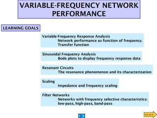
  • 1. Variable-Frequency Response Analysis Network performance as function of frequency. Transfer function Sinusoidal Frequency Analysis Bode plots to display frequency response data Resonant Circuits The resonance phenomenon and its characterization Scaling Impedance and frequency scaling Filter Networks Networks with frequency selective characteristics: low-pass, high-pass, band-pass VARIABLE-FREQUENCY NETWORK PERFORMANCE LEARNING GOALS
  • 2. °∠== 0RRZRResistor VARIABLE FREQUENCY-RESPONSE ANALYSIS In AC steady state analysis the frequency is assumed constant (e.g., 60Hz). Here we consider the frequency as a variable and examine how the performance varies with the frequency. Variation in impedance of basic components
  • 5. Frequency dependent behavior of series RLC network Cj RCjLCj Cj LjRZeq ω ωω ω ω 1)(1 2 ++ =++= C LCjRC j j ω ωω )1( 2 −+ = − − × C LCRC Zeq ω ωω 222 )1()( || −+ =       − =∠ − RC LC Zeq ω ω 1 tan 2 1 sC sRCLCs sZ sj eq 1 )( 2 ++ = ≈ωnotation"intionSimplifica"
  • 6. For all cases seen, and all cases to be studied, the impedance is of the form 01 1 1 01 1 1 ... ... )( bsbsbsb asasasa sZ n n n n m m m m ++++ ++++ = − − − − sC ZsLsZRsZ CLR 1 ,)(,)( === Simplified notation for basic components Moreover, if the circuit elements (L,R,C, dependent sources) are real then the expression for any voltage or current will also be a rational function in s LEARNING EXAMPLE sL sC 1 R So V sCsLR R sV /1 )( ++ = SV sRCLCs sRC 12 ++ = So V RCjLCj RCj V js 1)( 2 ++ = ≈ ωω ω ω °∠ +××+×× ×× = −− − 010 1)1053.215()1053.21.0()( )1053.215( 332 3 ωω ω jj j Vo MATLAB can be effectively used to compute frequency response characteristics
  • 7. USING MATLAB TO COMPUTE MAGNITUDE AND PHASE INFORMATION 01 1 1 01 1 1 ... ... )( bsbsbsb asasasa sV n n n n m m m m o ++++ ++++ = − − − − ),( ];,,...,,[ ];,,...,,[ 011 011 dennumfreqs bbbbden aaaanum nn mm >> =>> =>> − − MATLAB commands required to display magnitude and phase as function of frequency NOTE: Instead of comma (,) one can use space to separate numbers in the array 1)1053.215()1053.21.0()( )1053.215( 332 3 +××+×× ×× = −− − ωω ω jj j Vo EXAMPLE » num=[15*2.53*1e-3,0]; » den=[0.1*2.53*1e-3,15*2.53*1e-3,1]; » freqs(num,den) 1a 2b 1b 0b Missing coefficients must be entered as zeros » num=[15*2.53*1e-3 0]; » den=[0.1*2.53*1e-3 15*2.53*1e-3 1]; » freqs(num,den) This sequence will also work. Must be careful not to insert blanks elsewhere
  • 8. GRAPHIC OUTPUT PRODUCED BY MATLAB Log-log plot Semi-log plot
  • 9. LEARNING EXAMPLE A possible stereo amplifier Desired frequency characteristic (flat between 50Hz and 15KHz) Postulated amplifier Log frequency scale
  • 10. Frequency domain equivalent circuit Frequency Analysis of Amplifier )( )( )( )( sV sV sV sV in o S in = )( /1 )( sV sCR R sV S inin in in + = ]1000[ /1 /1 )( in oo o o V RsC sC sV + =       +      + = ooinin inin RsCRsC RsC sG 1 1 ]1000[ 1 )(       +    + = π π π 000,40 000,40 ]1000[ 100 ss s ( ) ( ) ( ) ( ) π π 000,401001058.79 100101018.3 191 1691 ≈××= ≈××= −−− −−− oo inin RC RC required actual π π ππ 000,40 000,40 ]1000[)(000,40||100 s s sGs ≈⇒<<<< Frequency dependent behavior is caused by reactive elements )( )( )( sV sV sG S o = Voltage Gain )50( Hz )20( kHz
  • 11. NETWORK FUNCTIONS INPUT OUTPUT TRANSFER FUNCTION SYMBOL Voltage Voltage Voltage Gain Gv(s) Current Voltage Transimpedance Z(s) Current Current Current Gain Gi(s) Voltage Current Transadmittance Y(s) When voltages and currents are defined at different terminal pairs we define the ratios as Transfer Functions If voltage and current are defined at the same terminals we define Driving Point Impedance/Admittance Some nomenclature EXAMPLE    = admittanceTransfer tanceTransadmit )( )( )( 1 2 sV sI sYT gainVoltage )( )( )( 1 2 sV sV sGv = To compute the transfer functions one must solve the circuit. Any valid technique is acceptable
  • 12. LEARNING EXAMPLE    = admittanceTransfer tanceTransadmit )( )( )( 1 2 sV sI sYT gainVoltage )( )( )( 1 2 sV sV sGv = The textbook uses mesh analysis. We will use Thevenin’s theorem sLR sC sZTH || 1 )( 1+= 1 11 RsL sLR sC + += )( )( 1 11 2 RsLsC RsLLCRs sZTH + ++ = )()( 1 1 sV RsL sL sVOC + = − + )(sVOC )(sZTH − + )(2 sV 2R )(2 sI = + = )( )( )( 2 2 sZR sV sI TH OC )( )( 1 11 2 2 1 1 RsLsC RsLLCRs R sV RsL sL + ++ + + 12121 2 2 )()( )( RCRRLsLCRRs LCs sYT ++++ = )( )( )( )( )( )( 2 1 22 1 sYR sV sIR sV sV sG T s v === )( )( 1 1 RsLsC RsLsC + + ×
  • 13. POLES AND ZEROS (More nomenclature) 01 1 1 01 1 1 ... ... )( bsbsbsb asasasa sH n n n n m m m m ++++ ++++ = − − − − Arbitrary network function Using the roots, every (monic) polynomial can be expressed as a product of first order terms ))...()(( ))...()(( )( 21 21 0 n m pspsps zszszs KsH −−− −−− = functionnetworktheofpoles functionnetworktheofzeros = = n m ppp zzz ,...,, ,...,, 21 21 The network function is uniquely determined by its poles and zeros and its value at some other value of s (to compute the gain) EXAMPLE 1)0( 22,22 ,1 21 1 = −−=+−= −= H jpjp z :poles :zeros = ++−+ + = )22)(22( )1( )( 0 jsjs s KsH 84 1 20 ++ + ss s K ⇒== 1 8 1 )0( 0KH 84 1 8)( 2 ++ + = ss s sH
  • 14. LEARNING EXTENSION Find the driving point impedance at )(sVS )( )( )( sI sV sZ S = )(sI )( 1 )()(: sI sC sIRsV in inS +=KVL =+= in in sC RsZ 1 )( Replace numerical values Ω    + M s π100 1
  • 15. LEARNING EXTENSION π)104( 000,20,50 0 7 0 21 1 ×= −=−= = K HzpHzp z :poles :zero )( )( )( sV sV sG K S o o =gainvoltagethefor ofvaluetheandlocationszeroandpoletheFind       +      + = ooinin inin RsCRsC RsC sG 1 1 ]1000[ 1 )(       +    + = π π π 000,40 000,40 ]1000[ 100 ss s For this case the gain was shown to be ))...()(( ))...()(( )( 21 21 0 n m pspsps zszszs KsH −−− −−− = Zeros = roots of numerator Poles = roots of denominator Variable Frequency Response
  • 16. SINUSOIDAL FREQUENCY ANALYSIS )(sH Circuit represented by network function    + + )cos(0 )( 0 θω θω tB eA tj ( )   ∠++ + )(cos|)(| )( 0 )( 0 ωθωω ω θω jHtjHB ejHA tj )( )()( )()( |)(|)( ωφ ωω ωωφ ωω j eMjH jH jHM = ∠= = Notation stics.characteriphaseandmagnitude calledgenerallyareoffunctionasofPlots ωωφω ),(),(M )(log )( ))(log20 10 10 ω ωφ ω PLOTSBODE vs (M    .offunctionaasfunctionnetworkthe analyzewefrequencytheoffunctionaasnetworkaofbehaviorthestudyTo ωω)( jH
  • 17. HISTORY OF THE DECIBEL Originated as a measure of relative (radio) power 1 2 )2 log10(| P P P dB =1 Pover 2 1 2 2 2 1 2 2 )2 2 2 log10log10(| I I V V P R V RIP dB ==⇒== 1 Pover By extension ||log20| ||log20| ||log20| 10 10 10 GG II VV dB dB dB = = = Using log scales the frequency characteristics of network functions have simple asymptotic behavior. The asymptotes can be used as reasonable and efficient approximations
  • 18. ]...)()(21)[1( ]...)()(21)[1()( )( 2 2 33310 bbba N jjj jjjjK jH ωτωτςωτ ωτωτςωτω ω +++ +++ = ± General form of a network function showing basic terms Frequency independent Poles/zeros at the origin First order terms Quadratic terms for complex conjugate poles/zeros ..|)()(21|log20|1|log20 ...|)()(21|log20|1|log20 ||log20log20 2 1010 2 33310110 10010 −++−+− ++++++ ±= bbba jjj jjj jNK ωτωτςωτ ωτωτςωτ ω DN D N BAAB loglog)log( loglog)log( −= += |)(|log20|)(| 10 ωω jHjH dB = 21 2 1 2121 zz z z zzzz ∠−∠=∠ ∠+∠=∠ ... )(1 2 tantan ... )(1 2 tantan 900)( 2 11 2 3 331 1 1 − − −− + − ++ °±=∠ −− −− b bb a NjH ωτ ωτς ωτ ωτ ωτς ωτ ω Display each basic term separately and add the results to obtain final answer Let’s examine each basic term
  • 19. Constant Term Poles/Zeros at the origin    °±=∠ ×±= → ± ± ± 90)( )(log20|)(| )( 10 Nj Nj j N dB N N ω ωω ω linestraightaisthis logisaxis-xthe 10ω
  • 20. Simple pole or zero ωτj+1     =+∠ +=+ − ωτωτ ωτωτ 1 2 10 tan)1( )(1log20|1| j j dB asymptotefrequencylow0|1| ≈+ dBjωτ (20dB/dec)asymptotefrequencyhighωτωτ 10log20|1| ≈+ dBj frequency)akcorner/bre1whenmeetasymptotestwoThe (=ωτ Behavior in the neighborhood of the corner FrequencyAsymptoteCurve distance to asymptote Argument corner 0dB 3dB 3 45 octave above 6dB 7db 1 63.4 octave below 0dB 1dB 1 26.6 1=ωτ 2=ωτ 5.0=ωτ °≈+∠ 0)1( ωτj °≈+∠ 90)1( ωτj ⇒<<1ωτ ⇒>>1ωτ Asymptote for phase High freq. asymptote Low freq. Asym.
  • 22. Quadratic pole or zero ])()(21[ 2 2 ωτωτς jjt ++= ])()(21[ 2 ωτωτς −+= j ( ) ( )222 102 2)(1log20|| ςωτωτ +−=dBt 2 1 2 )(1 2 tan ωτ ςωτ − =∠ − t 1<<ωτ asymptotefrequencylow0|| 2 ≈dBt °≈∠ 02t 1>>ωτ asymptotefreq.high2 102 )(log20|| ωτ≈dBt °≈∠ 1802t 1=ωτ )2(log20|| 102 ς=dBt °=∠ 902tCorner/break frequency 2 21 ςωτ −= 2 102 12log20|| ςς −=dBt ς ς 2 1 2 21 tan − =∠ − t 2 2 ≤ςResonance frequency Magnitude for quadratic pole Phase for quadratic pole dB/dec40 These graphs are inverted for a zero
  • 23. LEARNING EXAMPLE Generate magnitude and phase plots )102.0)(1( )11.0(10 )( ++ + = ωω ω ω jj j jGvDraw asymptotes for each term 1,10,50:nersBreaks/cor 40 20 0 20− dB °−90 °90 1.0 1 10 100 1000 dB|10 decdB /20− dec/45°− decdB /20 dec/45° Draw composites
  • 25. LEARNING EXAMPLE Generate magnitude and phase plots )11.0()( )1(25 )( 2 + + = ωω ω ω jj j jGv 101,:(corners)Breaks 40 20 0 20− dB °−90 °−270 °90 1.0 1 10 100 Draw asymptotes for each dB28 decdB /40− °−180 dec/45° °− 45 Form composites
  • 26. ( )2 1 02 0 0 )( K j K dB =⇔= ω ω Final results . . . And an extra hint on poles at the origin dec dB 40− dec dB 20− dec dB 40−
  • 27. LEARNING EXTENSION Sketch the magnitude characteristic )100)(10( )2(10 )( 4 ++ + = ωω ω ω jj j jG formstandardinNOTisfunctiontheBut 10010,2,:breaks Put in standard form )1100/)(110/( )12/(20 )( ++ + = ωω ω ω jj j jG We need to show about 4 decades 40 20 0 20− dB °−90 °90 1 10 100 1000 dB|25
  • 28. LEARNING EXTENSION Sketch the magnitude characteristic 2 )( 102.0(100 )( ω ω ω j j jG + = origintheatpoleDouble 50atbreak formstandardinisIt 40 20 0 20− dB °−90 °−270 °90 1 10 100 1000 Once each term is drawn we form the composites
  • 29. Put in standard form )110/)(1( )( ++ = ωω ω ω jj j jG LEARNING EXTENSION Sketch the magnitude characteristic )10)(1( 10 )( ++ = ωω ω ω jj j jG 101,:breaks origintheatzero formstandardinnot 40 20 0 20− dB °−90 °−270 °90 1.0 1 10 100 Once each term is drawn we form the composites decdB /20 decdB /20−
  • 30. LEARNING EXAMPLE A function with complex conjugate poles [ ]1004)()5.0( 25 )( 2 +++ = ωωω ω ω jjj j jG Put in standard form [ ]125/)10/()15.0/( 5.0 )( 2 +++ = ωωω ω ω jjj j jG 40 20 0 20− dB °−90 °90 01.0 1.0 1 10 100 °−270 1=ωτ )2(log20|| 102 ς−=dBt 2.0 1.0 25/12 =⇒    = = ς τ ςτ ])()(21[ 2 2 ωτωτς jjt ++= dB8 Draw composite asymptote Behavior close to corner of conjugate pole/zero is too dependent on damping ratio. Computer evaluation is better
  • 31. Evaluation of frequency response using MATLAB [ ]1004)()5.0( 25 )( 2 +++ = ωωω ω ω jjj j jG » num=[25,0]; %define numerator polynomial » den=conv([1,0.5],[1,4,100]) %use CONV for polynomial multiplication den = 1.0000 4.5000 102.0000 50.0000 » freqs(num,den) Using default options
  • 32. Evaluation of frequency response using MATLAB User controlled >> clear all; close all %clear workspace and close any open figure >> figure(1) %open one figure window (not STRICTLY necessary) >> w=logspace(-1,3,200);%define x-axis, [10^{-1} - 10^3], 200pts total [ ]1004)()5.0( 25 )( 2 +++ = ωωω ω ω jjj j jG >> G=25*j*w./((j*w+0.5).*((j*w).^2+4*j*w+100)); %compute transfer function >> subplot(211) %divide figure in two. This is top part >> semilogx(w,20*log10(abs(G))); %put magnitude here >> grid %put a grid and give proper title and labels >> ylabel('|G(jomega)|(dB)'), title('Bode Plot: Magnitude response')
  • 33. >> semilogx(w,unwrap(angle(G)*180/pi)) %unwrap avoids jumps from +180 to -180 >> grid, ylabel('Angle H(jomega)(circ)'), xlabel('omega (rad/s)') >> title('Bode Plot: Phase Response') Evaluation of frequency response using MATLAB User controlled Continued Repeat for phase No xlabel here to avoid clutter USE TO ZOOM IN A SPECIFIC REGION OF INTEREST Compare with default!
  • 34. LEARNING EXTENSION Sketch the magnitude characteristic ]136/)12/[( )1(2.0 )( 2 ++ + = ωωω ω ω jjj j jG 6/136/12 12/1 =⇒= = ςςτ τ ])()(21[ 2 2 ωτωτς jjt ++= 40 20 0 20− dB °−90 °−270 °90 1.0 1 10 100 1=ωτ )2(log20|| 102 ς−=dBt decdB /20− decdB /40− decdB /0 12 dB5.9=
  • 35. ]136/)12/[( )1(2.0 )( 2 ++ + = ωωω ω ω jjj j jG » num=0.2*[1,1]; » den=conv([1,0],[1/144,1/36,1]); » freqs(num,den)
  • 36. DETERMINING THE TRANSFER FUNCTION FROM THE BODE PLOT This is the inverse problem of determining frequency characteristics. We will use only the composite asymptotes plot of the magnitude to postulate a transfer function. The slopes will provide information on the order A A. different from 0dB. There is a constant Ko B B. Simple pole at 0.1 1 )11.0/( − +ωj C C. Simple zero at 0.5 )15.0/( +ωj D D. Simple pole at 3 1 )13/( − +ωj E E. Simple pole at 20 1 )120/( − +ωj )120/)(13/)(11.0/( )15.0/(10 )( +++ + = ωωω ω ω jjj j jG 20 | 00 0 1020| dBK dB KK =⇒= f the slope is -40dB we assume double real pole. Unless we are given more data
  • 37. LEARNING EXTENSION Determine a transfer function from the composite magnitude asymptotes plot A A. Pole at the origin. Crosses 0dB line at 5 ωj 5 B B. Zero at 5 C C. Pole at 20 D D. Zero at 50 E E. Pole at 100 )1100/)(120/( )150/)(15/(5 )( ++ ++ = ωωω ωω ω jjj jj jG Sinusoidal
  • 38. SONANT CIRCUITS - SERIES RESONANCE Im{ } 0Z⇒ = ⇒ RESONANT FREQUENCY PHASOR DIAGRAM QUALITY FACTOR
  • 39. RESONANT CIRCUITS These are circuits with very special frequency characteristics… And resonance is a very important physical phenomenon Cj LjRjZ ω ωω 1 )( ++= circuitRLCSeries Lj CjGjY ω ωω 1 )( ++= circuitRLCParallel LCC L 11 0 =⇒= ω ω ω whenzeroiscircuiteachofreactanceThe The frequency at which the circuit becomes purely resistive is called the resonance frequency
  • 40. Properties of resonant circuits At resonance the impedance/admittance is minimal Current through the serial circuit/ voltage across the parallel circuit can become very large (if resistance is small) CRR L Q 0 0 1 ω ω ==:FactorQuality 222 ) 1 (|| 1 )( C LRZ Cj LjRjZ ω ω ω ωω −+= ++= 222 ) 1 (|| 1 )( L CGY Cj Lj GjY ω ω ω ω ω −+= ++= Given the similarities between series and parallel resonant circuits, we will focus on serial circuits
  • 41. Properties of resonant circuits At resonance the power factor is unity CIRCUIT BELOW RESONANCE ABOVE RESONANCE SERIES CAPACITIVE INDUCTIVE PARALLEL INDUCTIVE CAPACITIVE Phasor diagram for series circuit Phasor diagram for parallel circuit − + RV − −= + C I jVC ω − + Ljω 1GV 1CVjω L V j ω 1 −
  • 42. LEARNING EXAMPLE Determine the resonant frequency, the voltage across each element at resonance and the value of the quality factor LC 1 0 =ω sec/2000 )1010)(1025( 1 63 rad FH = ×× = −− I A Z V I S 5 2 010 = °∠ == Ω= 2ZresonanceAt Ω=××= − 50)1025)(102( 33 0Lω )(902505500 VjLIjVL °∠=×== ω °−∠=×−== Ω== 90250550 1 50 1 0 0 0 jI Cj V L C C ω ω ω R L Q 0ω = 25 2 50 == |||| |||| 0 SC S S L VQV VQ R V LV = ==ω resonanceAt
  • 43. LEARNING EXAMPLE Given L = 0.02H with a Q factor of 200, determine the capacitor necessary to form a circuit resonant at 1000Hz R L0 200 ω =⇒= 200QwithL LC 1 0 =ω C02.0 1 10002 =×⇒ π FC µ27.1=⇒ What is the rating for the capacitor if the circuit is tested with a 10V supply? VVC 2000|| =⇒|||| |||| 0 SC S S L VQV VQ R V LV = ==ω resonanceAt Ω= ×× =⇒ 59.1 200 02.010002π R AI 28.6 59.1 10 == The reactive power on the capacitor exceeds 12kVA
  • 44. LEARNING EXTENSION Find the value of C that will place the circuit in resonance at 1800rad/sec LC 1 0 =ω 2 18001.0 1 )(1.0 1 1800 × =⇒ × = C CH FC µ86.3= Find the Q for the network and the magnitude of the voltage across the capacitor R L Q 0ω = 60 3 1.01800 = × =Q |||| |||| 0 SC S S L VQV VQ R V LV = ==ω resonanceAt VVC 600|| =
  • 45. Resonance for the series circuit 222 ) 1 (|| 1 )( C LRZ Cj LjRjZ ω ω ω ωω −+= ++= QR CQRL 1 , 00 == ωω :resonanceAt       −+= −+= )(1 )( 0 0 0 0 ω ω ω ω ω ω ω ω ω jQR QRjQRjRjZ )(1 1 0 0 1 ω ω ω ω −+ == jQV V G R v isgainvoltageThe:Claim )(1 ω ω ω jZ R Cj LjR R Gv = ++ = vv GGM ∠== |)(|,|)( ωφω 2/1 20 0 2 )(1 1 )(       −+ = ω ω ω ω ω Q M )(tan)( 0 0 1 ω ω ω ω ωφ −−= − Q Q BW 0ω =         +      +−= 1 2 1 2 1 2 0 QQ LO ωω sfrequenciepowerHalf Z R Gv =
  • 46. The Q factor CRR L Q 0 0 1 ω ω == RLowQHigh:circuitseriesFor ⇔ G)(lowRHighQHigh:circuitparallelFor ⇔ M BWSmallQHigh ⇔ dissipates Stores as E field Stores as M field Capacitor and inductor exchange stored energy. When one is at maximum the other is at zero D S W W Q π2= cyclebydissipatedenergy storedenergymaximum π2= Q can also be interpreted from an energy point of view π ω π ω 22 1 2 0202 ×=×= mxeffD RIRIW 22 2 1 2 1 mxmxS CVLIW == ππ ω 22 0 Q R L W W D s = × =
  • 47. ERGY TRANSFER IN RESONANT CIRCUITS Normalization factor ( ) cos [ ]m O V i t t A R ω=
  • 48. LEARNING EXAMPLE Ω2 mH2 Fµ5 Determine the resonant frequency, quality factor and bandwidth when R=2 and when R=0.2 CRR L Q 0 0 1 ω ω == LC 1 0 =ω Q BW 0ω = sec/10 )105)(102( 1 4 630 rad= ×× = −− ω R Q 2 10 0.2 100 R Q BW(rad/sec) 2 10 1000 0.2 100 100 Evaluated with EXCEL R Q 002.010000× = QBW /10000=
  • 49. LEARNING EXTENSION A series RLC circuit as the following properties: sec/100sec,/4000,4 0 radBWradR ==Ω= ω Determine the values of L,C. CRR L Q 0 0 1 ω ω == LC 1 0 =ω Q BW 0ω = 1. Given resonant frequency and bandwidth determine Q. 2. Given R, resonant frequency and Q determine L, C. 40 100 40000 === BW Q ω H QR L 040.0 4000 440 0 = × == ω F RQL C 6 62 0 2 0 1056.1 1016104 111 − − ×= ××× === ωω
  • 50. LEARNING EXAMPLE Find R, L, C so that the circuit operates as a band-pass filter with center frequency of 1000rad/s and bandwidth of 100rad/s )(1 ω ω ω jZ R Cj LjR R Gv = ++ = CRR L Q 0 0 1 ω ω == LC 1 0 =ω Q BW 0ω = dependent Strategy: 1. Determine Q 2. Use value of resonant frequency and Q to set up two equations in the three unknowns 3. Assign a value to one of the unknowns 10 100 10000 === BW Q ω R L R L Q 1000 100 =⇒= ω LCLC 1 )10( 1 23 0 =⇒=ω For example FFC 6 101 − == µ HL 1= Ω=100R
  • 51. PROPERTIES OF RESONANT CIRCUITS: VOLTAGE ACROSS CAPACITOR |||| 0 RVQV = resonanceAt But this is NOT the maximum value for the voltage across the capacitor CRjLC Cj LjR Cj V V S ωω ω ω ω +− = ++ = 2 0 1 1 1 1 ( )               +− = 2 22 1 1 )( Q u u ug 2 0 0 ; SV V gu == ω ω ( ) 22 22 2 1 )/1)(/(2)2)(1(2 0               +− +−− == Q u u QQuuu du dg CRR L Q 0 0 1 ω ω == LC 1 0 =ω 2 2 1 )1(2 Q u =−⇒ 2 0 max max 2 1 1 Q u −== ω ω 2 2 424 max 4 1 1 2 11 4 1 1 Q Q QQQ g − =       −+ = 2 0 4 1 1 || || Q VQ V S − =
  • 52. LEARNING EXAMPLE mH50 Fµ5 Ω=Ω= 150, RR andwhenDetermine max0 ωω Natural frequency depends only on L, C. Resonant frequency depends on Q. srad LC /2000 )105)(105( 11 620 = ×× == −− ω CRR L Q 0 0 1 ω ω == LC 1 0 =ω 2 0 max max 2 1 1 Q u −== ω ω R Q 050.02000× = 2max 2 112000 Q −×=ω R Q Wmax 50 2 1871 1 100 2000 Evaluated with EXCEL and rounded to zero decimals Using MATLAB one can display the frequency response
  • 54. LEARNING EXAMPLE The Tacoma Narrows Bridge Opened: July 1, 1940 Collapsed: Nov 7, 1940 Likely cause: wind varying at frequency similar to bridge natural frequency 2.020 ×= πω
  • 55. Tacoma Narrows Bridge Simulator )11( ftV = 42 40 ≈ + = BA B in RR R v v resonanceatmodeltheFor .deflection4'causedwind42mphafailureAt Ω1 Ω5.9H20 Fµ66.31 42=mxVin Assume a low Q=2.39 0.44’ 1.07’ '77.3
  • 56. PARALLEL RLC RESONANT CIRCUITS 222 ) 1 (|| 1 )( C LRZ Cj LjRjZ ω ω ω ωω −+= ++= 222 ) 1 (|| 1 )( L CGY Cj Lj GjY ω ω ω ω ω −+= ++= Impedance of series RLC Admittance of parallel RLC IVYZ LCCLGR ↔↔ ↔↔↔ , ,, esequivalencNotice SS YVI = SSL SSC SSG I Y Lj V Lj I I Y Cj CVjI I Y G GVI ω ω ω ω 1 1 == == == || 1 || |||| 1 0 0 SL SC LC SG I LG I I G C I II II GY L C ω ω ω ω = = −= = =⇒= 0 0 resonanceAt CRR L Q 0 0 1 ω ω == LC 1 0 =ω Series RLC Parallel RLC LGG C Q 0 0 1 ω ω == LC 1 0 =ω || SIQ= Series RLC Q BW 0ω = Parallel RLC Q BW 0ω =
  • 57. VARIATION OF IMPEDANCE AND PHASOR DIAGRAM – PARALLEL CIRCUIT
  • 58. LEARNING EXAMPLE mHLFC SGVS 120,600 01.0,0120 == =°∠= µ If the source operates at the resonant frequency of the network, compute all the branch currents SSL SSC SSG I Y Lj V Lj I I Y Cj CVjI I Y G GVI ω ω ω ω 1 1 == == == || 1 || |||| 1 0 0 SL SC LC SG I LG I I G C I II II GY L C ω ω ω ω = = −= = =⇒= 0 0 resonanceAt || SIQ= SG IAI =°∠=°∠×= )(02.1012001.0 srad LC /85.117 )106(120.0 11 40 = ×× == − ω )(9049.80120)10600()85.117()901( 6 AIC °∠=°∠××××°∠= − )(9049.8 AIL °−∠= _______=xI
  • 59. LEARNING EXAMPLE Derive expressions for the resonant frequency, half power frequencies, bandwidth and quality factor for the transfer characteristic in out I V H = Lj CjGYT ω ω 1 ++= Tin out T in out YI V H Y I V 1 ==⇒= 2 2 1 1 1 1 ||       −+ = ++ = L CGLj CjG H ω ωω ω LC 1 0 =ω:frequencyResonant 22 max ||5.0|)(| HjH h =⇒ ωsfrequenciepowerHalf 2 2 2 2 1 G L CG h h =      −+ ω ω R G H == 1 || max G L C h h ±=−⇒ ω ω 1 LCC G C G h 1 22 2 +      += ω C G BW LOHI =−= ωω L C R L C GBW Q === 10ω LGG C Q 0 0 1 ω ω ==         +      +−= 1 2 1 2 1 2 0 QQ LO ωω Replace and show
  • 60. LEARNING EXAMPLE Increasing selectivity by cascading low Q circuits Single stage tuned amplifier ( )( ) MHzsrad FHLC 9.99/10275.6 1054.210 11 8 1260 =×= × == −− ω 398.0 10 1054.2 250 6 12 = × ×= − − L C R L C GBW Q === 10ω
  • 61. LEARNING EXTENSION Determine the resonant frequency, Q factor and bandwidth FCmHLkR µ150,20,2 ==Ω= Parallel RLC LGG C Q 0 0 1 ω ω == LC 1 0 =ω Q BW 0ω = srad /577 )10150)(1020( 1 630 = ×× = −− ω ( ) 173 2000/1 10150577 6 = ×× = − Q sradBW /33.3 173 577 ==
  • 62. LEARNING EXTENSION 0C,L,Determine ω 120,/1000,6 ==Ω= QsradBWkR Parallel RLC LGG C Q 0 0 1 ω ω == LC 1 0 =ω Q BW 0ω = sradBWQ /102.11000120 5 0 ×=×=×=ω F R Q C µ ω 167.0 102.16000 120 5 0 = ×× == H Q R L µ ω 417 102.1120 6000 5 0 = ×× == Can be used to verify computations
  • 63. PRACTICAL RESONANT CIRCUIT The resistance of the inductor coils cannot be neglected LjR CjjY ω ωω + += 1 )( LjR LjR ω ω − − × 22 )( )( LR LjR CjjY ω ω ωω + − +=       + −+ + = 2222 )()( )( LR L Cj LR R jY ω ω ω ω 2 22 1 0 )(       −=⇒= + −⇒ L R LCLR L CY Rω ω ω real ⇒== R L Q LC 0 00 , 1 ω ω 2 0 0 1 1 Q R −=ωω maximaareimpedanceandvoltagetheresonanceAt. Y I ZIV == ( )                     +=               += + = 2 0 2 0 222 11 R L R R L R R LR Z RRR MAX ω ω ωωω 2 0RQZMAX = How do you define a quality factor for this circuit?
  • 64. LEARNING EXAMPLE ΩΩ= 5,50, RR forbothDetermine 0 ωω ⇒== R L Q LC 0 00 , 1 ω ω 2 0 0 1 1 Q R −=ωω srad FH /2000 )105)(1050( 1 630 = ×× = −− ω 2 0 0 1 12000, 050.02000 QR Q R −= × = ω R Q0 Wr(rad/s) f(Hz) 50 2 1732 275.7 5 20 1997 317.8
  • 65. RESONANCE IN A MORE GENERAL VIEW 222 ) 1 (|| 1 )( C LRZ Cj LjRjZ ω ω ω ωω −+= ++= 222 ) 1 (|| 1 )( L CGY Cj Lj GjY ω ω ω ω ω −+= ++= For series connection the impedance reaches maximum at resonance. For parallel connection the impedance reaches maximum 1)(1)( 22 ++ = ++ = LGjLCj Lj Z CRjLCj Cj Y ps ωω ω ωω ω 12)( 2 ++ ωτςωτ jj aswrittenwastermquadratictheplotsBodeIn 0 1 ω τ == LC Q CRCR 1 22 0 ==⇒= ωςςτ series Q LGLG 1 22 0 ==⇒= ωςςτ parallel ς2 1 =QA high Q circuit is highly under damped Resonance
  • 66. SCALING Scaling techniques are used to change an idealized network into a more realistic one or to adjust the values of the components M M M K C C LKL RKR → → → ' ' ' scalingimpedanceorMagnitude '' 11 '' 0 CLLC CLLC ==⇒= ω ' '00 R L R L Q ωω == Magnitude scaling does not change the frequency characteristics nor the quality of the network. CC LL ωKω' F ωω ωω 1 '' 1 ,'' == → unchangediscomponenteachofImpedance scalingtimeorFrequency F F K C C K L L RR → → → ' ' ' 0 ' 0 ωω FK= )( ' ' ' 0 BWK Q BW F== ω Q R L Q == ' ' ' ' 0ω Constant Q networks
  • 67. LEARNING EXAMPLE Ω= 2 H1= F 2 1 Determine the value of the elements and the characterisitcs of the network if the circuit is magnitude scaled by 100 and frequency scaled by 1,000,000 2, 2 2 ,/20 === BWQsradω FC HL R 200 1 ' 100' 200' = = Ω= M M M K C C LKL RKR → → → ' ' ' scalingimpedanceorMagnitude F F K C C K L L RR → → → ' ' ' FC mHL R µ 200 1 '' 100'' 200'' = = Ω= 0 ' 0 ωω FK= )( ' ' ' 0 BWK Q BW F== ω srad /10414.1 6'' 0 ×=ω unchangedare0,ωQ
  • 69. FILTER NETWORKS Networks designed to have frequency selective behavior COMMON FILTERS Low-pass filter High-pass filter Band-pass filter Band-reject filter We focus first on PASSIVE filters
  • 70. Simple low-pass filter RCj Cj R Cj V V Gv ω ω ω + = + == 1 1 1 1 1 0 RC j Gv = + = τ ωτ ; 1 1 ( ) ωτωφ ωτ ω 1 2 tan)( 1 1 ||)( − −==∠ + == v v G GM 2 11 ,1max =      == τ ωMM frequencypowerhalf== τ ω 1 τ 1 =BW
  • 71. Simple high-pass filter CRj CRj Cj R R V V Gv ω ω ω + = + == 111 0 RC j j Gv = + = τ ωτ ωτ ; 1 ( ) ωτ π ωφ ωτ ωτ ω 1 2 tan 2 )( 1 ||)( − −==∠ + == v v G GM 2 11 ,1max =      == τ ωMM frequencypowerhalf== τ ω 1 τ ω 1 =LO
  • 72. Simple band-pass filter Band-pass       −+ == C LjR R V V Gv ω ω 11 0 ( ) ( )222 1 )( −+ = LCRC RC M ωω ω ω 1 1 =      = LC M ω 0)()0( =∞=== ωω MM ( ) 2 4/)/( 2 0 2 ω ω ++− = LRLR LO LC 1 0 =ω ( ) 2 4/)/( 2 0 2 ω ω ++ = LRLR HI L R BW LOHI =−= ωω )( 2 1 )( HILO MM ωω ==
  • 73. Simple band-reject filter 0 11 0 00 =      −⇒= C Lj LC ω ωω 10 VV =⇒= circuitopenasactscapacitorthe0at ω 10 VV =⇒∞= circuitopenasactsinductortheat ω filterpass-band theinasdeterminedareHILO ωω ,
  • 74. LEARNING EXAMPLE Depending on where the output is taken, this circuit can produce low-pass, high-pass or band-pass or band- reject filters Band-pass Band-reject filter       −+ = C LjR Lj V V S L ω ω ω 1 ( ) 1)(,00 =∞=== ωω S L S L V V V V High-pass       −+ = C LjR Cj V V S C ω ω ω 1 1 ( ) 0)(,10 =∞=== ωω S C S C V V V V Low-pass FCHLR µµ 159,159,10 ==Ω=forplotBode
  • 75. LEARNING EXAMPLE A simple notch filter to eliminate 60Hz interference ) 1 ( 1 1 C Lj C L Cj Lj Cj Lj ZR ω ω ω ω ω ω − = + = in Req eq V ZR R V + =0 ∞=      = LC ZR 1 ω 0 1 0 =      =∴ LC V ω ( ) ( )tttvin 10002sin2.0602sin)( ×+×= ππ FCmHL µ100,3.70 ==
  • 76. LEARNING EXTENSION )( ωjGvforplotBodetheofsticcharacterimagnitudetheSketch RCj Cj R Cj jGv ω ω ω ω + = + = 1 1 1 1 )( sradFRC /2.0)1020)(1010( 63 =×Ω×== − τ 20dB/dec-ofasymptotefrequencyHigh 0dB/decofasymptotefrequencylow 5rad/s:frequencyerBreak/corn
  • 77. LEARNING EXTENSION )( ωjGvforplotBodetheofsticcharacterimagnitudetheSketch RCj RCj Cj R R jGv ω ω ω ω + = + = 11 )( sradFRC /5.0)1020)(1025( 63 =×Ω×== − τ srad /2 1 == τ ωat0dBCrosses20dB/dec. 20dB/dec-ofasymptotefrequencyHigh 0dB/decofasymptotefrequencylow 2rad/s:frequencyerBreak/corn
  • 78. LEARNING EXTENSION )( ωjGvforplotBodetheofsticcharacterimagnitudetheSketch Band-pass LCjRCj RCj Lj Cj R R jGv 2 )(11 )( ωω ω ω ω ω ++ = ++ = 5.0 102 10 10102 ,1010 3 3 63 362 = × =⇒×== ==⇒= − − − −− ςςτ ττ RC LC srad RC /1000 1 ==ωat0dBCrosses20dB/dec. 40dB/dec-ofasymptotefrequencyHigh 0dB/decofasymptotefrequencylow rad/s1000:frequencyerBreak/corn ( ) 2 4/)/( 2 0 2 ω ω ++− = LRLR LO ( ) 2 4/)/( 2 0 2 ω ω ++ = LRLR HI 1000 1 0 == LC ω srad /618= srad /1618= decdB /40−
  • 79. ACTIVE FILTERS Passive filters have several limitations 1. Cannot generate gains greater than one 2. Loading effect makes them difficult to interconnect 3. Use of inductance makes them difficult to handle Using operational amplifiers one can design all basic filters, and more, with only resistors and capacitors The linear models developed for operational amplifiers circuits are valid, in a more general framework, if one replaces the resistors by impedances Ideal Op-Amp These currents are zero
  • 80. Basic Inverting Amplifier 0=+V +− =⇒ VVgainInfinite 0=−V 0==⇒ +II-impedanceinputInfinite 0 2 2 1 1 =+ Z V Z V 1 1 2 2 V Z Z V −= Linear circuit equivalent 0=−I 1 2 Z Z G −= 1 1 1 Z V I =
  • 81. Basic Non-inverting amplifier 1V 1V 0=+I 1 1 2 10 Z V Z VV = − 1 1 12 0 V Z ZZ V + = 1 2 1 Z Z G += 01 =I Basic Non-inverting Amplifier Due to the internal op-amp circuitry, it has limitations, e.g., for high frequency and/or low voltage situations. The Operational Transductance Amplifier (OTA) performs well in those situations
  • 82. Operational Transductance Amplifier (OTA) ∞== 0RRin:OTAIdeal MPARISON BETWEEN OP-AMPS AND OTAs – PHYSICAL CONSTRUCTION Comparison of Op-Amp and OTA - Parameters Amplifier Type Ideal Rin Ideal Ro Ideal Gain Input Current input Voltage Op-Amp 0 0 0 OTA gm 0 nonzero ∞ ∞ ∞ ∞
  • 83. Basic Op-Amp Circuit Basic OTA Circuit       +      + == + = + = inS in v L L S S inS in in inv L L RR R A RR R V v A V RR R v vA RR R v 0 0 0 0       +      + == + = + = inS in m Lin m S inS in in inm L RR R g RR R v i G V RR R v vg RR R i 0 00 0 0 0 ∞== vAA Amp-OpIdeal mm gG = OTAIdeal
  • 84. Basic OTA Circuits )0()( 1 0 0 00 10 vdxxi C v vgi t m += = ∫ )0()()( 0 0 10 vdxxv C g tv t m += ∫ Integrator In the frequency domain 10 V Cj g V m ω = 00 0 =+ −= ii vgi in inm polarity)(notice m eq in in g R i v 1 == ResistorSimulated
  • 85. Basic OTA Adder 11vgm 22vgm 21 21 vgvg mm + ResistorSimulated Equivalent representation OTA APPLICATION )( 1 21 3 0 21 vgvg g v mm m +=
  • 87. LEARNING EXAMPLE ABCm m m Ig S mS g mSg 20 104 10 4 4 7 4 = ×=≥ ≤ − resistoraProduce Ωk25 SSg g m m 753 104104 1 1025 −− ×>×=⇒=× m eq in in g R i v 1 == ResistorSimulated )(20104 5 AI A S S ABC    =× − AAIABC µ2102 6 =×= −
  • 88. LEARNING EXAMPLE Floating simulated resistor 1101 vgi m−= 1202 vgi m= inmvgi −=0 One grounded terminal 011 ii −= 102 ii = 21 mm gg = operationproperFor ABCm m m Ig S mS g mSg 20 104 10 4 4 7 4 = ×=≥ ≤ − resistor10MaProduce Ω Sgm 7 6 10 1010 1 − = × = S7 104 − ×< The resistor cannot be produced with this OTA!
  • 89. LEARNING EXAMPLE 210 210 321 210 210 ,,, vvv vvv ggg mmm −= += b) a) producetoSelect ABCm m m Ig S mS g mSg 20 104 10 4 4 7 4 = ×=≥ ≤ − )( 1 21 3 0 21 vgvg g v mm m += Case a 2;10 3 2 3 1 == m m m m g g g g Two equations in three unknowns. Select one transductance )(10 20 1 1.0 4 33 AImSg ABCm − ×=⇒= Aµ5= AImSg ABCm µ102.0 22 =⇒= AImSg ABCm µ501 11 =⇒= Case b Reverse polarity of v2!
  • 90. ANALOG MULTIPLIER ASSUMES VG IS ZERO Based on ‘modulating the control current
  • 91. AUTOMATIC GAIN CONTROL For simplicity of analysis we drop the absolute value IN O IN IN O v small v Av A v big v B ⇒ ≈ ⇒ ≈
  • 92. OTA-C CIRCUITS Circuits created using capacitors, simulated resistors, adders and integrators integrator resistor Frequency domain analysis assuming ideal OTAs 1101 im VgI = 0202 VgI m−= 0201 IIIC +=CI Cj V ω 1 0 = [ ]02110 1 VgVg Cj V mim −= ω 1 2 2 1 0 1 i m m m V g Cj g g V ω+ = Magnitude Bode plot 1 0 i v V V G = 2 1 m m dc g g A = C g f C g m C m C 2 2 2 = = π ω
  • 93. LEARNING EXAMPLE )10(2 1 4 5 1 0 π ωjV V G i v + ==:Desired ABCm m m Ig S mS g mSg 20 10 10 1 1 6 3 = =≥ ≤ − 4=dcA kHzfCC 100)10(2 5 =⇒= πω 2 1 m m dc g g A = C g f C g m C m C 2 2 2 = = π ω Two equations in three unknowns. Select the capacitor value pFC 25= Sgm 6125 2 107.15)1025)(10(2 −− ×=×= π OK AISg ABCm µµ 14.38.62 11 =⇒= AIABC µ785.0 20 7.15 2 == biasesandncestransductatheFind
  • 94. TOW-THOMAS OTA-C BIQUAD FILTER biquad ~ biquadratic 2 0 02 2 0 )()( )()( ωω ω ω ωω ++ ++ = j Q j CjBjA V V i Cj VV gV i m ω 021 101 − = )( 201202 im VVgI −= )( 23303 oim VVgI −= )( 1 0302 2 02 II Cj V += ω 03i )(unknownsfourandequationsFour 02010201 ,,, IIVV 1)()( 12 132 21 21 3 2 3 21 2 3 2 2 01 +                  −+      + = + ωω ω j gg Cg j gg CC V g g VV g g g Cj V mm m mm i m m ii m m m 1)()( 12 132 21 21 3 21 31 2 1 1 1 02 +                  +      − = + ωω ωω j gg Cg j gg CC V gg gCj V g Cj V V mm m mm i mm m i m i 1 2 2 3 21 2 30 21 21 0 ,, C C g gg Q C g QCC gg m mmmmm === ω ω Filter Type A B C Low-pass 0 0 nonzero Band-pass 0 nonzero 0 High-pass nonzero 0 0         = = = ⇒    = = C g BW g g Q C g CC gg m m m m mm 3 3 0 21 21 ω
  • 95. LEARNING EXAMPLE ABCm m m Ig S mS g mSg 20 104 10 4 4 7 4 = ×=≥ ≤ − 5.-gainfrequencycenterand75kHz,ofbandwidth 500kHz,offrequencycenterwithfilterpass-bandaDesign 1)()( 12 132 21 21 3 21 31 2 1 1 1 02 +                  +      − = + ωω ωω j gg Cg j gg CC V gg gCj V g Cj V V mm m mm i mm m i m i 1 2 2 3 21 2 30 21 21 0 ,, C C g gg Q C g QCC gg m mmmmm === ω ω capacitorspF-50andionconfiguratThomas-TowtheUse BW 03 =iV 3 2 0 |)(| m m v g g jG =ω 0)(1 2 21 21 0 =      +⇒= ωωω j gg CC mm 21 CC = S g BW m µπ 56.2310752 1050 3 12 3 =××= × = − Sgm µ8.1175 2 =⇒= ( ) ( ) 213 6 1252 0 )105( 108.117 1052 − − × ×× =××= mg πω Sgm µ5.2091 =⇒ AI AI AI ABC ABC ABC µ µ µ 18.1 89.5 47.10 3 2 1 = = =
  • 96. Bode plots for resulting amplifier
  • 97. LEARNING BY APPLICATION Using a low-pass filter to reduce 60Hz ripple Thevenin equivalent for AC/DC converter Using a capacitor to create a low- pass filter Design criterion: place the corner frequency at least a decade lower TH TH OF V CRj V ω+ = 1 1 ( )2 1 || || CR V V TH TH OF ω+ = CRTH C 1 =ω ||1.0|| THOF VV ≈ FCC µ π 05.53 62 1 500 =⇒ × =
  • 99. LEARNING EXAMPLE Single stage tuned transistor amplifier Select the capacitor for maximum gain at 91.1MHz Antenna Voltage Transistor Parallel resonant circuit    −= Cj LjR V V A ωω 1|||| 1000 40 LCRC j j Cj V V Cj Cj Cj LjR A 1 )( / 1000 4 / / 11 1 1000 4 2 0 ++ −= × ++ −= ω ω ω ω ω ω ω LC/1frequencycenterwithpass-Band ( ) ⇒=× − C6 6 10 1 101.912π pFC 05.3= 100 1000 410 ==      = R LCV V A ω AV V0forplotBodeMagnitude
  • 100. LEARNING BY DESIGN Anti-aliasing filter Nyquist Criterion When digitizing an analog signal, such as music, any frequency components greater than half the sampling rate will be distorted In fact they may appear as spurious components. The phenomenon is known as aliasing. SOLUTION: Filter the signal before digitizing, and remove all components higher than half the sampling rate. Such a filter is an anti-aliasing filter For CD recording the industry standard is to sample at 44.1kHz. An anti-aliasing filter will be a low-pass with cutoff frequency of 22.05kHz Single-pole low-pass filter RCjV V in ω+ = 1 101 050,222 1 ×== πω RC C Ω=⇒= kRnFC 18.721 Resulting magnitude Bode plot Attenuation in audio range
  • 101. Improved anti-aliasing filter Two-stage buffered filter − + 01v RCjV V ω+ = 1 1 01 02 RCjV V in ω+ = 1 101 One-stage Two-stage Four-stage ( )n in n RCjV V ω+ = 1 10 stage-n
  • 102. mHL FC 704.0 10 = = µ Magnitude Bode plot ( )sCsLRR R V V tapeamp amp tape amp /1||++ =               +        + + + + = 1 1 2 2 tapeamp tapeamp amp tape amp RR L sLCs LCs RR R V V LC 1 =frequencynotch To design, pick one, e.g., C and determine the other LEARNING BY DESIGN Notch filter to eliminate 60Hz hum Notch filter characteristic
  • 103. DESIGN EXAMPLE ANTI ALIASING FILTER FOR MIXED MODE CIRCUITS Visualization of aliasing Signals of different frequency and the same samples Ideally one wants to eliminate frequency components higher than twice the sampling frequency and make sure that all useful frequencies as properly sampled Design specification Simplifying assumption Infinite input resistance (no load on RC circuit) Design equation 15.9R k∴ = Ω
  • 104. (non-inverting op-amp) DESIGN EXAMPLE“BASS-BOOST” AMPLIFIER DESIRED BODE PLOT OPEN SWITCH (6dB) 500 2P f = Switch closed??
  • 105. DESIGN EXAMPLE TREBLE BOOST Original player response Desired boost Proposed boost circuit Non-inverting amplifier Design equations Filters