
Recommended
More Related Content
What's hot
What's hot (20)
Viewers also liked
Viewers also liked (18)
Similar to Patent Technology Evaluation Report
Similar to Patent Technology Evaluation Report (20)
Recently uploaded
Recently uploaded (20)
Patent Technology Evaluation Report
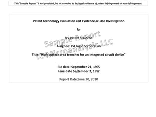
- 1. This “Sample Report” is not provided for, or intended to be, legal evidence of patent infringement or non-infringement. Patent Technology Evaluation and Evidence-of-Use Investigation for US Patent 5662768 Assignee: LSI Logic Corporation Title: “High surface area trenches for an integrated circuit device” File date: September 21, 1995 Issue date September 2, 1997 Report Date: June 20, 2010
- 2. This “Sample Report” is not provided for, or intended to be, legal evidence of patent infringement or non-infringement. Table of Contents Page # Patent Technology Evaluation and Evidence-of-Use Investigation 1 Table of Contents and Figures 2-3 Introduction/Objective 4 Summary of Final Results 4-7 Patent Technology Evaluation 8 - 17 Introduction/Objective Summary of Results 9 Discussion 10 - 17 Evidence of Use Study - Part 1: Focused Citation Analysis 18 - 24 Introduction/Objective 19 Summary of Results 20 Discussion 21 - 24 Evidence of Use Study - Part 2: Technology Claim Diagrams 25 - 168 Introduction/Objective 26 Summary of Results 26 Discussion 27 - 168 Evidence-of-Use Study - Part 3: Patent Technology Utilization Research and Analysis 169 - 188 Introduction/Objective 170 - 171 Summary of Results 172 - 175 Discussion 176 - 188 References and Patent Links 189 - 191 2 IC Microanalysis, LLC - www.icmicroanalysis.com - Email: icmicroanalysis@cox.net - Phone: 602-828-2606
- 3. This “Sample Report” is not provided for, or intended to be, legal evidence of patent infringement or non-infringement. List of Figures Figures # Preferred Embodiments of Invention 1 Second Embodiment of Invention 2 Third Embodiment of Invention 3 Independent Claims Analysis – Claims 1, 15, 20 4 Independent Claims Analysis – Claims 24, 27, 33 5 Patent Groups reviewed and analyzed 6 Final Working Group Assignees 7 Table illustrating the top Groups 1 - 3 References 8 Chart illustrating the top Groups 1 - 3 References 9 Chart illustrating the top Groups 1 - 2 References 10 Technology Claim Diagrams 11 - 151 IC Microanalysis, LLC - www.icmicroanalysis.com - Email: icmicroanalysis@cox.net - Phone: 602-828-2606 3
- 4. This “Sample Report” is not provided for, or intended to be, legal evidence of patent infringement or non-infringement. Introduction/Objective A Patent Technology Evaluation and Evidence-of-Use Investigation was performed on US Patent 5662768 titled “High surface area trenches for an integrated circuit device” (1) The patent had a filing date of September 21, 1995 and an issue date of September 2, 1997. The assignee was identified as LSI Logic Corporation. The objective of this project was to extract and evaluate the technical elements of the invention, attempt to determine which manufacturers and/or products might incorporate aspects of the invention, and provide documentation of the similarities. Results and conclusions are not a legal opinion. Summary of Final Results • US Patent 5662768 (‘768) describes a process for forming trenches having “high surface-area sidewalls with undulating profiles”. (1) • Claims 1 and 20 are the broadest claims. • Embodiments are included for both general trench structures (such as isolation) and trench memory capacitors. • Ten different Assignees were found to have patents on structures and/or processes that appeared to have multiple similar elements to claims of the ‘768 claims. These include Chartered Semiconductor,, Infineon Technologies AG, International Business Machines Corp, Kabushiki Kaisha Toshiba, Micron Semiconductor, Nanya Technology Corporation, Samsung Electronics, Taiwan Semiconductor Manufacturing Company, United Microelectronics Corp., and Vanguard Semiconductor. Some of these cited the ‘768 as prior art. • Diagrams and text descriptions of current products from some of the Final Working Group patent Assignees appeared to show similarities to multiple elements of the ‘768 patent claims. Detailed cross-section images of actual parts and description of trench manufacturing processes may be required to compare claim elements to real-world product features. IC Microanalysis, LLC - www.icmicroanalysis.com - Email: icmicroanalysis@cox.net - Phone: 602-828-2606 4
- 5. This “Sample Report” is not provided for, or intended to be, legal evidence of patent infringement or non-infringement. LAM Research, Applied Materials, or Silicon Genesis Although their equipment is used by other manufacturers to fabricate a variety of semiconductor products, neither LAM Research, Applied Materials, or Silicon Genesis fabricates their own trench or stacked DRAMs so no further research was performed on these Assignees. Chartered Semiconductor Chartered Semiconductor is now a part of GlobalFoundries, who do not appear to currently utilize trench eDRAMs modules or any other trench-based memory technology. Chartered Semiconductor Chartered Semiconductor is now part of GlobalFoundries, who do not appear to currently utilize trench eDRAMs modules or any other trench-based memory technology. Infineon Infineon uses a deep trench capacitor-based DRAM cell with a “bottle-shaped” trench and hemispherical silicon grains (HSG) to extend the effective surface area. This may be similar to the elements of Claim 20 and others. International Business Machines Corp. IBM currently integrates a “bottle-shaped” embedded DRAM capacitor in their SOI-based processes. This may be similar to the elements of Claims 1, 20 and others. IC Microanalysis, LLC - www.icmicroanalysis.com - Email: icmicroanalysis@cox.net - Phone: 602-828-2606 5
- 6. This “Sample Report” is not provided for, or intended to be, legal evidence of patent infringement or non-infringement. Kabushiki Kaisha Toshiba Toshiba currently manufacturers a “bottle-shaped” trench capacitor embedded DRAM memory cell. This may have similarities to Claims 1, 20 and others. Micron Technology Micron Semiconductor currently manufacturers only stacked capacitor DRAM memories. Nanya Technology Corporation Nanya has used Qimonda trench (bottle-shaped) capacitor DRAM technology in the past , but is converting its capacity over to Micron Technology Inc. stacked-capacitor DRAM technology. The Qimonda devices may have similarities to Claim 20 and others. Inotera Memories Nanya and Micron Technology have a “Joint Technology Development Agreement” called Inotera Memories Inc. which currently has a deep trench capacitor DRAM (at 90nm – 75nm) but is converting to stacked- capacitor DRAM technologies at 50nm. Samsung Electronics Co., Ltd Samsung currently utilizes Metal-Insulator-Metal (MIM) capacitor technology for DRAM cells. However, their Sphere-shaped Recess Channel Array Transistor (S-RACT) has some elements similar to Claim 20 of the ‘768 patent. Trench cross -section images of actual products would help determine if elements of Claims 1 and 20 are similar. IC Microanalysis, LLC - www.icmicroanalysis.com - Email: icmicroanalysis@cox.net - Phone: 602-828-2606 6
- 7. This “Sample Report” is not provided for, or intended to be, legal evidence of patent infringement or non-infringement. Taiwan Semiconductor Manufacturing Company TSMC does not provide any embedded trench capacitor DRAM cells. United Microelectronics Corporation UMC has internally developed a trench capacitor 1-transistor, 1-capacitor bit cell high-density eDRAM memory solution called URAM for System-on-Chip (SoC) applications. This may have similarities to Claims 1, 20 and others. Vanguard Technology Vanguard has no current trench or stacked stand-alone DRAM or Embedded DRAM manufactured products IC Microanalysis, LLC - www.icmicroanalysis.com - Email: icmicroanalysis@cox.net - Phone: 602-828-2606 7
- 8. This “Sample Report” is not provided for, or intended to be, legal evidence of patent infringement or non-infringement. Patent Technology Evaluation US Patent 5662768 Assignee: LSI Logic Corporation Title: “High surface area trenches for an integrated circuit device” File date: September 21, 1995 Issue date September 2, 1997 IC Microanalysis, LLC - www.icmicroanalysis.com - Email: icmicroanalysis@cox.net - Phone: 602-828-2606 8
- 9. This “Sample Report” is not provided for, or intended to be, legal evidence of patent infringement or non-infringement. Introduction/Objective As requested, US Patent 5662768 was reviewed and analyzed in detail to understand the key technical aspects and claimed elements of the invention, including: •Background of the invention •Problem the invention solves •How the invention solves the problem •Equipment/ Gases/Chemicals/Etch Chemistry and materials used •Applicable products (as defined in the patent) •Different embodiments •Elements of the independent claims Summary of Results • US Patent 5662768 (‘768) describes a process for forming trenches having high surface-area sidewalls with undulating profiles. (1) • Embodiments are included for both general trench structures and trench memory capacitors. • Independent claims 1 and 20 appear to define a trench only, and do not appear to have a trench capacitor limitation. • Independent claims 15, 24, 27, and 33 appear to be limited to trench capacitors. • Independent Claims 1 and 20 appear to be the broadest, possibly having elements similar to a variety of trench structures including interlayer vias, stacked capacitors, bottle-shaped trenches, and SRCAT (spherical recessed access transistors) DRAM select transistors. IC Microanalysis, LLC - www.icmicroanalysis.com - Email: icmicroanalysis@cox.net - Phone: 602-828-2606 9
- 10. This “Sample Report” is not provided for, or intended to be, legal evidence of patent infringement or non-infringement. Patent Technology Evaluation US Patent 5662768 was reviewed and analyzed in detail to understand the key technical aspects and claimed elements of the invention. Background of the Invention The invention relates generally to methods of forming high-surface area trenches through a “substrate having chemically distinct strata” in silicon wafers during fabrication of integrated circuits. Trenches may form electrical isolation between MOS devices, or may serve as trench capacitors in dynamic random access memories. (1) Problem the Invention Solves At the time of the application, the available “trench-forming techniques have not yet proved able to reliably attain submicron trenches of the depth to width ratios necessary to reach the 64 megabit requirements”. (1) How the Invention Solves the Problem This invention provides a process for forming trenches having “nonlinear, high surface-area sidewalls” that “provide more capacitance per unit depth than comparable straight-walled trenches”. (1) Nonlinear trench sidewalls may have “rounded and/or undulating profiles, and may be formed by “nonlinear dopant concentration profiles in a substrate beneath a region where the trench is to be formed, and then subjecting the regions to a selective etching to remove material in highly-doped areas so the “trench sidewalls mirror the dopant concentration profile”. (1) IC Microanalysis, LLC - www.icmicroanalysis.com - Email: icmicroanalysis@cox.net - Phone: 602-828-2606 10
- 11. This “Sample Report” is not provided for, or intended to be, legal evidence of patent infringement or non-infringement. Summarized From Patent USP 5662768 (1) Equipment/ Gases/Chemicals/Etch Chemistry •Ion implantation with impurities such as germanium, oxygen (O 2 ), or argon. •Anisotropic etching to form the trench, such as reactive ion etching or selective sputter etching using conventional plasma reactors. •CF 4 and O 2 , with higher O 2 concentrations providing more preference for silicon etching. •The residual germanium regions are then oxidized by exposing the trench to an oxidizing environment to form germanium oxides (e.g., GeO 2 and/or GeO). •Oxygen ions using conventional ion implantation apparatus. The implanted oxygen will form some silicon oxide (in a silicon substrate), but not necessarily a stoichiometric SiO 2 . •Wet chemistry etch using potassium hydroxide (KOH). Applicable Materials •Substrates and layers of silicon, oxides, glasses, or other dielectrics. Applicable Products •Trench Storage Capacitor Dynamic Random Access Memories (DRAMs) •Interlayer or interlevel vias •Trench isolation Trench Shapes •Globe or hour-glass shape, triangular and other polygonal shapes. IC Microanalysis, LLC - www.icmicroanalysis.com - Email: icmicroanalysis@cox.net - Phone: 602-828-2606 11
- 12. This “Sample Report” is not provided for, or intended to be, legal evidence of patent infringement or non-infringement. Embodiments of Invention (1) The various embodiments of the invention were extracted from the patent Description to illustrate details of the patent claims (Figures 1 – 3). The three embodiments included etched trenches with horizontal impurity regions, rounded bottoms, and integrated circuits containing transistor devices and trench capacitor structures with the inventive features. Excerpt from Patent Applicable Diagram “In a preferred embodiment, prior to the step of the (1) providing the impurity regions, the method includes a step of forming a first mask which exposes a region on the top surface of the substrate. Etched Trench The impurities are then introduced through the exposed region to form the impurity regions (by, for example, ion implantation). Thus, the exposed region approximately defines the impurity regions' sizes. After the impurities have been introduced, the exposed region is preferably narrowed by providing spacers to define the etchant access region. Etched impurity Thereafter, the trench is etched by, for example, regions reactive ion etching through the etchant access region.” (1) Figure 1. Details of Preferred Embodiment from USP5662768. IC Microanalysis, LLC - www.icmicroanalysis.com - Email: icmicroanalysis@cox.net - Phone: 602-828-2606 12
- 13. This “Sample Report” is not provided for, or intended to be, legal evidence of patent infringement or non-infringement. Excerpt from Patent Applicable Diagram “In another aspect, the present invention provides a (1) semiconductor chip which can be characterized as including (1) a semiconductor substrate having an upper surface; and (2) a trench provided in the substrate and having one or more sidewalls. The trench includes, in turn, (i) a neck region of a Neck Etched defined first width located at the upper surface of the Region Trench semiconductor substrate, and (ii) a body region located below said neck region in the semiconductor substrate, with the body region having at least one nonlinear region of a second defined width which is greater than the first defined width. In preferred embodiments, the sidewalls will have undulating or rounded shapes. The trenches meeting the above criteria can be used in trench capacitors which have a conformal dielectric Rounded layer on the sidewalls, and an electrically conductive Body Region material (e.g., polysilicon) provided interior to the trench and adjacent to the conformal dielectric layer. In this design, the semiconductor substrate and the electrically conductive material form plates of a trench capacitor.” (1) Figure 2. Details of a Second Aspect from USP5662768. IC Microanalysis, LLC - www.icmicroanalysis.com - Email: icmicroanalysis@cox.net - Phone: 602-828-2606 13
- 14. This “Sample Report” is not provided for, or intended to be, legal evidence of patent infringement or non-infringement. Excerpt from Patent Applicable Diagram “A third aspect of the invention provides an integrated circuit incorporating active devices and trench capacitors in a semiconductor substrate. The integrated circuit may be characterized as including the following: (1) a plurality of trench capacitors each having an insulated storage plate within a trench in the semiconductor substrate; and (2) a plurality of active devices arranged in a No Diagrams of Third Aspect predefined circuit configuration with at least some of the plurality of trench capacitors. In such integrated circuits, at least some of the trench capacitors are provided in trenches having (i) a neck region of a defined first width located at the upper surface of the semiconductor substrate, and (ii) a body region located below said neck and having at least one nonlinear region of a second defined width which is greater than the first defined width.” (1) Figure 3. Details of a Third Aspect from USP5662768. IC Microanalysis, LLC - www.icmicroanalysis.com - Email: icmicroanalysis@cox.net - Phone: 602-828-2606 14
- 15. This “Sample Report” is not provided for, or intended to be, legal evidence of patent infringement or non-infringement. Independent Claims Analysis (1) All independent claims were analyzed and summarized to extract the key elements and understand each limitations. A Summary of the concepts for each independent claim are shown below. Summary of Claim 1 Summary of Claim 15 Summary of Claim 20 elements elements element - Method of etching trench in - Method of forming trench - Semiconductor chip substrate capacitor in substrate - Semiconductor substrate - One or more impurity regions - One or more impurity regions - Trench with one or more laterally extending over a first laterally extending over a first sidewalls width width - Neck region of first width - Etchant access region - Etchant access region - Body region with at least one narrower than first width narrower than first width nonlinear region of a second - One or more trench sidewalls - One or more trench sidewalls width greater than said first of substantially nonlinear of substantially nonlinear width shape shape (Note: Claim summaries are provided only to assist in understanding the general aspects of the claims. They are not meant to be and should not be used as a legal interpretation of the claim language or to determine possible legal claims associated with the patent). Figure 4. Summary of Independent Claims 1, 15, and 20 from USP5662768. IC Microanalysis, LLC - www.icmicroanalysis.com - Email: icmicroanalysis@cox.net - Phone: 602-828-2606 15
- 16. This “Sample Report” is not provided for, or intended to be, legal evidence of patent infringement or non-infringement. Summary of Claim 24 Summary of Claim 27 Summary of Claim 33 elements elements elements - Semiconductor memory chip - Integrated circuit with - Digital system - Semiconductor substrate active devices and trench - Plurality of semiconductor - Trench having one or more capacitors integrated circuits sidewalls - Semiconductor substrate - Incorporating active devices and - Neck region of a first width - Plurality of trench trench capacitors in a - Body region of with at least capacitors with an semiconductor substrate one nonlinear region of a insulated storage plate - Plurality of integrated circuits second width greater than said - Plurality of active devices - Each including a plurality of trench first width in a circuit configuration capacitors with an insulated - Electrically conductive with at least one of the storage plate within each trench material interior to said trench capacitors - Plurality of active devices arranged trench whereby substrate and - At least some of the in a circuit configuration with at conductive material form trench capacitors are in least one of the trench capacitors plates of a trench capacitor trenches that - At least some of the trench - Have a neck region of a capacitors are in trenches that first width - Have a neck region of a first width - A body region of with at - A body region of with at least one least one nonlinear nonlinear region of a second width region of a second width greater than said first width greater than said first width Figure 5. Summary of Independent Claims 24, 27, and 33 from USP5662768. IC Microanalysis, LLC - www.icmicroanalysis.com - Email: icmicroanalysis@cox.net - Phone: 602-828-2606 16
- 17. This “Sample Report” is not provided for, or intended to be, legal evidence of patent infringement or non-infringement. Non-Patent Literature References Introduction/Objective Non-patent Literature References in USP5662768 include three reports from Integrated Circuit Engineering (ICE) Corporation (highlighted in red below). These reports contained structural analysis of general fabrication process and detailed analysis of the memory cell on 16-Mbit and 64-Mbit DRAMs. The author of this sample Patent Technology Evaluation Report, David York, was Manager of Laboratory Services at ICE Corp during this period of time, and the referenced analyses was performed under his direction. Contact IC Microanalysis LLC for more information. Copies of these reports may be available for purchase from Chipworks in Ottawa, Canada. Other References from US Patent 5662768 (1) •Carter, B.J., Holland, J.P., Peltzer, E., Richardson, B., Bogle, E., Nguyen, H.T., Melaku, Y., Gates, D., and Ben-Dor, M., "Transformer Coupled Plasma Etch for the Fabrication of Sub-half Micron Structures", Abstract #967, Lam Research Corporation, Fremont, CA, 1992. •Singer, Peter, "Electrostatic Chucks in Wafer Processing", pp. 57-64, Semiconductor International, Apr. 1995. •"Texas Instruments TMX416100DZ 16-Megabit DRAM", Integrated Circuit Engineering Corporation, Report No. SUB 918-03, pp. 1-18, Aug. 1991. •"Hitachi HM51W64800J7 64 MBit DRAM", Integrated Circuit Engineering Corporation, Report No. SUB 9407- 04, pp. 1-12, Jul. 1994. "Hitachi HM5116100J8 16-Megabit DRAM", Integrated Circuit Engineering Corporation, Report No. SUB 9204- 02, pp. 1-18, Apr. 1992. IC Microanalysis, LLC - www.icmicroanalysis.com - Email: icmicroanalysis@cox.net - Phone: 602-828-2606 17
- 18. This “Sample Report” is not provided for, or intended to be, legal evidence of patent infringement or non-infringement. Evidence of Use Investigation Part 1: Focused Citation Analysis US Patent 5662768 Assignee: LSI Logic Corporation Title: “High surface area trenches for an integrated circuit device” File date: September 21, 1995 Issue date September 2, 1997 IC Microanalysis, LLC - www.icmicroanalysis.com - Email: icmicroanalysis@cox.net - Phone: 602-828-2606 18
- 19. This “Sample Report” is not provided for, or intended to be, legal evidence of patent infringement or non-infringement. Evidence-of-Use Investigation - Part 1: Focused Citation Analysis Introduction/Objective A Focused Citation Analysis was requested and performed in order to locate other patented products that might have multiple similar elements to those claimed in the ‘768 patent, potentially indicating which manufacturers (Assignees) might incorporate elements of the ‘768 in their products. The resulting Patents and Assignees formed a Final Working Group which was used for the Patent Technology Utilization Research and Analysis to locate possible current product use. The following Patent Groups were reviewed and analyzed (Figure 6): Group 1: USP 5662768 prior art patent citations (1) Group 2: Patents citing USP 5662768 as prior art (1) Group 3: Patents citing Groups 1 and 2 patents as prior art (and filed after the file date of the ‘768) Group 4: Patents citing Group 3 patents as prior art (and filed after the file date of the ‘768) Patents within these groups that had “some” similar structures and processes were subjected to a more detailed examination and analysis. Patents from the “some similar elements” group that had “multiple similar elements” then formed the Final Working Group. Some of the patents in the final group directly cited the ‘768 as prior art. IC Microanalysis, LLC - www.icmicroanalysis.com - Email: icmicroanalysis@cox.net - Phone: 602-828-2606 19
- 20. This “Sample Report” is not provided for, or intended to be, legal evidence of patent infringement or non-infringement. Summary of Results Ten different Assignees were found to have patents on structures and/or process that appeared to have multiple similar elements to claims of the ‘768 claims (Figure 7). These include Chartered Semiconductor, Infineon Technologies AG, International Business Machines Corp, Kabushiki Kaisha Toshiba, Micron Semiconductor, Nanya Technology Corporation, Samsung Electronics, Taiwan Semiconductor Manufacturing Company, United Microelectronics Corp., and Vanguard Semiconductor. The assignees included semiconductor manufacturers, foundries, and equipment manufacturers. Figures 8 and 9 show the top Group 1 – 3 Assignees by number of referenced patents. Figure 10 shows the top Group 1 – 2 Assignees by number of referenced patents. Seven patents from a variety of Assignees had diagrams that appeared to incorporate elements from multiple independent claims of the ‘768 patent (Figure 7). Eighteen patents from a variety of Assignees had diagrams that appeared to incorporate elements from Claims 1 and 20 (shown as an example) of the ‘768 patent. Technology Claim Diagrams (Figures 11 - 151) illustrate the similarities in detail. (Group 4) (Group 3) Patents that Patents that (Group 2) Reference Reference (Group 1) Patents that Group 3 as Groups 1 and ‘768 Prior Reference ‘768 Patent Prior Art 2 as Prior Art Art Citations ‘768 as Prior And Filed And Filed (Primary) Art After ‘768 File After ‘768 File Date Date Figure 6. Patent groups reviewed and analyzed. IC Microanalysis, LLC - www.icmicroanalysis.com - Email: icmicroanalysis@cox.net - Phone: 602-828-2606 20
- 21. This “Sample Report” is not provided for, or intended to be, legal evidence of patent infringement or non-infringement. Patent Assignee US Patent # Applicable Independent Claims Chartered Semiconductor Inc. 6,313,008 1, 15, and 20 7,250,669 Infineon Technologies AG 6,426,254 1 and 20 International Business Machines Corporation 5,153,813 1, 15, 20, 24, 27, and 33 International Business Machines Corporation 6,696,344 1 and 20 International Business Machines Corporation 6,936,522 1 and 20 Kabushiki Kaisha Toshiba 5,629,226 1, 15, 20, 24, and 27 Kabushiki Kaisha Toshiba 6,600,189 1 and 20 Micron Technology, Inc. 6,518,615 1 and 20 Nanya Technology Corporation 6,716,757 1 and 20 6,800,535 6,664,161 Samsung Electronics Co., Ltd. 6,809,363 1, 15, 20, and 24 Samsung Electronics Co., Ltd 7,633,117 1 and 20 Taiwan Semiconductor Manufacturing Company 6,624,018 1 and 20 United Microelectronics Corp. 5,449,630 1, 15, 20, and 24 Vanguard International Semiconductor Corporation 5,943,581 1, 15, 20, 24, and 27 Vanguard International Semiconductor Corporation 5,976,945 1 and 20 Figure 7. Final Working Group Assignee, similar patents, and applicable claims of patent ‘768. IC Microanalysis, LLC - www.icmicroanalysis.com - Email: icmicroanalysis@cox.net - Phone: 602-828-2606 21
- 22. This “Sample Report” is not provided for, or intended to be, legal evidence of patent infringement or non-infringement. Top Assignees Patent Citations Patent Citations Groups 1, 2 Group 3 Applied Materials 0 141 Micron Semiconductor 5 102 LAM Research 0 96 Silicon Genesis Corporation 0 45 IBM 1 41 Intel Corporation 5 0 Toshiba 4 0 IBM 1 0 Vanguard 1 0 UMC 1 0 Chartered Semiconductor 1 0 Figure 8. Table illustrating the top Groups 1 - 3 References for USP5662768 by Assignee. IC Microanalysis, LLC - www.icmicroanalysis.com - Email: icmicroanalysis@cox.net - Phone: 602-828-2606 22
- 23. This “Sample Report” is not provided for, or intended to be, legal evidence of patent infringement or non-infringement. Tokyo Electron, Ltd. 19 Silicon Genesis, Corporation 45 Samsung Electronics Co., Ltd. 12 Advanced Micro Devices, Inc. Micron Technology, Inc. 102 Applied Materials, Inc. Fairchild Semiconductor Corporation Lam Research Corporation 96 Innovative Silicon, S.A. International Business Machines, Corp. Kabushiki Kaisha Toshiba 12 Kabushiki Kaisha Toshiba Lam Research Corporation International Business Machines, Corp. 41 Micron Technology, Inc. 20 Samsung Electronics Co., Ltd. Innovative Silicon, S.A. Silicon Genesis, Corporation Fairchild Semiconductor Corporation 17 Tokyo Electron, Ltd. Applied Materials, Inc. 141 Advanced Micro Devices, Inc. 12 0 20 40 60 80 100 120 140 160 Figure 9. Chart illustrating the top Groups 1 - 3 References for USP5662768 by Assignee. IC Microanalysis, LLC - www.icmicroanalysis.com - Email: icmicroanalysis@cox.net - Phone: 602-828-2606 23
- 24. This “Sample Report” is not provided for, or intended to be, legal evidence of patent infringement or non-infringement. Vanguard International Semiconductor… 1 Advanced Micro Devices, Inc. United Microelectronics Corp. 1 AmberWave Systems Corporation Texas Instruments - Acer Incorporated 1 Elpida Memory, Inc. STMicroelectronics S.A. 1 Hynix Semiconductor Inc. Siemens Aktiengesellschaft 1 Intel Corporation Renesas Technology Corp. 1 Micron Technology, Inc. 5 International Business Machines Corporation Matsushita Electric Industrial Co., Ltd. 1 Kabushiki Kaisha Toshiba Kabushiki Kaisha Toshiba 4 Matsushita Electric Industrial Co., Ltd. International Business Machines Corporation 1 Micron Technology, Inc. Intel Corporation 5 Renesas Technology Corp. Hynix Semiconductor Inc. 1 Siemens Aktiengesellschaft Elpida Memory, Inc. 1 AmberWave Systems Corporation 1 STMicroelectronics S.A. Advanced Micro Devices, Inc. 1 Texas Instruments - Acer Incorporated 0 0.5 1 1.5 2 2.5 3 3.5 4 4.5 5 Figure 10. Chart illustrating the Groups 1 and 2 Patent References for USP5662768 by Assignee. IC Microanalysis, LLC - www.icmicroanalysis.com - Email: icmicroanalysis@cox.net - Phone: 602-828-2606 24
- 25. This “Sample Report” is not provided for, or intended to be, legal evidence of patent infringement or non-infringement. Evidence of Use Investigation Part 2: Technology Claim Diagrams US Patent 5662768 Assignee: LSI Logic Corporation Title: “High surface area trenches for an integrated circuit device” File date: September 21, 1995 Issue date September 2, 1997 IC Microanalysis, LLC - www.icmicroanalysis.com - Email: icmicroanalysis@cox.net - Phone: 602-828-2606 25
- 26. This “Sample Report” is not provided for, or intended to be, legal evidence of patent infringement or non-infringement. Evidence-of-Use Investigation - Part 2: Technology Claim Diagrams Introduction/Objective Technology Claim Diagrams were requested and compiled in order to illustrate the similarities between the ‘768 patent claims and diagrams from the Final Working Group patents. These are detailed on pages 11 – 151. Summary of Results Seven patents from a variety of Assignees had diagrams that appeared to incorporate elements from multiple independent claims of the ‘768 patent (Figure 7). Eighteen patents (eleven additional) from a variety of Assignees had diagrams that appeared to incorporate elements from Claim 20 of the ‘768 patent. Assignees included include Chartered Semiconductor, Infineon Technologies AG, International Business Machines Corp, Kabushiki Kaisha Toshiba, Micron Semiconductor, Nanya Technology Corporation, Samsung Electronics, Taiwan Semiconductor Manufacturing Company, United Microelectronics Corp., and Vanguard Semiconductor. Patented structures included trench capacitors, trench isolation, interlayer vias, and stacked capacitors. Some of the Assignees in the Final Working Group cite the ‘768 patent as prior art, indicating their inventions incorporate some aspects of the ‘768 invention. So it is possible that some of the products manufactured by the Assignees after the issue date of the ‘768 patent might also contain claimed aspects of the ‘768 patent. IC Microanalysis, LLC - www.icmicroanalysis.com - Email: icmicroanalysis@cox.net - Phone: 602-828-2606 26
- 27. This “Sample Report” is not provided for, or intended to be, legal evidence of patent infringement or non-infringement. Pages 27 – 85 are currently unavailable. IC Microanalysis, LLC - www.icmicroanalysis.com - Email: icmicroanalysis@cox.net - Phone: 602-828-2606
- 28. This “Sample Report” is not provided for, or intended to be, legal evidence of patent infringement or non-infringement. US Patent 5662768 – LSI Logic Inc. – Claim 1 Claim 1. A method of etching a trench in a substrate having a top surface, the method comprising the following steps: providing one or more impurity regions in the substrate beneath the top surface of said substrate, said one or more impurity regions laterally extending over a first width and defining a vertical concentration profile which is substantially nonlinear; defining an etchant access region of specified second width on said top surface above the one or more impurity regions, said second width being narrower than said specified first width; and providing etchant through said etchant access region to etch said trench such that said trench has one or more sidewalls of substantially nonlinear shape corresponding to said vertical concentration profile. (1) Figure 70. Claim 1 from LSI Logic, Inc. US Patent 5662768 . IC Microanalysis, LLC - www.icmicroanalysis.com - Email: icmicroanalysis@cox.net - Phone: 602-828-2606 86
- 29. This “Sample Report” is not provided for, or intended to be, legal evidence of patent infringement or non-infringement. US Patent 5943581 - Vanguard International Semiconductor Corporation (1) top surface (1) trench in a substrate (1) trench has one or more sidewalls of substantially nonlinear shape corresponding to said vertical concentration profile Figure 71. Patent diagrams from US Patent 5943581 - Vanguard International Semiconductor Corporation. IC Microanalysis, LLC - www.icmicroanalysis.com - Email: icmicroanalysis@cox.net - Phone: 602-828-2606 87
- 30. This “Sample Report” is not provided for, or intended to be, legal evidence of patent infringement or non-infringement. US Patent 5943581 - Vanguard International Semiconductor Corporation (1) etchant access region of specified second width … narrower than said specified first width (1) one or more impurity regions … laterally extending over a first width (1) vertical concentration profile Figure 72. Patent diagrams from US Patent 5943581 - Vanguard International Semiconductor Corporation. IC Microanalysis, LLC - www.icmicroanalysis.com - Email: icmicroanalysis@cox.net - Phone: 602-828-2606 88
- 31. This “Sample Report” is not provided for, or intended to be, legal evidence of patent infringement or non-infringement. US Patent 5662768 – LSI Logic Inc. – Claim 15 Claim 15. A method of forming a trench in a substrate having a top surface, the method comprising the following steps: providing one or more impurity regions in the substrate beneath the top surface of said substrate, said one or more impurity regions laterally extending over a first width and defining a vertical concentration profile which is substantially nonlinear; defining an etchant access region of specified second width on said top surface above the one or more impurity regions, said second width being narrower than said specified first width; providing etchant through said etchant access region to etch a trench such that said trench has one or more sidewalls of substantially nonlinear shape corresponding to said vertical concentration profile; and forming a dielectric layer on said one or more sidewalls. (1) Figure 73. Claim 15 from LSI Logic, Inc. US Patent 5662768 . IC Microanalysis, LLC - www.icmicroanalysis.com - Email: icmicroanalysis@cox.net - Phone: 602-828-2606 89
- 32. This “Sample Report” is not provided for, or intended to be, legal evidence of patent infringement or non-infringement. US Patent 5943581 - Vanguard International Semiconductor Corporation (15) top surface (15) trench in a substrate (15) trench has one or more sidewalls of substantially nonlinear shape corresponding to said vertical concentration profile Figure 74. Patent diagrams from US Patent 5943581 - Vanguard International Semiconductor Corporation. IC Microanalysis, LLC - www.icmicroanalysis.com - Email: icmicroanalysis@cox.net - Phone: 602-828-2606 90
- 33. This “Sample Report” is not provided for, or intended to be, legal evidence of patent infringement or non-infringement. US Patent 5943581 - Vanguard International Semiconductor Corporation (15) etchant access region of specified second width … narrower than said specified first width (15) one or more impurity regions … laterally extending over a first width (15) vertical concentration profile Figure 75. Patent diagrams from US Patent 5943581 - Vanguard International Semiconductor Corporation. IC Microanalysis, LLC - www.icmicroanalysis.com - Email: icmicroanalysis@cox.net - Phone: 602-828-2606 91
- 34. This “Sample Report” is not provided for, or intended to be, legal evidence of patent infringement or non-infringement. US Patent 5943581 - Vanguard International Semiconductor Corporation (15) dielectric layer Figure 76. Patent diagrams from US Patent 5943581 - Vanguard International Semiconductor Corporation. IC Microanalysis, LLC - www.icmicroanalysis.com - Email: icmicroanalysis@cox.net - Phone: 602-828-2606 92
- 35. This “Sample Report” is not provided for, or intended to be, legal evidence of patent infringement or non-infringement. US Patent 5662768 – LSI Logic Inc. – Claim 20 Claim 20. A semiconductor chip comprising: a semiconductor substrate having an upper surface; and a trench provided in said substrate and having one or more sidewalls, said trench including, a neck region of a first width located at said upper surface of the semiconductor substrate, and a body region located below said neck region in the semiconductor substrate, wherein said body region has at least one nonlinear region of a second width which is greater than said first width. (1) Figure 77. Claim 20 from LSI Logic, Inc. US Patent 5662768 . IC Microanalysis, LLC - www.icmicroanalysis.com - Email: icmicroanalysis@cox.net - Phone: 602-828-2606 93
- 36. This “Sample Report” is not provided for, or intended to be, legal evidence of patent infringement or non-infringement. US Patent 5943581 - Vanguard International Semiconductor Corporation (20) upper surface (20) semiconductor chip (20) neck region of a first width located at (20) trench provided in said said upper surface substrate and having one or more sidewalls (20) body region has at least one nonlinear region (20) body region of a second width which is located below said greater than said first neck region width Figure 78. Patent diagrams from US Patent 5943581 - Vanguard International Semiconductor Corporation. IC Microanalysis, LLC - www.icmicroanalysis.com - Email: icmicroanalysis@cox.net - Phone: 602-828-2606 94
- 37. This “Sample Report” is not provided for, or intended to be, legal evidence of patent infringement or non-infringement. US Patent 5943581 - Vanguard International Semiconductor Corporation (20) neck region of a first width located at (20) body region has at said upper least one nonlinear surface region of a second width which is greater than said first width Figure 79. Patent diagrams from US Patent 5943581 - Vanguard International Semiconductor Corporation. IC Microanalysis, LLC - www.icmicroanalysis.com - Email: icmicroanalysis@cox.net - Phone: 602-828-2606 95
- 38. This “Sample Report” is not provided for, or intended to be, legal evidence of patent infringement or non-infringement. US Patent 5662768 – LSI Logic Inc. – Claim 24 Claim 24. A semiconductor memory chip comprising: a semiconductor substrate having an upper surface; a trench provided in said substrate and having one or more sidewalls, said trench including, a neck region of a first width located at said upper surface of the semiconductor substrate, and a body region located below said neck region in the semiconductor substrate, wherein said body region has at least one nonlinear region of a second width which is greater than said first width; and an electrically conductive material provided interior to said trench and adjacent to said conformal dielectric layer *, whereby said semiconductor substrate and said electrically conductive material form plates of a trench capacitor. * Note: “said conformal dielectric layer” identified in dependent claim 23, but not in Claim 24 Figure 80. Claim 24 from LSI Logic, Inc. US Patent 5662768 . IC Microanalysis, LLC - www.icmicroanalysis.com - Email: icmicroanalysis@cox.net - Phone: 602-828-2606 96
- 39. This “Sample Report” is not provided for, or intended to be, legal evidence of patent infringement or non-infringement. US Patent 5943581 - Vanguard International Semiconductor Corporation (24) semiconductor memory chip The novel DRAM cell structure and method for making a high- density array of DRAM cells having these novel buried reservoir capacitors is described in detail. The DRAM cells are formed using N-channel field effect transistors (N-FETs) as the access transistors in each of the memory cells formed in and on an epitaxial layer over the buried reservoir capacitors. Figure 81. Patent language from US Patent 5943581 - Vanguard International Semiconductor Corporation. IC Microanalysis, LLC - www.icmicroanalysis.com - Email: icmicroanalysis@cox.net - Phone: 602-828-2606 97
- 40. This “Sample Report” is not provided for, or intended to be, legal evidence of patent infringement or non-infringement. US Patent 5943581 - Vanguard International Semiconductor Corporation (24) upper surface (24) trench provided in said substrate and having one or more sidewalls (24) body region located below said neck region Figure 82. Patent diagrams from US Patent 5943581 - Vanguard International Semiconductor Corporation. IC Microanalysis, LLC - www.icmicroanalysis.com - Email: icmicroanalysis@cox.net - Phone: 602-828-2606 98
- 41. This “Sample Report” is not provided for, or intended to be, legal evidence of patent infringement or non-infringement. US Patent 5943581 - Vanguard International Semiconductor Corporation (24) neck region of a first width located at (24) body region has at said upper least one nonlinear surface region of a second width which is greater than said first width Figure 83. Patent diagrams from US Patent 5943581 - Vanguard International Semiconductor Corporation. IC Microanalysis, LLC - www.icmicroanalysis.com - Email: icmicroanalysis@cox.net - Phone: 602-828-2606 99
- 42. This “Sample Report” is not provided for, or intended to be, legal evidence of patent infringement or non-infringement. US Patent 5943581 - Vanguard International Semiconductor Corporation (24) electrically conductive material provided interior to said trench (24) conformal dielectric layer Figure 84. Patent diagrams from US Patent 5943581 - Vanguard International Semiconductor Corporation. IC Microanalysis, LLC - www.icmicroanalysis.com - Email: icmicroanalysis@cox.net - Phone: 602-828-2606 100
- 43. This “Sample Report” is not provided for, or intended to be, legal evidence of patent infringement or non-infringement. US Patent 5943581 - Vanguard International Semiconductor Corporation Claim 27. An integrated circuit incorporating active devices and trench capacitors in a semiconductor substrate having a top surface, the integrated circuit comprising: a plurality of trench capacitors each having an insulated storage plate within a trench in the semiconductor substrate; and a plurality of active devices arranged in a circuit configuration with at least some of said plurality of trench capacitors, wherein at least some of the trench capacitors are provided in trenches having (i) a neck region of a first width located at said upper surface of the semiconductor substrate, and (ii) a body region located below said neck region in the semiconductor substrate, wherein said body region has at least one nonlinear region of a second width which is greater than said first width. (1) Figure 85. Claim 27 from LSI Logic, Inc. US Patent 5662768 . IC Microanalysis, LLC - www.icmicroanalysis.com - Email: icmicroanalysis@cox.net - Phone: 602-828-2606 101
- 44. This “Sample Report” is not provided for, or intended to be, legal evidence of patent infringement or non-infringement. US Patent 5943581 - Vanguard International Semiconductor Corporation (27) integrated circuit incorporating active devices and (27) plurality of trench capacitors trench capacitors The novel DRAM cell structure and method for making a high- density array of DRAM cells having these novel buried reservoir capacitors is described in detail. The DRAM cells are formed using N-channel field effect transistors (N-FETs) as the access transistors in each of the memory cells formed in and on an epitaxial layer over the buried reservoir capacitors. (27) plurality of active devices arranged in a circuit configuration Figure 86. Patent language from US Patent 5943581 - Vanguard International Semiconductor Corporation. IC Microanalysis, LLC - www.icmicroanalysis.com - Email: icmicroanalysis@cox.net - Phone: 602-828-2606 102
- 45. This “Sample Report” is not provided for, or intended to be, legal evidence of patent infringement or non-infringement. US Patent 5943581 - Vanguard International Semiconductor Corporation (27) top surface (27) body region located below said neck region Figure 87. Patent diagrams from US Patent 5943581 - Vanguard International Semiconductor Corporation. IC Microanalysis, LLC - www.icmicroanalysis.com - Email: icmicroanalysis@cox.net - Phone: 602-828-2606 103
- 46. This “Sample Report” is not provided for, or intended to be, legal evidence of patent infringement or non-infringement. US Patent 5943581 - Vanguard International Semiconductor Corporation (27) neck region of a first width located at (27) body region has at said upper least one nonlinear surface region of a second width which is greater than said first width Figure 88. Patent diagrams from US Patent 5943581 - Vanguard International Semiconductor Corporation. IC Microanalysis, LLC - www.icmicroanalysis.com - Email: icmicroanalysis@cox.net - Phone: 602-828-2606 104
- 47. This “Sample Report” is not provided for, or intended to be, legal evidence of patent infringement or non-infringement. US Patent 5943581 - Vanguard International Semiconductor Corporation (27) integrated circuit incorporating active devices and trench capacitors (27) electrically conductive material provided interior to said trench (27) insulated storage plate within a trench (27) at least some of the trench capacitors are provided in trenches Figure 89. Patent diagrams from US Patent 5943581 - Vanguard International Semiconductor Corporation. IC Microanalysis, LLC - www.icmicroanalysis.com - Email: icmicroanalysis@cox.net - Phone: 602-828-2606 105
- 48. This “Sample Report” is not provided for, or intended to be, legal evidence of patent infringement or non-infringement. US Patent 5662768 - LSI Logic Inc. – Claim 1 Claim 1. A method of etching a trench in a substrate having a top surface, the method comprising the following steps: providing one or more impurity regions in the substrate beneath the top surface of said substrate, said one or more impurity regions laterally extending over a first width and defining a vertical concentration profile which is substantially nonlinear; defining an etchant access region of specified second width on said top surface above the one or more impurity regions, said second width being narrower than said specified first width; and providing etchant through said etchant access region to etch said trench such that said trench has one or more sidewalls of substantially nonlinear shape corresponding to said vertical concentration profile. (1) Figure 90. Claim 1 from LSI Logic, Inc. US Patent 5662768 . IC Microanalysis, LLC - www.icmicroanalysis.com - Email: icmicroanalysis@cox.net - Phone: 602-828-2606 106
- 49. This “Sample Report” is not provided for, or intended to be, legal evidence of patent infringement or non-infringement. US Patent 6313008 - Chartered Semiconductor Manufacturing Inc. (1) top surface (1) trench in a substrate (1) trench has one or more sidewalls of substantially nonlinear shape corresponding to said vertical concentration profile Figure 91. Patent diagrams from US Patent 6313008 - Chartered Semiconductor Manufacturing Inc. IC Microanalysis, LLC - www.icmicroanalysis.com - Email: icmicroanalysis@cox.net - Phone: 602-828-2606 107
- 50. This “Sample Report” is not provided for, or intended to be, legal evidence of patent infringement or non-infringement. US Patent 6313008 - Chartered Semiconductor Manufacturing Inc. (1) etchant access region of specified second width … narrower than said specified first width (1) one or more impurity regions … laterally extending over a first width (1) vertical concentration profile Figure 92. Patent diagrams from US Patent 6313008 - Chartered Semiconductor Manufacturing Inc. IC Microanalysis, LLC - www.icmicroanalysis.com - Email: icmicroanalysis@cox.net - Phone: 602-828-2606 108
- 51. This “Sample Report” is not provided for, or intended to be, legal evidence of patent infringement or non-infringement. US Patent 5662768 - LSI Logic Inc. – Claim 15 Claim 15. A method of forming a trench in a substrate having a top surface, the method comprising the following steps: providing one or more impurity regions in the substrate beneath the top surface of said substrate, said one or more impurity regions laterally extending over a first width and defining a vertical concentration profile which is substantially nonlinear; defining an etchant access region of specified second width on said top surface above the one or more impurity regions, said second width being narrower than said specified first width; providing etchant through said etchant access region to etch a trench such that said trench has one or more sidewalls of substantially nonlinear shape corresponding to said vertical concentration profile; and forming a dielectric layer on said one or more sidewalls. (1) Figure 93. Claim 15 from LSI Logic, Inc. US Patent 5662768 . IC Microanalysis, LLC - www.icmicroanalysis.com - Email: icmicroanalysis@cox.net - Phone: 602-828-2606 109
- 52. This “Sample Report” is not provided for, or intended to be, legal evidence of patent infringement or non-infringement. US Patent 6313008 - Chartered Semiconductor Manufacturing Inc. (15) top surface (15) trench in a substrate (15) trench has one or more sidewalls of substantially nonlinear shape corresponding to said vertical concentration profile Figure 94. Patent diagrams from US Patent 6313008 - Chartered Semiconductor Manufacturing Inc. IC Microanalysis, LLC - www.icmicroanalysis.com - Email: icmicroanalysis@cox.net - Phone: 602-828-2606 110
- 53. This “Sample Report” is not provided for, or intended to be, legal evidence of patent infringement or non-infringement. US Patent 6313008 - Chartered Semiconductor Manufacturing Inc. (15) etchant access region of specified second width … narrower than said specified first width (15) one or more impurity regions … laterally extending over a first width (15) vertical concentration profile Figure 95. Patent diagrams from US Patent 6313008 - Chartered Semiconductor Manufacturing Inc. IC Microanalysis, LLC - www.icmicroanalysis.com - Email: icmicroanalysis@cox.net - Phone: 602-828-2606 111
- 54. This “Sample Report” is not provided for, or intended to be, legal evidence of patent infringement or non-infringement. US Patent 6313008 - Chartered Semiconductor Manufacturing Inc. The hole is filled with a insulating material to form a balloon shaped shallow trench isolation (STI) region. The substrate has active areas between said balloon shaped shallow trench isolation (STI) regions. (15) dielectric layer Figure 96. Patent language from US Patent 6313008 - Chartered Semiconductor Manufacturing Inc. IC Microanalysis, LLC - www.icmicroanalysis.com - Email: icmicroanalysis@cox.net - Phone: 602-828-2606 112
- 55. This “Sample Report” is not provided for, or intended to be, legal evidence of patent infringement or non-infringement. US Patent 5662768 - LSI Logic, Inc. - Claim 20 Claim 20. A semiconductor chip comprising: a semiconductor substrate having an upper surface; and a trench provided in said substrate and having one or more sidewalls, said trench including, a neck region of a first width located at said upper surface of the semiconductor substrate, and a body region located below said neck region in the semiconductor substrate, wherein said body region has at least one nonlinear region of a second width which is greater than said first width. (1) Figure 97. Claim 20 from LSI Logic, Inc. US Patent 5662768 . IC Microanalysis, LLC - www.icmicroanalysis.com - Email: icmicroanalysis@cox.net - Phone: 602-828-2606 113
- 56. This “Sample Report” is not provided for, or intended to be, legal evidence of patent infringement or non-infringement. US Patent 6313008 - Chartered Semiconductor Manufacturing Inc. As shown in FIG. 1, a barrier layer 1418 is formed over a substrate 10. The substrate may be a conventional Si substrate or a SIO substrate or any substrate using in semiconductor manufacturing. (20) semiconductor chip Figure 98. Patent language from US Patent 6313008 - Chartered Semiconductor Manufacturing Inc. IC Microanalysis, LLC - www.icmicroanalysis.com - Email: icmicroanalysis@cox.net - Phone: 602-828-2606 114
- 57. This “Sample Report” is not provided for, or intended to be, legal evidence of patent infringement or non-infringement. US Patent 6313008 - Chartered Semiconductor Manufacturing Inc. (20) upper surface (20) neck region of a (20) trench provided in said first width located at substrate and having one or said upper surface more sidewalls (20) body region has at (20) body region least one nonlinear region located below said of a second width which is neck region greater than said first width Figure 99. Patent diagrams from US Patent 6313008 - Chartered Semiconductor Manufacturing Inc. IC Microanalysis, LLC - www.icmicroanalysis.com - Email: icmicroanalysis@cox.net - Phone: 602-828-2606 115
- 58. This “Sample Report” is not provided for, or intended to be, legal evidence of patent infringement or non-infringement. US Patent 6313008 - Chartered Semiconductor Manufacturing Inc. (20) trench provided (20) neck region of a in said substrate and first width located at having one or more said upper surface sidewalls (20) body region located below said neck region (20) body region has at least one nonlinear region of a second width which is greater than said first width Figure 100. Patent diagrams from US Patent 6313008 - Chartered Semiconductor Manufacturing Inc. IC Microanalysis, LLC - www.icmicroanalysis.com - Email: icmicroanalysis@cox.net - Phone: 602-828-2606 116
- 59. This “Sample Report” is not provided for, or intended to be, legal evidence of patent infringement or non-infringement. US Patent 6313008 - Chartered Semiconductor Manufacturing Inc. (20) neck region of a first width located at said upper surface (20) body region has at least one nonlinear region of a second width which is greater than said first width Figure 101. Patent diagrams from US Patent 6313008 - Chartered Semiconductor Manufacturing Inc. IC Microanalysis, LLC - www.icmicroanalysis.com - Email: icmicroanalysis@cox.net - Phone: 602-828-2606 117
- 60. This “Sample Report” is not provided for, or intended to be, legal evidence of patent infringement or non-infringement. US Patent 5662768 – LSI Logic, Inc. – Claim 1 Claim 1. A method of etching a trench in a substrate having a top surface, the method comprising the following steps: providing one or more impurity regions in the substrate beneath the top surface of said substrate, said one or more impurity regions laterally extending over a first width and defining a vertical concentration profile which is substantially nonlinear; defining an etchant access region of specified second width on said top surface above the one or more impurity regions, said second width being narrower than said specified first width; and providing etchant through said etchant access region to etch said trench such that said trench has one or more sidewalls of substantially nonlinear shape corresponding to said vertical concentration profile. (1) Figure 102. Claim 1 from LSI Logic, Inc. US Patent 5662768 . IC Microanalysis, LLC - www.icmicroanalysis.com - Email: icmicroanalysis@cox.net - Phone: 602-828-2606 118
- 61. This “Sample Report” is not provided for, or intended to be, legal evidence of patent infringement or non-infringement. US Patent 7250669 - Chartered Semiconductor Manufacturing Ltd. (Singapore, SG) (1) top surface (1) vertical concentration profile (1) etchant access (1) one or more region of specified impurity regions second width … … laterally narrower than said extending over a specified first width first width Figure 103. Patent diagrams from US Patent 7250669 - Chartered Semiconductor Manufacturing Inc. IC Microanalysis, LLC - www.icmicroanalysis.com - Email: icmicroanalysis@cox.net - Phone: 602-828-2606 119
- 62. This “Sample Report” is not provided for, or intended to be, legal evidence of patent infringement or non-infringement. US Patent 7250669 - Chartered Semiconductor Manufacturing Ltd. (Singapore, SG) (1) trench in a substrate (1) trench has one or more sidewalls of substantially nonlinear shape corresponding to said vertical concentration profile Figure 104. Patent diagrams from US Patent 7250669 - Chartered Semiconductor Manufacturing Inc. IC Microanalysis, LLC - www.icmicroanalysis.com - Email: icmicroanalysis@cox.net - Phone: 602-828-2606 120
- 63. This “Sample Report” is not provided for, or intended to be, legal evidence of patent infringement or non-infringement. US Patent 5662768 - LSI Logic Inc. – Claim 15 Claim 15. A method of forming a trench in a substrate having a top surface, the method comprising the following steps: providing one or more impurity regions in the substrate beneath the top surface of said substrate, said one or more impurity regions laterally extending over a first width and defining a vertical concentration profile which is substantially nonlinear; defining an etchant access region of specified second width on said top surface above the one or more impurity regions, said second width being narrower than said specified first width; providing etchant through said etchant access region to etch a trench such that said trench has one or more sidewalls of substantially nonlinear shape corresponding to said vertical concentration profile; and forming a dielectric layer* on said one or more sidewalls. (1) * Not present Figure 105. Claim 15 from LSI Logic, Inc. US Patent 5662768 . IC Microanalysis, LLC - www.icmicroanalysis.com - Email: icmicroanalysis@cox.net - Phone: 602-828-2606 121
- 64. This “Sample Report” is not provided for, or intended to be, legal evidence of patent infringement or non-infringement. US Patent 7250669 - Chartered Semiconductor Manufacturing Ltd. (Singapore, SG) (15) top surface (15) vertical concentration profile (15) etchant access region of specified second width … (15) one or more narrower than said impurity regions … specified first width laterally extending over a first width Figure 106. Patent diagrams from US Patent 7250669 - Chartered Semiconductor Manufacturing Inc. IC Microanalysis, LLC - www.icmicroanalysis.com - Email: icmicroanalysis@cox.net - Phone: 602-828-2606 122
- 65. This “Sample Report” is not provided for, or intended to be, legal evidence of patent infringement or non-infringement. US Patent 7250669 - Chartered Semiconductor Manufacturing Ltd. (Singapore, SG) (15) trench in a substrate (15) dielectric layer (not present) (15) trench has one or more sidewalls of substantially nonlinear shape corresponding to said vertical concentration profile Figure 107. Patent diagrams from US Patent 7250669 - Chartered Semiconductor Manufacturing Inc. IC Microanalysis, LLC - www.icmicroanalysis.com - Email: icmicroanalysis@cox.net - Phone: 602-828-2606 123
- 66. This “Sample Report” is not provided for, or intended to be, legal evidence of patent infringement or non-infringement. US Patent 5662768 - LSI Logic, Inc. - Claim 20 Claim 20. A semiconductor chip comprising: a semiconductor substrate having an upper surface; and a trench provided in said substrate and having one or more sidewalls, said trench including, a neck region of a first width located at said upper surface of the semiconductor substrate, and a body region located below said neck region in the semiconductor substrate, wherein said body region has at least one nonlinear region of a second width which is greater than said first width. (1) Figure 108. Claim 20 from LSI Logic, Inc. US Patent 5662768 . IC Microanalysis, LLC - www.icmicroanalysis.com - Email: icmicroanalysis@cox.net - Phone: 602-828-2606 124
- 67. This “Sample Report” is not provided for, or intended to be, legal evidence of patent infringement or non-infringement. US Patent 7250669 - Chartered Semiconductor Manufacturing Ltd. (Singapore, SG) (20) upper surface (20) semiconductor chip (20) trench provided in said substrate and having one or more sidewalls Figure 109. Patent diagrams from US Patent 7250669 - Chartered Semiconductor Manufacturing Inc. IC Microanalysis, LLC - www.icmicroanalysis.com - Email: icmicroanalysis@cox.net - Phone: 602-828-2606 125
- 68. This “Sample Report” is not provided for, or intended to be, legal evidence of patent infringement or non-infringement. US Patent 7250669 - Chartered Semiconductor Manufacturing Ltd. (Singapore, SG) (20) neck region of a (20) body region first width located below said located at neck region said upper surface (20) body region has at least one nonlinear region of a second width which is greater than said first width Figure 110. Patent diagrams from US Patent 7250669 - Chartered Semiconductor Manufacturing Inc. IC Microanalysis, LLC - www.icmicroanalysis.com - Email: icmicroanalysis@cox.net - Phone: 602-828-2606 126
- 69. This “Sample Report” is not provided for, or intended to be, legal evidence of patent infringement or non-infringement. US Patent 5662768 – LSI Logic, Inc. – Claim 1 Claim 1. A method of etching a trench in a substrate having a top surface, the method comprising the following steps: providing one or more impurity regions in the substrate beneath the top surface of said substrate, said one or more impurity regions laterally extending over a first width and defining a vertical concentration profile which is substantially nonlinear; defining an etchant access region of specified second width on said top surface above the one or more impurity regions, said second width being narrower than said specified first width; and providing etchant through said etchant access region to etch said trench such that said trench has one or more sidewalls of substantially nonlinear shape corresponding to said vertical concentration profile. (1) Figure 111. Claim 1 from LSI Logic, Inc. US Patent 5662768 . IC Microanalysis, LLC - www.icmicroanalysis.com - Email: icmicroanalysis@cox.net - Phone: 602-828-2606 127
- 70. This “Sample Report” is not provided for, or intended to be, legal evidence of patent infringement or non-infringement. US Patent 6809363 - Samsung Electronics Co., Ltd. (Suwon, KR) (1) top surface Figure 112. Patent diagrams from US Patent 6809363 - Samsung Electronics Co., Ltd. IC Microanalysis, LLC - www.icmicroanalysis.com - Email: icmicroanalysis@cox.net - Phone: 602-828-2606 128
- 71. This “Sample Report” is not provided for, or intended to be, legal evidence of patent infringement or non-infringement. US Patent 6809363 - Samsung Electronics Co., Ltd. (Suwon, KR) (1) etchant access region of specified second width … narrower than said (1) trench in a substrate specified first width (1) trench has one or (1) one or more more sidewalls of impurity regions … substantially nonlinear laterally extending shape corresponding to over a first width said vertical concentration profile Figure 113. Patent diagrams from US Patent 6809363 - Samsung Electronics Co., Ltd. IC Microanalysis, LLC - www.icmicroanalysis.com - Email: icmicroanalysis@cox.net - Phone: 602-828-2606 129
- 72. This “Sample Report” is not provided for, or intended to be, legal evidence of patent infringement or non-infringement. US Patent 6809363 - Samsung Electronics Co., Ltd. (Suwon, KR) As shown in FIG. 4 , the top section 54 having a small diameter is mounted on the base section 52 having a large diameter, so the storage electrode layer 50 has the geometrically stable structure. That is, the bottom of the storage electrode layer 50 is larger than an inlet thereof. Referring to FIG. 6 , impurities such as Ar or N 2 are implanted into the insulating layer 56 in order to increase the etching rate when the cleaning process is carried out. (1) etchant access (1) vertical region of specified concentration second width … profile narrower than said specified first width Figure 114. Patent language from US Patent 6809363 - Samsung Electronics Co., Ltd. IC Microanalysis LLC - www.icmicroanalysis.com - Email: icmicroanalysis@cox.net - Phone: 602-828-2606 130
- 73. This “Sample Report” is not provided for, or intended to be, legal evidence of patent infringement or non-infringement. US Patent 5662768 - LSI Logic Inc. – Claim 15 Claim 15. A method of forming a trench in a substrate having a top surface, the method comprising the following steps: providing one or more impurity regions in the substrate beneath the top surface of said substrate, said one or more impurity regions laterally extending over a first width and defining a vertical concentration profile which is substantially nonlinear; defining an etchant access region of specified second width on said top surface above the one or more impurity regions, said second width being narrower than said specified first width; providing etchant through said etchant access region to etch a trench such that said trench has one or more sidewalls of substantially nonlinear shape corresponding to said vertical concentration profile; and forming a dielectric layer* on said one or more sidewalls. (1) * dielectric layer (not present) Figure 115. Claim 15 from LSI Logic, Inc. US Patent 5662768 . IC Microanalysis, LLC - www.icmicroanalysis.com - Email: icmicroanalysis@cox.net - Phone: 602-828-2606 131
- 74. This “Sample Report” is not provided for, or intended to be, legal evidence of patent infringement or non-infringement. US Patent 6809363 - Samsung Electronics Co., Ltd. (Suwon, KR) (15) top surface Figure 116. Patent diagrams from US Patent 6809363 - Samsung Electronics Co., Ltd. IC Microanalysis, LLC - www.icmicroanalysis.com - Email: icmicroanalysis@cox.net - Phone: 602-828-2606 132
- 75. This “Sample Report” is not provided for, or intended to be, legal evidence of patent infringement or non-infringement. US Patent 6809363 - Samsung Electronics Co., Ltd. (Suwon, KR) (15) etchant access (15) trench in a substrate region of specified second width … narrower than said (15) trench has one or specified first width more sidewalls of substantially nonlinear shape corresponding to (15) one or more said vertical impurity regions … concentration profile laterally extending over a first width (15) dielectric layer (not present) Figure 117. Patent diagrams from US Patent 6809363 - Samsung Electronics Co., Ltd. IC Microanalysis, LLC - www.icmicroanalysis.com - Email: icmicroanalysis@cox.net - Phone: 602-828-2606 133
- 76. This “Sample Report” is not provided for, or intended to be, legal evidence of patent infringement or non-infringement. US Patent 6809363 - Samsung Electronics Co., Ltd. (Suwon, KR) As shown in FIG. 4 , the top section 54 having a small diameter is mounted on the base section 52 having a large diameter, so the storage electrode layer 50 has the geometrically stable structure. That is, the bottom of the storage electrode layer 50 is larger than an inlet thereof. Referring to FIG. 6 , impurities such as Ar or N 2 are implanted into the insulating layer 56 in order to increase the etching rate when the cleaning process is carried out. (15) etchant access (15) vertical region of specified concentration second width … profile narrower than said specified first width Figure 118. Patent language from US Patent 6809363 - Samsung Electronics Co., Ltd. IC Microanalysis LLC - www.icmicroanalysis.com - Email: icmicroanalysis@cox.net - Phone: 602-828-2606 134