Logic gate tester for IC's ( Digital Electronics and Logic deisgn EE3114 )
Bds lab 4
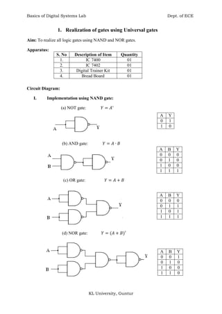
1. Basics of Digital Systems Lab Dept. of ECE
KL University, Guntur
1. Realization of gates using Universal gates
Aim: To realize all logic gates using NAND and NOR gates.
Apparatus:
Circuit Diagram:
I. Implementation using NAND gate:
(a) NOT gate:
(b) AND gate:
(c) OR gate:
(d) NOR gate:
S. No Description of Item Quantity
1. IC 7400 01
2. IC 7402 01
3. Digital Trainer Kit 01
4. Bread Board 01
A Y
0 1
1 0
A B Y
0 0 0
0 1 0
1 0 0
1 1 1
A B Y
0 0 0
0 1 1
1 0 1
1 1 1
A B Y
0 0 1
0 1 0
1 0 0
1 1 0
2. Basics of Digital Systems Lab Dept. of ECE
KL University, Guntur
(e) Ex-OR gate:
II. Implementation using NOR gate:
(a) NOT gate:
(b) AND gate:
(c) OR gate:
(d) NAND gate:
(e) Ex-NOR gate:
A B Y
0 0 0
0 1 1
1 0 1
1 1 0
A Y
0 1
1 0
A B Y
0 0 0
0 1 0
1 0 0
1 1 1
A B Y
0 0 0
0 1 1
1 0 1
1 1 1
A B Y
0 0 1
0 1 1
1 0 1
1 1 0
A B Y
3. Basics of Digital Systems Lab Dept. of ECE
KL University, Guntur
Procedure:
a) Connections are made as per the circuit diagram I & II.
b) By applying the inputs, the outputs are observed and the operation is verified with the help
of truth table.
Precautions:
1. Connections must be tight on the bread board.
2. Identify the pins of the IC properly.
3. Take care while removing and inserting the IC on bread board.
Result:
0 0 1
0 1 0
1 0 0
1 1 1
4. Basics of Digital Systems Lab Dept. of ECE
KL University, Guntur
2. Design of Combinational Logic Circuits
Aim: To design and implement combinational logic circuits like half-adder, full-adder and
half-subtractor using NAND gates.
Apparatus:
Design procedure:
The design of combinational circuits starts from verbal outline of the problem and ends in a
logic circuit diagram, or a set of Boolean functions from which the logic diagram can be
easily obtained.
The different steps involved in the design of a combinational logic circuit are as follows:
1. Statement of the problem.
2. Identification of input and output variables.
3. Expressing the relationship between the input and output variables.
4. Construction of a truth table to meet input–output requirements.
5. Writing Boolean expressions for various output variables in terms of input variables.
6. Minimization of Boolean expressions.
7. Implementation of minimized Boolean expressions using gates.
Half-Adder:
A half adder is a combinational logic circuit that performs the arithmetic addition of two bits.
Such a circuit thus has two inputs that represent the two bits to be added and two outputs,
with one producing the SUM output and the other producing the CARRY.
Truth table:
S. No Description of Item Quantity
1. IC 7400 03
2. Digital Trainer Kit 01
3. Bread Board 01
A B S C
0 0 0 0
0 1 1 0
1 0 1 0
1 1 0 1
5. Basics of Digital Systems Lab Dept. of ECE
KL University, Guntur
For Sum S: For Carry C:
The Boolean expressions for the SUM and CARRY outputs are given by the equations
Half-Adder using NAND gates
Full-Adder:
A full adder circuit is an arithmetic circuit block that can be used to add three bits to produce
a SUM and a CARRY output. Two of the input variables and represent the two
significant bits to be added and the third input represents the carry from the previous lower
significant position.
∑
∑
For Sum S: For Carry C:
X Y Z S C
0 0 0 0 0
0 0 1 1 0
0 1 0 1 0
0 1 1 0 1
1 0 0 1 0
1 0 1 0 1
1 1 0 0 1
1 1 1 1 1
6. Basics of Digital Systems Lab Dept. of ECE
KL University, Guntur
To implement a full adder using two half adders, the following expressions are used:
Full-Adder using NAND gates
Half-Subtractor:
A Half-Subtractor is a combinational circuit that can be used to subtract one binary digit from
another to produce a DIFFERENCE output and a BORROW output. The BORROW output
here specifies whether a ‘1’ has been borrowed to perform the subtraction.
Truth table
X Y D B
0 0 0 0
0 1 1 1
1 0 1 0
1 1 0 0
7. Basics of Digital Systems Lab Dept. of ECE
KL University, Guntur
Half-Subtractor using NAND gates
Procedure:
a) Connections are made as per the circuit diagrams shown.
b) By applying the inputs, the outputs are observed and the operation of logic circuits are
verified with the help of truth table.
Precautions:
1. Connections must be tight on the bread board.
2. Identify the pins of the IC properly.
3. Take care while removing and inserting the IC on bread board.
Result:
8. Basics of Digital Systems Lab Dept. of ECE
KL University, Guntur
3. Design of Magnitude Comparator
Aim: To design and implement one bit magnitude comparator using gates and 4 bit
comparator using IC 7485.
Apparatus:
Design Procedure:
The comparison of two numbers is an operation that determines if one number is greater than,
less than, or equal to the other number. A magnitude comparator is a combinational circuit
that compares two numbers, and , and determines their relative magnitudes. The outcome
of the comparison is specified by three binary variables that indicate whether
a) One Bit Magnitude Comparator:
The 1-bit comparator compares two 1 bit numbers and gives an output based on the
magnitude of two bits. The truth table for the circuit is as shown:
; ;
Fig. 1: One-bit Comparator
S. No Description of Item Quantity
1. IC 7402, 7404, 7408, 7485 01 Each
2. Digital Trainer Kit 01
3. Bread Board 01
0 0 0 1 0
0 1 0 0 1
1 0 1 0 0
1 1 0 1 0
9. Basics of Digital Systems Lab Dept. of ECE
KL University, Guntur
b) 4 Bit Magnitude Comparator using 7485:
The 7485 is a high speed, expandable 4-bit magnitude comparator which compares
two 4-bit words and generates three outputs: (A>B), (A=B) and (A<B). Three
cascading inputs allow serial expansion over any word length without external gates.
For 4-bit comparison, the cascading inputs
Fig. 2: 4-bit Comparator
Procedure:
One-bit Comparator:
1. Connections are made as per the Fig. 1.
2. By applying the inputs A & B, the output magnitude is determined and the truth table
is verified.
4-bit Comparator:
1. Connections are made as per the Fig. 2 using IC 7485.
2. Apply the comparing inputs and the output is observed for various cascading inputs
and the operation is verified with the help of truth table.
10. Basics of Digital Systems Lab Dept. of ECE
KL University, Guntur
Function Table of 7485:
Precautions:
1. Connections must be tight on the bread board.
2. Identify the pins of the IC properly.
3. Take care while removing and inserting the IC on bread board.
Result:
4. Design of Multiplexer and Demultiplexer
11. Basics of Digital Systems Lab Dept. of ECE
KL University, Guntur
Aim: To design and implement Multiplexer and using gates.
Apparatus:
Design Procedure:
A multiplexer is a combinational circuit that selects binary information from one of many
input lines and directs it to a single output line. The selection of a particular input line is
controlled by a set of selection lines. In general, there are 2n
input lines and n selection lines
whose bit combinations determine which input is selected.
Multiplexer:
There are 4 input lines and 2 select inputs .
0 0
0 1
1 0
1 1
Demultiplexer:
A demultiplexer is a circuit that receives information on a single line and transmits this
information on one of 2n
possible output lines. The selection of a specific output line is
controlled by the bit values of n selection lines.
S. No Description of Item Quantity
1. IC 7404, 7410, 7420 01 Each
2. Digital Trainer Kit 01
3. Bread Board 01
13. Basics of Digital Systems Lab Dept. of ECE
KL University, Guntur
Fig. 2: 1x4 Demultiplexer
Procedure:
Multiplexer:
1. Connections are made as per the circuit diagram 1.
2. By varying the select inputs S1 & S0, any one of the 4 inputs can be selected on the
output and the truth table is verified.
:
1. Connections are made as per the Fig. 2.
2. By varying the select inputs S1 & S0, the information on the single input E is
transmitted to any one of 4 output lines and the truth table is verified.
Precautions:
1. Connections must be tight on the bread board.
2. Identify the pins of the IC properly.
3. Take care while removing and inserting the IC on bread board.
Result:
14. Basics of Digital Systems Lab Dept. of ECE
KL University, Guntur
5. BCD to 7 Segment Decoder with Common anode display
Aim: To realize the operation of BCD to 7 segment decoder using IC 7447 and common
anode display.
Apparatus:
Circuit Diagram:
IC 7490:
The 74LS90 is a 4-bit, ripple-type decade counter. The device consists of four master-slave
flip-flops internally connected to provide a divide-by-two section and a divide-by-five
section. The device can be operated in various counting modes like BCD counter, divide-by-
five counter, divide-by-two counter and biquinary divide-by-ten counter.
S. No Description of Item Quantity
1. IC 7447, 7490, FND 542 01 Each
2. Digital Trainer Kit 01
3. Bread Board 01
15. Basics of Digital Systems Lab Dept. of ECE
KL University, Guntur
In a BCD Counter, the ̅̅̅̅̅ input must be externally connected with the output. The ̅̅̅̅̅
input receives the incoming count producing a BCD count sequence. Set
.
IC 7447:
IC 7447 is a BCD to 7 segment decoder with active low outputs. It accepts the BCD code and
provides outputs to energize seven segment display devices in order to produce a decimal
read out.
̅̅̅̅ stands for Lamp Test. When ̅̅̅̅ is low all the segments on the 7-segment display are lit
regardless of .
̅̅̅ stands for Blanking Input. When ̅̅̅ is low the display is blank so all the segments on the
7segment display are off regardless of
̅̅̅̅̅stands for Ripple Blanking Input. When ̅̅̅̅̅ is low and the display
is blank otherwise the number is displayed on the display. This is used to remove leading
zeroes from a number (e.g. display 89 instead of 089). To use with more than one display
connect (Ripple Blanking Output) from most significant 7447 to the next 7447.
For normal operation, ̅̅̅̅ ̅̅̅ ̅̅̅̅̅
16. Basics of Digital Systems Lab Dept. of ECE
KL University, Guntur
Procedure:
1. Connections are made as per the circuit diagram shown.
2. BCD inputs are applied to 7 segment decoder using IC 7490, which is a ripple
counter.
3. Apply ̅̅̅̅ ̅̅̅ ̅̅̅̅̅ to IC 7447.
4. For each clock pulse BCD number will be generated using 7490 and the ten
corresponding decimal digits can be displayed in common anode display.
Precautions:
1. Connections must be tight on the bread board.
2. Identify the pins of the IC properly.
3. Take care while removing and inserting the IC on bread board.
Result:
17. Basics of Digital Systems Lab Dept. of ECE
KL University, Guntur
6. Realization of Flip-flops using Gates
Aim: To realize the flip-flops like SR, JK, D and T Flip-flops using gates.
Apparatus:
Circuit Diagram:
Clocked SR Flip-flop:
Truth table:
JK Flip-flop:
S. No Description of Item Quantity
1. IC 7400, 7404, 7410 01 Each
2. Digital Trainer Kit 01
3. Bread Board 01
0 X X
1 0 0
1 0 1 0
1 1 0 1
1 1 1
18. Basics of Digital Systems Lab Dept. of ECE
KL University, Guntur
Truth table:
Procedure:
1. Connections are made as per the circuit diagram.
2. By applying inputs, the outputs are verified with the help of truth table.
Precautions:
1. Connections must be tight on the bread board.
2. Identify the pins of the IC properly.
3. Take care while removing and inserting the IC on bread board.
Result:
X 0 1 X X
X 1 0 X X
0 1 1 X X
1 1 1 0 0
1 1 1 0 1 0
1 1 1 1 0 1
1 1 1 1 1
19. Basics of Digital Systems Lab Dept. of ECE
KL University, Guntur
7. Design of Ripple Counters
Aim: To design and verify the operation BCD ripple counter using JK flip-flops.
Apparatus:
Design Procedure:
In ripple counter, the flip-flops within the counter are not made to change the states at exactly
the same time, i.e., they are not clocked simultaneously. In a ripple counter, also called an
asynchronous counter or a serial counter, the clock input is applied only to the first flip-flop,
also called the input flip-flop, in the cascaded arrangement. The clock input to any
subsequent flip-flop comes from the output of its immediately preceding flip-flop.
Modulus of the counter:
The number of states through which the counter passes before returning to the starting state is
called the modulus of the counter. The condition to determine the number of flip-flops is
BCD Ripple Counter: It is also known as MOD 10 ripple counter or Decade Ripple counter.
S. No Description of Item Quantity
1. IC 7400 01
2. IC 7476 02
3. Digital Trainer Kit 01
4. Bread Board 01
0 0 0 0
0 0 0 1
0 0 1 0
0 0 1 1
0 1 0 0
0 1 0 1
0 1 1 0
0 1 1 1
1 0 0 0
1 0 0 1
20. Basics of Digital Systems Lab Dept. of ECE
KL University, Guntur
Connect to a NAND gate and the output of the gate to clear input of the flip-flops.
Hence after state 1001, when the circuit enters into state 1010, the NAND output becomes 0
and hence the flip-flops will be in reset state, 0000 and the count continues.
Circuit Diagram:
Procedure:
1. Connections are made as per the circuit diagram.
2. Set preset = 1, for all the flip-flops and apply clock signal manually to the
least significant flip-flop.
3. Connect to a NAND gate and the output of the gate to clear input of the flip-
flops.
4. The flip-flops will change their state for each clock pulse and ten states are observed
before it returns to the initial state.
Precautions:
1. Connections must be tight on the bread board.
2. Identify the pins of the IC properly.
3. Take care while removing and inserting the IC on bread board.
Result:
21. Basics of Digital Systems Lab Dept. of ECE
KL University, Guntur
8. Design of Synchronous Counters
Aim: To design a counter using JK flip-flops for the following binary sequence: 0, 4, 2, 1, 6
and repeat.
Apparatus:
Design Procedure:
In a synchronous counter, also known as a parallel counter, all the flip-flops in the counter
change state at the same time in synchronism with the input clock signal. The clock signal in
this case is simultaneously applied to the clock inputs of all the flip-flops.
Circuit Excitation and output table:
S. No Description of Item Quantity
1. IC 7408, 7432 01 Each
2. IC 7476 02
3. Digital Trainer Kit 01
4. Bread Board 01
Present State (PS) Next State (NS)
0 0 0 1 0 0
0 0 1 1 1 0
0 1 0 0 0 1
1 0 0 0 1 0
1 1 0 0 0 0
Present State
(PS)
Next State (NS) Flip-flop Input functions
0 0 0 1 0 0 1 0 0
0 0 1 1 1 0 1 1 1
0 1 0 0 0 1 0 1 1
1 0 0 0 1 0 1 1 0
1 1 0 0 0 0 1 1 0
22. Basics of Digital Systems Lab Dept. of ECE
KL University, Guntur
By using K-maps, we get.
; ; ;
Procedure:
1. Connections are made as per the circuit diagram.
2. Set preset = clear = 1, for all the flip-flops and apply clock signal
manually to all the flip-flops simultaneously.
3. The flip-flops will change their state for each clock pulse and the required states are
observed before the counter returns to the initial state.
Precautions:
1. Connections must be tight on the bread board.
2. Identify the pins of the IC properly.
3. Take care while removing and inserting the IC on bread board.
Result:
23. Basics of Digital Systems Lab Dept. of ECE
KL University, Guntur
9. Shift Registers, Ring & Johnson Counter
Aim: To verify the operation of SISO shift register and Ring & Johnson counters using D
flip-flops.
Apparatus:
Circuit Diagrams:
a) 4 bit SISO shift Register:
b) 4 bit Ring Counter:
Ring Counter States:
S. No Description of Item Quantity
1. IC 7408, 7432 01 Each
2. IC 7476 02
3. Digital Trainer Kit 01
4. Bread Board 01
1 0 0 0
0 1 0 0
0 0 1 0
0 0 0 0
24. Basics of Digital Systems Lab Dept. of ECE
KL University, Guntur
c) 4 bit Johnson Counter:
Johnson Counter States:
Procedure:
4 bit SISO shift register:
1. Connections are made as per the circuit diagram (a).
2. Set preset = clear = 1 for all the flip-flops and apply clock signal manually to all the
flip-flops simultaneously.
3. Apply the data to the left-most flip-flop and for every clock pulse, data input will shift
towards right side.
4 bit Ring Counter:
1. Connections are made as per the circuit diagram (b).
0 0 0 0
1 0 0 0
1 1 0 0
1 1 1 0
1 1 1 1
0 1 1 1
0 0 1 1
0 0 0 1
25. Basics of Digital Systems Lab Dept. of ECE
KL University, Guntur
2. Set preset = clear = 1 for all the flip-flops and apply clock signal manually to all the
flip-flops simultaneously.
3. Apply logic 1 as input at the beginning and the ring counter will change its state for
every clock pulse and after 4 states, the cycle repeats.
4 bit Johnson Counter:
1. Connections are made as per the circuit diagram (c).
2. Set preset = clear = 1 for all the flip-flops and apply clock signal manually to all the
flip-flops simultaneously.
3. The Johnson counter will change its state for every clock pulse and after 8 states, the
cycle repeats and the truth table is verified.
Precautions:
1. Connections must be tight on the bread board.
2. Identify the pins of the IC properly.
3. Take care while removing and inserting the IC on bread board.
Result:
26. Basics of Digital Systems Lab Dept. of ECE
KL University, Guntur
10. Design of Two digit display using IC 7490
Aim: To design and verify the operation of BCD to 7 segment decoder using IC 7447 and
common anode display.
Apparatus:
Circuit Diagram:
Procedure:
1. Connections are made as per the circuit diagram shown.
2. Numbers from 00 to 99 can be observed using the above arrangement for every one
clock pulse.
Precautions:
S. No Description of Item Quantity
1. IC 7447, 7490, FND 542 02 Each
2. Digital Trainer Kit 01
3. Bread Board 01
27. Basics of Digital Systems Lab Dept. of ECE
KL University, Guntur
1. Connections must be tight on the bread board.
2. Identify the pins of the IC properly.
3. Take care while removing and inserting the IC on bread board.
Result: