Stick Diagram
•Download as PPTX, PDF•
12 likes•29,234 views

Introduction to Stick Diagram, VLSI Design, Any Questions related to MOS Transistor and VLSI Design, Write in the Comment Box Below.

Recommended
More Related Content
What's hot
What's hot (20)
Similar to Stick Diagram
More from Kalyan Acharjya
More from Kalyan Acharjya (20)
Recently uploaded
Recently uploaded (20)
Stick Diagram
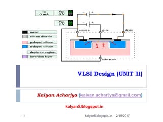
- 1. VLSI Design (UNIT II) Kalyan Acharjya (kalyan.acharjya@gmail.com) 2/19/20171 kalyan5.blogspot.in kalyan5.blogspot.in
- 2. Disclaimer 2/19/20172 All Contents are collected from various sources (Internet). Thank you to all respective original owners. Only for academic use. kalyan5.blogspot.in
- 3. UNIT 2 (MOS MODELING) STICK DIAGRAM MOS LAYOUT 2/19/20173 kalyan5.blogspot.in
- 4. Stick Diagram and Representation 2/19/20174 A stick diagram is a stick representation for the layout and represented by simple lines. It shows all components with relative placement. It does not show exact placement, transistor sizes, wire lengths, wire widths, tub boundaries. n-diffusion (device well, local interconnect) Polysilicon (gate electrode, interconnect) metal (contact, interconnect) simple contact cut depletion implant Buried contact cut Metal-1 kalyan5.blogspot.in
- 5. Mask Layout Encoding for Different Layers 2/19/20175 N Type diffusion P -Type diffusion Polysilicon Metal 1 Contact Cut Ion implantation Buried contact VDD or VSS contact kalyan5.blogspot.in
- 6. Stick Diagram 2/19/20176 Stick diagrams help plan layout quickly Need not be to scale Draw with color pencils or dry-erase markers Metal Polysilicon Metal Contact P-Doping N-Doping kalyan5.blogspot.in
- 7. Stick Diagram & Corresponding Mask Layout 2/19/20177 Layout: Do not forget the implants for depletion mode transistors and to write in the length to width (L:W) ratio for each transistor kalyan5.blogspot.in
- 8. Stick Diagram & Corresponding Mask Layout Depletion 2/19/20178 kalyan5.blogspot.in
- 9. Stick Diagram of NMOS & PMOS 2/19/20179 P-Well Area N-Well Area kalyan5.blogspot.in
- 10. N-MOS (Enhancement & Depletion) 2/19/201710 kalyan5.blogspot.in
- 11. Complete n-MOS-Stick Diagram 2/19/201711 kalyan5.blogspot.in
- 13. Layout & Stick Diagram of CMOS Inverter 2/19/201713 kalyan5.blogspot.in
- 14. Depletion Load Inverter 2/19/201714 kalyan5.blogspot.in
- 15. CMOS-2 Input NAND & NOR GATE 2/19/201715 kalyan5.blogspot.in
- 16. Stick Diagram of CMOS NAND Gate- Euler’s Path 2/19/201716 kalyan5.blogspot.in
- 18. Example 3-Eular Path: 2/19/201718 kalyan5.blogspot.in
- 19. Example 3-Stick Diagram 2/19/201719 kalyan5.blogspot.in
- 21. One More Example 2/19/201721 kalyan5.blogspot.in
- 22. BAS HO GAYA…..! 2/19/201722 Boys Girls kalyan5.blogspot.in
- 23. Thank you for your kind attention ! 2/19/201723 kalyan5.blogspot.in