
Recommended
More Related Content
What's hot
What's hot (20)
Viewers also liked
Viewers also liked (17)
Similar to Example of the Laplace Transform
Similar to Example of the Laplace Transform (20)
Example of the Laplace Transform
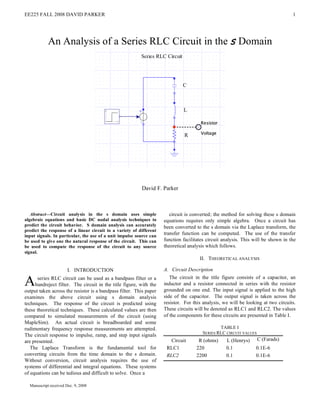
- 1. EE225 FALL 2008 DAVID PARKER 1 An Analysis of a Series RLC Circuit in the s Domain David F. Parker Abstract—Circuit analysis in the s domain uses simple circuit is converted; the method for solving these s domain algebraic equations and basic DC nodal analysis techniques to equations requires only simple algebra. Once a circuit has predict the circuit behavior. S domain analysis can accurately been converted to the s domain via the Laplace transform, the predict the response of a linear circuit to a variety of different input signals. In particular, the use of a unit impulse source can transfer function can be computed. The use of the transfer be used to give one the natural response of the circuit. This can function facilitates circuit analysis. This will be shown in the be used to compute the response of the circuit to any source theoretical analysis which follows. signal. II. THEORETICAL ANALYSIS I. INTRODUCTION A. Circuit Description A series RLC circuit can be used as a bandpass filter or a bandreject filter. The circuit in the title figure, with the output taken across the resistor is a bandpass filter. This paper The circuit in the title figure consists of a capacitor, an inductor and a resistor connected in series with the resistor grounded on one end. The input signal is applied to the high examines the above circuit using s domain analysis side of the capacitor. The output signal is taken across the techniques. The response of the circuit is predicted using resistor. For this analysis, we will be looking at two circuits. these theoretical techniques. These calculated values are then These circuits will be denoted as RLC1 and RLC2. The values compared to simulated measurements of the circuit (using of the components for these circuits are presented in Table I. MapleSim). An actual circuit is breadboarded and some rudimentary frequency response measurements are attempted. TABLE I SERIES RLC CIRCUIT VALUES The circuit response to impulse, ramp, and step input signals are presented. Circuit R (ohms) L (Henrys) C (Farads) The Laplace Transform is the fundamental tool for RLC1 220 0.1 0.1E-6 converting circuits from the time domain to the s domain. RLC2 2200 0.1 0.1E-6 Without conversion, circuit analysis requires the use of systems of differential and integral equations. These systems of equations can be tedious and difficult to solve. Once a Manuscript received Dec. 9, 2008
- 2. EE225 FALL 2008 DAVID PARKER 2 B. The Laplace Transform Substituting the values in RLC1, we have The Laplace transform of a function is given by the 2200s H (s) = (6) expression s + 2200s + 10 8 2 Likewise, for RLC2 we have " 22000s L{ f (t)} = # f (t)e! st dt (1) H (s) = (7) 0 s + 22000s + 10 8 2 The Laplace transform of f (t) is also denoted F(s) where If we factor the denominator of equations (6) and (7), this F(s) = L { f (t)} . (2) reveals the poles of the transfer function. The poles are The notation used in equation 2 will be employed in the defined as the roots of the denominator. For RLC1, remainder of this paper. In order to analyze a circuit in the s 2200s H (s) = (8) domain, each of the circuit elements must be transformed to the s domain. Table II shows these transformations. Phasor (s+1100+9939I) ( s + 1100 ! 9939I ) domain transformations are also shown. and for RLC2, we have 22000s H (s) = (9) TABLE II CIRCUIT ELEMENT TRANSFORMATIONS (s+15582 ) ( s + 6417 ) t phasor s The poles are indicators of the circuit’s response to an input R R R signal. If the poles are complex as in RLC1, the circuit will L j! L sL oscillate. If the poles are real as in RLC2, then the circuit 1 decays with an exponential function. 1 C j! C sC D. The Expression of Vo(s) & Vo(t)-output Based on equation (3), we know that the s domain output of a circuit can be expressed as C. The Transfer Function Y (s) = H (s)X(s) (10) The transfer function is defined as the s domain ratio of the Laplace transform of the output to the Laplace transform of If we know the transfer function of a circuit ( H (s)) and we the input. The transfer function is apply a known input signal ( X(s)) , we can calculate the H (s) = Y (s) (3) output (Y (s)) . This is also known as Vo(s). If we perform X(s) the inverse Laplace transform on this, we have Vo(t)-the whereY (s) is the Laplace transform of the output signal output signal in the time domain. The process of returning to the time domain is known as the inverse Laplace transform, and X(s) is the transform of the input signal. With this transfer function the output signal (response) of the circuit can L! {F(s)} = f (t) . be easily determined based on the input signal. If we employ this equation with the series RLC circuit studied, we have III. FREQUENCY RESPONSE R H (s) = (4) The transfer function of a bandpass filter is expressed as 1 R + sL + !s sC H (s) = (11) In order to facilitate analysis of this transfer function, we s + !s + "0 2 2 need to put it in standard form. The transfer function in where ! is the bandwidth (radians/s) and ! 0 is the center equation (4) is expressed in the standard form where the frequency (radians/s). If we examine equation (5) and let highest order s term in the denominator is isolated from any coefficients and each term after that is given in decreasing R 1 != , then we can see that ! 0 = . It is clear that order. For this equation, if we multiply the numerator and the L LC s the transfer function of both RLC1 and RLC2 show that they denominator by , this will do this. The result is L are bandpass filters. ! c1 , the lower cutoff frequency ! R$ (radians/s) of this filter can be expressed as # &s " L% # $ #' 2 H (s) = (5) ! c1 = " + & ) + !0 . 2 (12) ! R$ 1 2 % 2( s2 + # & s + " L% LC The cutoff frequency is defined as the frequency where the
- 3. EE225 FALL 2008 DAVID PARKER 3 1 magnitude of the output = Vi . Knowing ! and ! c1 , the Table III shows the calculated values of ! 0 , ! c1 , and ! c2 , 2 upper cutoff frequency can be determined by simulated values of ! c1 , ! c2 ,as well as values measured ! c2 = ! c1 + " (13) with a breadboard circuit. The values marked with a ‘*’ I was unable to measure with my rudimentary measurement setup. Table III circuit Calculated values Simulated values Measured values ω0 ωc1 ωc2 ωc1 ωc2 ωc1 ωc2 RLC1 10000 8960 11160 8800 11000 6300 17000 RLC2 10000 3866 25866 3900 25000 * * increases, bandwidth increases as well. Again this agrees R with the equation != , as discussed before. L IV. IMPULSE RESPONSE The Laplace transform of several functions discussed in this paper are presented in Table IV. TABLE IV LAPLACE TRANSFORMS Type f (t)(t > 0 ! ) F(s) Impulse ! (t) 1 1 Ramp t s2 1 Step u(t) s The impulse response is the signal that exits a system when a delta function (unit impulse) is the input. An impulse is a signal composed of all zeros, except a single nonzero point. For our analysis, in order to see the response of the circuit to an impulse, all we need to do is multiply the transfer function of the circuit by 1 (see Table IV and equation (10). Then one performs the inverse Laplace transform to get back to the time domain. In order to facilitate this, we first perform a Partial Fraction Expansion of the transfer function. For RLC1, the result of this operation on equation (8) is 1106.7! + 6.3! 1106.7! " 6.3! Y (s) = + (14) s + 1100 " 9939I s + 1100 + 9939I Figure 1 and 2 show Bode plots of the two bandpass circuits. One can see that the frequency response of RLC2 is and for RLC2 –equation(9) is much more broad and the phase response change is much 37404.3 15404.3 Y (s) = ! (15) more gradual than RLC1. The peak in the frequency response (s+15582.) s+6417.4 plot is the same for both circuits. This agrees with our analysis in that the center frequency is dependent only on the The rules for performing the inverse transform of the above values of the inductor and the capacitor. As the value of R
- 4. EE225 FALL 2008 DAVID PARKER 4 two forms are given in Table V. TABLE V TWO USEFUL TRANSFORM PAIRS Nature of F(s) f (t) Roots K Distinct real Ke! at u(t) s+a Distinct K K* + 2 K e!" t cos(# t + $ )u(t) Complex s + ! " #I s + ! + #I Applying the above rules, we have for RLC1 The above simulations appear to confirm our calculations. Vo(t) = " 2213e !1100t cos(9939t + 6.3 ) $ u(t) (16) ! Note that the period of oscillations in Figure 3 appears to have # % the same period as the resonant frequency calculated earlier in and for RLC2 the frequency response section of this paper. Vo(t) = ! 37404.4e-15582t -15404.3e-6417t # u(t) (17) " $ V. RAMP RESPONSE These two equations indicate the impulse response of the circuits. For RLC1, we have what appears to be a damped oscillation. For RLC2, we have a decaying exponential. Again, per Table IV and equation (10), we can calculate the Figures 3 and 4 show the simulated impulse response. circuit response to a ramp input. One simple needs to multiply the transfer function by the s domain representation of a ramp, ! 1$ # 2 & . For RLC1 using equation(8), this gives us "s % 2200s " 1% (s+1100+9939I) ( s + 1100 ! 9939I ) $ s 2 ' . # & For RLC2 using equation(9), this gives us 22000s ! 1$ (s+15582 ) ( s + 6417 ) # s 2 & . After Partial Fraction " % Expansion (PFE) of the result and use of the rules in Table V for transforming back to the time domain we have for RLC1 Vo(t) = " 2.2x10 !5 + 2.2x10 !5 e!1100t cos(9939t + 174 ! ) $ u(t) # % (18) and for RLC2 Vo(t) = " 2.2x10 !4 + 1.54x10 -4 e-15582t ! 3.74x10 -4 e-6417t $ u(t) # % (19) Figures 5 shows the simulated ramp input. Figures 6 and 7 show the response to this input. Again, RLC1 shows the characteristic oscillation or ringing at the approximate resonant frequency. RLC2 shows a decaying exponential.
- 5. EE225 FALL 2008 DAVID PARKER 5
- 6. EE225 FALL 2008 DAVID PARKER 6 VI. STEP RESPONSE We can calculate , per Table IV and equation (10), the circuit response to a step input. One simple needs to multiply the transfer function by the s domain representation of a step, ! 1$ # & . For RLC1 using equation (8), this gives us " s% 2200s " 1% (s+1100+9939I) ( s + 1100 ! 9939I ) $ s ' . # & For RLC2 using equation (9), this gives us 22000s ! 1$ (s+15582 ) ( s + 6417 ) # s & . After Partial Fraction " % Expansion (PFE) of the result and use of the rules in Table V for transforming back to the time domain we have for RLC1 Vo(t)= !.2213e-1100t cos(9939t+90! ) # u(t) " $ (20) and for RLC2 Vo(t) = ! 2.4e-6417t -2.4e-15582t # u(t) " $ (21) Figures 8 shows the simulated step input. Figures 9 and 10 show the response to this input. VII. CONCLUSIONS Circuit analysis in the s domain is useful because it allows one to use simple algebra to solve transient response problems. Otherwise, one would have to use complex systems of differential equations. Using the unit impulse source to drive a circuit facilitates analysis of the circuit because this input yields the natural response of the circuit. The unit impulse response of a circuit contains enough information to compute the response of the circuit to any input signal. Measurements made with a small breadboard circuit did not agree very well with simulated or calculated values because the equipment the author used-a $30 signal generator and a NI DAQ with LabView did not have enough accuracy at the higher test frequencies used.