1. An X-band GaN PA MMIC for Phased Array Radar
Applications
Stuart Glynn and Liam Devlin
Plextek RFI, The Plextek Building, London Road, Great Chesterford, Saffron Walden, CB10 1NY, UK;
(liam.devlin@plextekRFI.com)
Abstract
Active phased array radars require numerous Power Amplifiers (PAs), which must be small, efficient
and low-cost. This paper describes an X-band PA MMIC that covers 9 to 11.5GHz and satisfies these
requirements. It has an output power of 7W (38.5dBm) from a 29dBm drive with a Power Added
Efficiency (PAE) of 42%. The design was realized on the 0.25µm gate length GaN on SiC process of
UMS (GH25) using Keysight’s ADS 2015. The die size is just 1.5mm x 2mm, which means around
2,300 PAs can be fabricated on a single 4” diameter wafer.
Introduction
Phased array radars use many transmitters operating in parallel to generate a high total transmitted
RF power level. The RF amplifier at the output of each transmitter must be capable of generating the
required RF power and must do so efficiently and at an acceptable cost. The elements must be
closely spaced (normally around a half wavelength separation) and this fact, coupled with the
potentially huge level of total dissipated power, can represent enormous challenges for the radar
design team. The PA is normally the key contributor to the power dissipation so a component with
high efficiency is very desirable.
Typical RF power levels required from each transmitting element are in the range 5 to 10W. GaN
technology can realise such power levels with ease and can do so with high efficiency. The amplifier
described here was designed to realise the output stage with adequate gain to allow the input drive
to be provided by readily available COTS technology. The target performance requirements for the
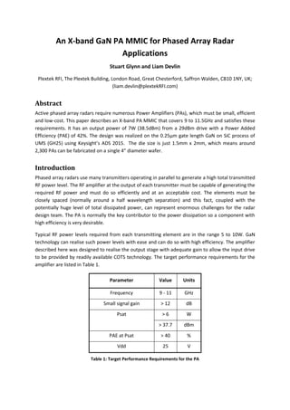
amplifier are listed in Table 1.
Parameter Value Units
Frequency 9 - 11 GHz
Small signal gain > 12 dB
Psat > 6 W
> 37.7 dBm
PAE at Psat > 40 %
Vdd 25 V
Table 1: Target Performance Requirements for the PA
2. Design and Layout
The PA was designed for realisation on the 0.25µm gate length GaN on SiC process of UMS (GH25).
The design process commenced with simulations at the transistor level to determine the preferred
transistor size and bias. The RF output power that a transistor can generate increases as the total
gate periphery increases. However, as the physical size of the transistor starts to become electrically
significant both the large signal and small signal performance will start to degrade as a result of
distributed parasitics. Microwave frequency PAs normally make use of multiple power combined
transistors for this very reason and the impact on performance of the transistor’s size must be
carefully considered.
Another factor to consider in selecting the optimum transistor size is the range of validity of the
transistor models. Commercial foundries normally have Process Design Kits (PDKs) that include
scaleable transistor models. Whilst the models may allow arbitrary adjustment of gate width and
number of fingers, the models will be based on data from a selection of transistors of discrete sizes.
It is best to try and select a transistor size that does not require too much extrapolation from the
sizes of transistors used to generate the models.
With these factors in mind an 8x150µm transistor was selected for the planned design. The
recommended Vds for GH25 transistors is 25V; simulations were undertaken comparing Psat, PAE,
and available gain at various quiescent bias currents. Figure 1 shows an example set of load-pull
contours. The Psat (at 4dB compression) for the selected transistor size was around 36.5dBm (4.4W)
and varied only modestly with the quiescent bias. The PAE improved with reducing quiescent bias
current but the small signal gain decreased. The design was progressed with a quiescent bias
currents Ids of 45mA (37.5mA/mm); the performance with a higher bias current of 90mA
(75mA/mm) was reviewed during the design process to assess the performance benefits that a
higher bias current could potentially offer.
A design with two power combined 8x150µm transistors was progressed. Allowing for the losses of
the on-chip biasing and matching networks, this would still allow the target 6W (37.7dBm) minimum
output power requirement to be exceeded.
Further detailed load-pull simulations were then undertaken on the selected transistor. The power
delivered to the load at 4dB compression was plotted against PAE at 10GHz for a range of load
impedances (Figure 2). Each trace in Figure 2 represents a constant real part of the load impedance
with a varying imaginary part. This analysis was used to select the optimum load impedance of 11.25
+ j21.67Ω that was used as the target during the design process.
3. Figure 1: Load-pull simulations on the 8x150µm transistor using ADS 2015
Figure 2: Simulated PAE and Pout for various fundamental load impedances
The design approach was to power combine the RF outputs of two of the selected transistor.
Throughout the design process effort was expended on ensuring that the die area was minimized.
This can be clearly seen from the layout plot reproduced in Figure 3.
Duplicate on-chip drain biasing networks are included at top and bottom of the IC. This preserves
symmetry and allows the PA to be biased from either side. The transmission line used to provide the
4. drain bias is also used as inductive matching at the drain of each transistor to allow the optimum
inductive load impedance to be presented to the transistor.
High impedance series lines are used at each transistor output to transform the common 50Ω load
impedance at the output of the PA to the lower impedance required at the transistors’ drains to
present the optimum real part of the load at each transistor output.
The input matching network is a low-pass structure that transforms the low impedance at the
transistors’ input to a 50Ω impedance at the PA input. On-chip balancing resistors are included
between the two PA channels to ensure odd-mode stability. On-chip RC de-coupling is included at
both gate and drain to ensure low frequency stability where the GaN transistors have a very high
level of available gain.
Figure 3: Layout plot of the X-band GaN PA
Realisation and Measured Performance
A photograph of one of the PA die is shown in Figure 4. The die measures just 1.5mm x 2mm, which
means that a single 4” diameter wafer should contain around 2,300 amplifier ICs.
5. Figure 4: Die photograph of the X-band GaN PA
The s-parameters of 40 amplifiers measured on wafer at a bias of 25V Vds and 90mA Ids are plotted
in Figure 5. The small signal gain is 14dB at 9GHz dropping to 12.1dB at 11GHz. A comparison of the
measured to modelled small-signal performance is plotted in Figure 6. The measured results are the
dotted traces and the modelled (simulated) performance is the solid traces. It can be seen that there
is a slight shift up in frequency of the measured performance compared to the modelled but the
agreement is good.
The large signal performance was also measured RFOW. This was measured under pulsed operation
at a duty cycle of 10% with a pulse width of 25µs. The measured results are plotted in Figure 7 for RF
input powers of 5dBm, 19dBm, 29dBm and 32dBm at a quiescent bias of 25V, 90mA. With an input
power of 29dBm the RF output power is around 38.5dBm or 7W.
A corresponding plot of the PAE (Power Added Efficiency) is shown in Figure 8. At an input drive of
29dBm the PAE is around 42% from 9 to 11.5GHz with a peak value of 48%.
6. Figure 5: Measured s-parameters of 40 devices biased at 25V, 90mA
Figure 6: Comparison of measured to modelled s-parameters at 25V, 90mA bias
7. Figure 7: RFOW measured output power (10% duty, 25µs PW) for input powers of 5dBm, 19dBm, 29dBm and
32dBm at a quiescent bias of 25V, 90mA
Figure 8: RFOW measured PAE (10% duty, 25µs PW) for input powers of 5dBm, 19dBm, 29dBm and 32dBm
at a quiescent bias of 25V, 90mA
The measured and simulated power transfer characteristics at 9.7GHz are plotted in Figure 9,
demonstrating very good agreement.
8. Figure 9: Measured and modelled power transfer characteristics at 9.7GHz
Summary and Conclusions
Details of the design, realisation and measured performance of a 9 to 11.5GHz GaN PA MMIC have
been presented. The amplifier was realised on the GH25 GaN MMIC process of UMS and designed
using the UMS PDK on ADS 2015. It was designed with active phased array radars in mind and
generates an RF output power of 38.5dBm (7W) from an input drive of 29dBm with a PAE of 42%.
Quiescent bias is 25V and 90mA. A summary of the measured performance of the GaN PA is
presented in Table 2.
Parameter Units Measured Comments
Frequency Range GHz 9-11.5
Small-signal gain dB ~13
Input return loss dB > 8
Output return loss dB > 8
Psat W (dBm) ~ 7 (38.5) +29dBm drive
PAE at Psat % ~ 42 +29dBm drive
LS gain flatness dB ±0.5
Table 2: Performance summary of the GaN PA MMIC