
Recommended
More Related Content
What's hot
What's hot (20)
Similar to Single phase AC circuits
Similar to Single phase AC circuits (20)
Recently uploaded
Recently uploaded (20)
Single phase AC circuits
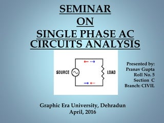
- 1. SEMINAR ON SINGLE PHASE AC CIRCUITS ANALYSIS Presented by: Pranav Gupta Roll No. 5 Section C Branch: CIVIL Graphic Era University, Dehradun April, 2016
- 2. CONTENTS 1. AC CIRCUIT 1.1 PURELY RESISTIVE CICUIT 1.2 PURELY INDUCTIVE CIRCUIT 1.3 PURELY CAPACITIVE CIRCUIT AC SERIES CIRCUITS 1.4 SERIES R-L CIRCUIT 1.5 SERIES R-C CIRCUIT 1.6 SERIES R-L-C CIRCUIT
- 3. CONTENTS • 2. RESONANCE • 2.1 RESONANCE IN SERIES • 2.2 RESONANCE IN PARALLEL • 2.3 RESONANCE FREQUENCY VARIATION OF DIFF. QUANTITIES WITH FREQUENCY 2.5 INDUCTIVE REACTANCE 2.6 CAPACITIVE REACTANCE 2.7 CURRENT
- 4. Introduction AC CIRCUIT: Circuits in which currents and voltages vary sinusoidally i,e vary with time are called alternating current or a.c circuits. All a.c circuits are made up of combination of resistance R , inductance L and capacitance C. The circuit elements R,L and C are called circuit parameters . To study a general a.c circuit it is necessary to consider the effect of each seperately.
- 5. 1.1 Purely Resistive Circuits • Figure shows a circuit containing only resistance R • v = Vm sin ωt • By Ohm’s law, the instantaneous current in the circuit will be • i =v/R =Vm sinωt / R • Vm ^/ R = Im • i=Im sinωt • Comparison of voltage equation and current shows that the phase difference are in phase difference between voltage and current is zero . Hence , in a circuit with resistance only the voltage and current are in phase with each other .
- 6. The waveform and phase diagram respectively of the voltage and current in a circuit containing only a resistance . Since maximum value = √2 * r.m.s. Value Im = √2 I: Vm = √2 V √2 V/R = √2 I V = RI Above eq=n represents ohm’s law It is noted that applied voltage is counter balanced by the voltage drop across the resistance R . This voltage drop is called resistive voltage drop and denoted by Vr . Vr = V Vr = IR
- 7. 1.2 Purely Inductive Circuit • Consider a purely inductive circuit containing only an inductance L . Let the current taken by the circuit be I = Imsinωt This current produces a self induced e.m.f. eL in the circuit given by eL= -L di/dt At any instant two voltages are present in the circuit , one is the applied voltage eL . By KVL v = - eL = L di/dt = L d(Imsin ωt)/dt = ωLImcosωt = ωLImsin(ωt+ 900) If ωLIm = Vm v = Vm sin(ωt+ 900) Comparison shows that the phase difference between voltage and current is 90 .
- 8. • If Φ is measured from the current phase Φ = +900 . • Hence , in a purely inductive circuit the voltage leads the current by 900 or the current lags by 900. • The waveform and phasor diagram respectively of the voltage and current containing only on inductance .
- 9. Inductive Reactance ωL( I I) = V ωL = V/I The quantity ωL is the ratio of the r.m.s. voltage to r.m.s. current in purely inductive circuit . It is called the inductive reactance of the circuit and is denoted by the symbol XL . Since it is the ratio of voltage and current it is measured in ohms . The opposition of inductance to the flow of alternating current is defined as the inductive reatance XL .
- 10. XL = ωL = 2 πfL Also , V = XL I The voltage drop across the inductance L is called the inductive voltage drop . It is denoted by VL . VL = V VL = XL I
- 11. 1.3 Purely Capacitive circuit • Consider a purely capacitive circuit containing only a capacitor C connected to an a.c. Supply voltage given by • v= Vmsin ωt • The current in the circuit at any instant is • i =dq/dt • i =d (Cv)/dt = C dv/dt = C d(Vm sinωt)/dt • = ωCVm cos ωt = ωCVm sin(ωt+900) • ωCVm ^ = Im • i = Im sin(ωt+900)
- 12. Comparison shows that the phase difference Φ between the voltage and the current is 900. if Φ is measured from the voltage phasor Φ = +900.Hence in purely capacitive circuit current leads the voltage by 900.The waveforms and phasor diagram respectively for a circuit containing capacitance alone.
- 13. Capacitive Reactance • ωC( √2V)= √2I • V/I=1/ωC • The ratio of r.m.s. Voltage to r.m.s. Current in a purely capacitive circuit is called the capacitive reactance. It is defined as the opposition offered by a purely capacitive circuit to the flow of sinusoidal current. The capacitive reactance is denoted by Xc and is measured in ohms. • Xc= 1/ωC= 1/2πfC • V/I= X • V= XcI • The part of the supply which charges the capacitor is known as the capacititve voltage drop. • Vc= V • Vc= XcI
- 14. 1.4 Series R-L Circuit • Consider a circuit containing a resistance R and an inductance L in series • Let V = supply voltage • I = circuit current • VR = voltage drop across R = RI • VL = voltage drop across L = XLI= 2πfLI • ΦL = phase angle between I and V • Since I is common to both elements R and L,this is used as reference phasor. The voltage VR is in phase with I and VL leads by 900 . The voltage V is the phasor sum of VR and VL that is the phasor diagram:
- 15. • The triangle having VR,VL and V as its sides is called voltage triangle for a series R-L circuit: • The phase angle ΦL between the supply voltage V and the circuit current I is the angle between the hypotenuse and the side VR .It is seen that the current I is lagging behind the voltage V in an R-L circuit. • V2 = V2 R + V2 L • = (RI)2 + (XL I)2 • V2/I2 = R2 + X2 L • V/I = √(R2 + X2 L) • ZL = √(R2 + X2 L) • ZL is called the impedance of a series R-l circuit • ZL = V/I • V = ZL I
- 16. Impedance Triangle for a Series R- L Circuit • If the length of each side of the voltage triangle is divided by current I , the impedance triangle is obtained . The impedance triangle for a series R-L circuit is given. The following results may be found from an impedance triangle for a series R-L circuit: • ZL = √(R2 + X2 L) • R = ZLcosΦL • XL = ZL sinΦL • tanΦL = XL /R
- 17. 1.5 Series R-C Circuit • A circuit containing a resistance R and a capacitance C in series • Let V = supply voltage • I = circuit current • VR = voltage drop across R = RI • VC = voltage drop across C =XCI = I/2πfC • ΦC = phase angle between I and V • The voltage VR is in phase with I and VC lags I by 900 .The voltage sum is: • V = VR + VC
- 18. The phasor diagram: The triangle having VR , Vc and V as its side is called voltage triangle for a series R-C circuit. The phase angle ΦC between the supply voltage and the circuit current is the angle between the hypotenuse and the side VR . It is observed : V2 = V2 R + V2 c = (RI)2 + (Xc I)2 V2/I2 = R2 + X2 c V/I = √(R2 + X2 c) Zc = √(R2 + X2 c) Zc is called the impedance of a series R-C circuit Zc = V/I V = Zc I
- 19. Impedance Triangle for a Series R- C Circuit If the length of each side of the voltage triangle is divided by current I , the impedance triangle is obtained . The impedance triangle for a series R-C circuit is given. The following results may be found from an impedance triangle for a series R-C circuit: ZC = √(R2 + X2 C) R = ZCcosΦC XC = ZC sinΦC tanΦC = XC /R
- 20. 1.6 Series RLC circuit A circuit having R, l and C in series is called a general series circuit current is used as reference phasor in series circuit since it is common to all the elements of circuit. There are four voltages VR in phase with I VL leading I by 900 VC lagging I by 900 Total voltage V = VR + VL + VC
- 21. Phasor diagram: VL and VC are in opp. Directions and their resultant is their arithmetic differnce There are 3 possible cases in series RLC circuit a. VL > VC i.e; Xl > XC b. VL < VC i.e; Xl < XC c. VL = VC i.e; Xl = XC
- 22. • When XL > XC the circuit is predominantly inductive . • # Inductive circuits cause the current ‘lag’ the voltage. • V=I √[R2 + ( Xl - XC )2] • Z = √[R2 + ( Xl - XC )2] • When XL < XC the circuit is predominately capacitive. • # Capacitive circuits cause the current to ‘lead’ the voltage. • V=I √[R2 + ( Xc - Xl )2] • Z = √[R2 + ( Xc - XL )2]
- 23. Impedance Triangle for RLC circuit If the length of each side of a voltage triangle is divided by current I, the impedance triangle is obtained. The impedence triangle for series RLC circuit :
- 24. 2. RESONANCE • Resonance is a condition in an RLC circuit in which the capacitive and inductive reactance are equal in magnitude, thereby resulting in a purely resistive impedance. • At resonance, the impedance consists only resistive component R. • The value of current will be maximum since the total impedance is minimum. • The voltage and current are in phase. • Maximum power occurs at resonance since the power factor is unity • Resonance circuits are useful for constructing filters and used in many application.
- 25. 2.1 Series Resonance Circuit
- 26. 2.2 Resonance in series RLC circuit CLTotal jX-jXRZ R V Z V I m Total s m Total impedance of series RLC Circuit is At resonance The impedance now reduce to CL XX RZTotal )X-j(XRZ CLTotal The current at resonance
- 28. At resonance, currents IL and IC are equal and cancelling giving a net reactive current equal to zero. Then at resonance the above equation becomes.
- 29. We remember that the total current flowing in a parallel RLC circuit is equal to the vector sum of the individual branch currents and for a given frequency is calculated as:
- 30. 2.4 Resonance Frequency Resonance frequency is the frequency where the condition of resonance occur. Also known as center frequency. Resonance frequency rad/s LC 1 ωo Hz LC2 1 of
- 31. VARIATION OF DIFFERENT QUANTITIES WITH FREQUENCY
- 32. 2.5 Variation of inductive reactance with frequency The inductive reactance XL =2∏fL is directly proportional to the frequency f .Hence its graph is a straight line through the origin
- 33. 2.6 Variation of capacitive reactance with frequency The capacitive reactance XC =1/2πfC is inversely proportional to the frequency . Hence its graph is a rectangular hyperbola XL versus f and XC versus f curves cut at a point where f=f0
- 34. 2.7 Variation of current with frequency The current versus frequency is known as resonance curve or response curve . The current has a maximum value at resonance given by I0 = V/R. The value of I decreases on either sides of the resonance
- 35. THANK YOU