SlideShare uma empresa Scribd logo
1 de 98
1/ 98
ABSTRACT
The levitation system controls the magnetic field generated by an electromagnet to levitate a
small magnet in mid-air. The levitation involve the stability of levitating material at a level.
The level can be decided or can be adjusted by using any reference voltages. The position of
material can be influenced by various factors like temperature, air or any other disturbances.
But the stability can be achieved by using sensors. The system accomplish a ferromagnetic
magnet will float in mid-air, which essentially means cancelling the force of gravity that’s
acting upon it. The force of gravity upon any mass is “F=mg” which is a linear function of
mass. So in order to levitate a magnet, one can apply magnetic field on it and try to pull it up
in opposite direction of the gravity. If the force because of the pull is exactly equal to the
force of gravity, the net difference would be zero and the object will therefore not move in
any direction and stay exactly where it is.
The small magnet levitates in the air indefinitely without any disturbance. The vertical
position of the levitating magnet is measured using a linear Hall Effect sensor and the current
in the electromagnet is controlled using a digital signal controller. The system has circuit
which provides a feedback to the PWM generator. The current through the coil is controlled
by the PWM waves. The Variation in position of the levitating material can be sensed and
maintained by varying the current through the coil.
P a g e | 2
CONTENTS
Pag
CHAPTER 1 INTRODUCTION
1.1 BASICS OF MAGNETIC LEVITATION
1.2 TYPES OF MAGNETS
1.3 DEFINITION OF MAGNETIC LEVITATION
1.3.1 Magnetic Levitation
1.3.2 Magnetic Suspension
1.3.3 Area of Attraction
1.3.4 Uses
1.3.5 Issues
CHAPTER 2 BLOCK DIAGRAM OF PROJECT
2.1 CONTROLLER
2.2 COIL DRIVER
2.3 SOLENOID
2.4 HALL EFFECT SENSORS
2.5 FEEDBACK SYSTEMS
2.6 IR SENSOR
CHAPTER 3 CIRCUIT DIAGRAM AND COMPONENTS USED
3.1 CIRCUIT DIAGRAM
3.2 WORKING
3.3 POWER SUPPLY
3.4 COMPONENTS DISCRIPTION
3.4.1 DIP (KA7500C):
3.4.2 DIFFERENTIAL AMPLIFIER Op -AMP
3.4.3 HALL EFFECT SENSORS
P a g e | 3
3.4.4 MOSFET
3.4.4.1 Composition
3.4.4.2 Operation of Mosfet
3.4.5 VOLTAGE REGULATOR:
3.4.6 ELECROMAGNET
3.4.7 POTENTIOMETER
3.4.8 CAPACITORS
3.4.9 RESISTORS
3.4.10 DIODES
3.5 DATASHEETS
CHAPTER 4 ADVANTAGES AND IMROVEMENTS
CHAPTER 5 CONCLUSION AND FUTURE SCOPE
REFFERENCES
P a g e | 4
LIST OF FIGURES
Fig. No Figures Name Page no
Fig 1.1 Michael Faraday 3
Fig 1.2 Induced Current from Change in Magnetic Field 4
Fig 1.3 Heinrich Lenz 5
Fig 1.4 Perpendicular Force from Induce Current 6
Fig 1.5 Permanent Magnet Fields 7
Fig 1.6 Electromagnet 9
Fig 1.7 Magnetic levitation 10
Fig 1.8 Magnetic Suspension 11
Fig 1.9 Maglev Train 11
Fig 1.10 Contactless Melting 12
Fig 1.11 Magnetic Bearing 12
Fig 1.12 Product Display 13
Fig 2.1 Block Diagram 14
Fig 3.1 Circuit Diagram 18
Fig 3.2 DIP KA7500C 25
Fig 3.3 Pin diagram of KA7500C 26
Fig 3.4 Op-amp LM741 30
Fig 3.5 Pin out of LM741 30
Fig 3.6 Difference Amplifier. 31
Fig 3.7 Working of Op-amp on bread board 32
Fig 3.8 Hall sensor 33
P a g e | 5
Fig 3.9 Working of hall effect sensors 34
Fig 3.10 Effect of magnets on the hall effect sensors. 36
Fig 3.11 MOSFET IRF540 40
Fig 3.12 Voltage Regulator 41
Fig 3.13 Industrial electromagnet lifting scrap iron 44
Fig 3.14 Electromagnets 46
Fig 3.15 Material levitating 46
Fig 3.16 Potentiometer 47
Fig 3.17 Diagramatic form of potentiometer 47
Fig 3.18 Single-turn potentiometer with metal casing removed to
expose wiper contacts and resistive track 48
Fig 3.19 Paper capacitors 53
Fig 3.20 Ceramic Capacitors 54
Fig 3.21 Electrolytic capacitor 54
Fig 3.22 Symbol of resistors 55
Fig 3.23 Resistors 55
Fig 3.24 P-N junction diode 58
Fig 3.25 Schottky Diodes 59
Fig 3.26 Test Circuit 64
Fig 3.27 Operational Waveforms 65
CHAPTER 1
INTRODUCTION
P a g e | 6
Some forces in this world are almost invisible to the naked eye and most people throughout the
world do not even know they exist. On one side it can be said that some of these forces are
abstract feelings inside of a human being that have been given names from man. These forces
could be things like emotion, guilt, and even ecstasy. On the other side it have solid concrete
principles determine how the world works. These too have been given names by man, but these
principles are not abstract and have solid ground in science. These different principles are things
like gravity, electricity, and magnetism. Magnetism has been a part of the earth since the
beginning whether people realize it or not. It is due to the magnetism of the earth that the world
spins and thus creates things like gravity. The magnetism is created by the processes within the
core of the earth. The earth’s iron-ore core has a natural spinning motion to it inside which
creates a natural magnetic force that is held constant over the earth. This creates magnetic forces
that turn the earth into a large bar magnet. The creation of North and South poles on the earth
are due to this field.
From this magnetic field, things such as the aurora borealis can be seen that is a small
electromagnetic storm in the atmosphere which creates a display for all to see. Not only does
magnetism provide the world with amazing natural displays, but it also provides the world with
amazing applications to society. One of these applications is magnetic levitation. Magnetic
levitation uses the concept of a magnets natural repulsion to poles of the same kind. This
repulsion has been harnessed and controlled in an environment to help create a system of
transportation that is both economically sound and faster then most methods of transportation at
this point.
In 1965 the Department of Commerce established the High Speed Ground Transportation Act.
Most early work on developing Maglev technology was developed during this time. The earliest
work was carried out by the Brookhaven National Laboratory, Massachusetts Institute of
Technology, Ford, Stanford Research Institute, Rohr Industries, Boeing Aerospace Co., and the
Garrett Corporation. In the United States, though, the work ended in 1975 with the termination
of Federal Funding for high-speed ground transportation and research. It was at that time when
the Japanese and German developers continued their research and therefore came out with the
first test tracks.
P a g e | 7
1.1 BASICS OF MAGNETIC LEVITATION
Magnetic Fields
The creation of magnetic forces is the basis of all magnetic levitation. The creation of a magnetic
field can be caused by a number of things. The first thing that it can be caused by is a permanent
magnet. These magnets are a solid material in which there is an induced North and South pole.
These will be described further a little later. The second way that a magnetic field can be created
is through an electric field changing linearly with time. The third and final way to create a
magnetic field is through the use of direct current.
There are two basic principles in dealing with the concept of magnetic levitation. The first law
that is applied was created by Michael Faraday. This is commonly known as Faraday’s Law.
Fig 1.1 Michael Faraday
P a g e | 8
This law states that if there is a change in the magnetic field on a coil of wire, there is seen a
change in voltage. Taking that a bit further, it could be said that if there was a change in voltage,
then there would be a change in magnetic field. This occurs in the coil when there is a current
induced as a result of that change in voltage. From Figure 1.2 below it is illustrated that the
change in the magnetic field produces a current.
Fig 1.2 Induced Current from Change in Magnetic Field
For the purposes of magnetic levitation the ability to change the strength of a magnetic field by
just changing the current is powerful. If there is a need for more of a force, then sending more
current through a coil of wires will produce more of a greater magnetic force.
The direction of the forces created by Faraday’s Law was discovered by a man named Heinrich
Lenz. His theory states that “the emf induced in an electric circuit always acts in such a direction
that the current it drives around the circuit opposes the change in the magnetic flux which
produces the emf.” In other words, this is stating that if there was a current that was created in a
coil of wires, then the magnetic field that is being produced will be perpendicular the current
direction.
P a g e | 9
Fig 1.3 Heinrich Lenz
The application that this has on magnetic levitation is that this will allow the direction of the
magnetic field to be predictable and thus a set up can be created for a specific purpose to
maximize the force that is created. This has direct application to the rail gun which will be
described later.
P a g e | 10
Fig 1.4 Perpendicular Force from Induce Current
From Figure 1.4 above, it is illustrated that there is a coiled wire around the cylinder. Inside that
coiled wire is a current that is traveling from left to right. The resulting magnetic force from that
current is shown to be perpendicular to the current and is travelling from bottom to top.
1.2 TYPES OF MAGNETS
Although the concepts of magnetic levitation are all the same, the way that those concepts are
brought about can vary. These options are controlled and changed depending on the type of
application that is necessary.
Permanent Magnets
The first type of levitation is the implementation through permanent magnets. These magnets
are made of a material that creates a north and a south pole on them. This can be seen in Figure
1.5.
P a g e | 11
Fig 1.5 Permanent Magnet Fields
The formal definition of a permanent magnet is “a material that retains its magnetic properties
after and external magnetic field is removed.” The whole idea behind permanent magnets is that
like ends will repel and opposite ends will attract. Permanent magnets require very little if any
maintenance. These magnets do not require cryogens or a large power supply for operation. The
magnetic field is measured vertically within the bore of the magnet. The main disadvantages of
a permanent magnet are the cost of the magnet itself when put into large scale systems. Another
disadvantage is the varying changes in the magnetic field. The ability to control a constant
magnetic force from a permanent magnet is an on-going problem in the application of these types
of magnets. Different applications that use these types of magnets can be found in a number of
different areas. Examples of these applications are compasses, DC motor drives, clocks, hearing
aids, microphones, speedometers, and many more.
Electromagnetic Magnets
The basic idea behind an electromagnet is extremely simple. By running electric current through
a wire, one can create a magnetic field. When this wire is coiled around a magnetic material (i.e.
metal), a current is passed through this wire. In doing this, the electric current will magnetize
the metallic core. This can be seen in Figure 1.6.
P a g e | 12
P a g e | 13
Fig 1.6 Electromagnet
By using this simple principle, one can create all sorts of things including motors, solenoids,
heads for hard disks, speakers, and so on. An electromagnet is one that uses the same type of
principles as the permanent magnet but only on a temporary scale. This means that only when
the current is flowing is there going to be an induced magnet. This type of magnet is an
improvement to the permanent magnet because it allows somebody to select when and for how
long the magnetic field lasts. It also gives a person control over how strong the magnet will be
depending on the amount of current that is passed through the wire.
Superconductive Magnets
The ideas presented behind superconductive magnets are the same principles that are at work in
an MRI. Superconductive magnets are the most common of all the magnets, and are sometimes
called cryomagnets. The idea behind the superconducting magnets is that there is a material
which presents no electrical resistivity to electrical current. Once a current has been fed into the
coils of this material, it will indefinitely flow without requiring the input of any additional
current. The way that a material is able to have such a low resistivity to current is that it is
brought to very low temperatures. The temperatures that are commonly found in
P a g e | 14
superconducting magnets are around -258*C. This is done by immersing the coils that are
holding the current into liquid Helium; this also helps in maintaining a homogenous
In 1990, legislative action directed the U.S. Army Corps of Engineers to implement and prepare
a plan for a National Maglev program. The Department of Transportation (DOT), Department
of Energy (DOE), and the Army Corp developed what is know as the National Maglev Initiative
which was a two year 25 million dollar program to assess the engineering, economic,
environmental and safety aspects of Maglev.
1.3 DEFINITION OF MAGNETIC LEVITATION
Magnetic levitation, maglev or magnetic suspension is a method by which an object is suspended
with no support other than magnetic fields. Magnetic force is used to counteract the effect of
gravitational force.
The Difference between levitation and suspension
1.3.1 Magnetic Levitation:
If an object is kept in air using the force of repulsion given from the bottom of the object then it
is known as magnetic levitation.
Fig 1.7 Magnetic levitation
1.3.2 Magnetic Suspension:
If a n object is suspended using the force of attraction applied from top of the object then it is
known as magnetic suspension.
P a g e | 15
Fig 1.8 Magnetic Suspension
1.3.3 Area of Attraction:
The main area of attraction in the field of magnetic levitation is as a means of eliminating friction
or physical contact.
As a means of eliminating friction magnetic levitation gives its use in magnetic bearing.
As a means of eliminating physical contact magnetic levitation gives its use in magnetic levitated
trains.
1.3.4 Uses:
Magnetic levitation finds its application in following applications:
Maglev trains: For high speed ground transportation maglev trains are designed to take
advantage of magnetic levitation.
Fig 1.9 Maglev Train
Contactless Melting: Metal having high resistance can be levitated and melt in magnetic field.
P a g e | 16
Fig 1.10 Contactless Melting
Magnetic Bearing: For rotating machines to stabilize shaft without friction and contact magnetic
bearing are used.
Fig 1.11 Magnetic Bearing
Product Display Purpose: For displaying the product by levitating it in air.
P a g e | 17
Fig 1.12 Product Display
1.3.5 Issues
Primary issues involved in magnetic levitation are stability and lifting force. Lifting force should
be sufficient to provide upward force to counteract gravity. Stability to ensure that the system
does not slide or flip into a configuration when lift is neutralized
CHAPTER 2
BLOCK DIAGRAM OF PROJECT
P a g e | 18
Fig 2.1 Block Diagram
The block diagram of levitation system have 5 blocks. Each block have its own advantage and
necessary for project. Functions of various blocks can be overviewed as follows :
2.1 CONTROLLER
Controller will be the heart of the project. It helps in controlling the current travelling through
the coil. Controller can be any PWM generator. Here KA7500C is being used .
P a g e | 19
2.2 COIL DRIVER
Coil driver can be a MOSFET which is used as switching device. Coil driver is used for driving
current through coil.
2.3 SOLENOID
Coil bounded over a metal core forming a solenoid is used as electromagnet which produces
magnetic field when current is passed through it.
2.4 HALL EFFECT SENSORS
Sensors are used to sense the variation in the level of levitating material and provides a ray data
to the feedback system which compares the raw data in the form of voltages with the reference
provided by the controller and hence forms a closed loop system.
2.5 FEEDBACK SYSTEMS
Feedback systems involves input from hall sensors, comparing the hall voltages with the
reference voltages and providing the signal amplification, compensation etc. These signals from
the feedback unit thus help in controlling the duty cycle of PWM waves generated by generator
which in turns control the current driven through coil and thus control the magnetic field through
coil.
The levitating material can be any magnet which is suspended at a level. The circuit diagram ,
the components used , the working of each components, can be explained in detail in next
chapters.
2.6 IR SENSOR
The IR sensors are used to set a limit for the levitating object beyond which if the object moves
toward the electromagnet the power supply to the electromagnet is cut for a small time and
eventually when the object falls back below the limit, the supply is restored .This prevents the
object from getting sucked into the electromagnet.
P a g e | 20
P a g e | 21
CHAPTER 3
CIRCUIT DIAGRAM AND COMPONENTS USED
3.1 CIRCUIT DIAGRAM
P a g e | 22
Fig 3.1Circuit Diagram
 DIP (KA74500C)
P a g e | 23
 O-amp (LM741)
 Voltage Regulator
 Hall Effect Sensor
 Electromagnet
 MOSFET
 Potentiometer
 Diode
 Resistors
 Capacitor
Above are the components used in circuit of magnetic levitation System. KA7500C DIP, O-amp
LM741, Voltage regulator, Hall effect sensors, Electromagnets, MOSFET, potentiometer,
Diodes, Resistor, Capacitors are the components.
Each component is fixed on PCB and the soldering is done with the help of soldering rod Whole
circuit will work on 5-12V DC supply, a full wave rectifier is used to rectify the AC supply which
is then filtered by the electrolytic Capacitors.
Voltage regulators are used to regulate the supply to the circuit.
Each component is described in the next chapters.
P a g e | 24
3.2 WORKING
The system accomplish that an ferromagnetic substance will float in mid-air, which essentially
means cancelling the force of gravity that’s acting upon it. The force of gravity upon any mass
is “F=mg” which is a linear function of mass. Now, if the item that one have to float or levitate
is ferromagnetic, one can apply magnetic field on it and try to pull it up in opposite direction of
the gravity .If the force because of the pull is exactly equal to the force of gravity, the net
difference would be zero and the object will therefore not move in any direction and stay exactly
where it is.
It’s pretty complicated to do. As the force acting on the object is not a linear function but is a
function of the square of the distance. Therefore, as the object get’s closer to the source of
magnetic field, the strength of the force increases by square and it gets sucked right into it.
So in order to create a magnetic field that one can control the current is pushed through a coil
with ferromagnetic centre at the middle and magnetic field was generated. Now, it is needed to
somehow measure the distance between the object and the magnetic field being generated and
use this distance to correct the amount of current that we have to apply which essentially forms
a feedback loop, as error value of the distance is used to correct magnetic field. Say, if object
gets really close to magnet ,then one can sense the distance ,measure that and feed that back and
reduce the strength of magnetic field so that the object can fall back down . On the other hand If
the object is falling back too much and one detect that it is too far from the magnet and then
strengthen the magnetic field to bring the object back up. So this negative feedback system can
be used in order to keep this object in middle and not allow it to move up and down, so that it
can hover at a specific location by precisely matching the two forces.
In order to find out the position of object in free space and for measurement of distance Hall
effect sensor are used. The Hall effect itself was discovered by Edwin Hall in 1879, when he
discovered that it is possible for current to be effected by magnetic field in a conductor. The
modern Hall effect sensors make use of semiconductor and give us the strength of magnetic going
through it. So essentially the semiconductor inside is effected by the magnetic field. The Hall
effect sensor used gives an voltage at the output. It gives an analog voltage output that is
proportional to the strength of the magnetic field (as we are making an analog circuit).Here two
P a g e | 25
magnetic fields is in action ,one is the magnetic field generated by the magnet at the top and the
other is by the object trying to hover at the bottom. A Hall effect sensor is placed on the lower
edge of the electromagnet. The two magnetic fields interact together where the Hall effect sensor
is and they add the magnetic fields. The magnetic field from the electromagnet is same but there
is a variation in the net magnetic field because of the movement of the object. Therefore the total
magnetic field that passes through the Hall effect sensor becomes direct function of the location
of the magnet itself. So if the object is moved close to the Hall probe, the strength of the magnetic
field through the Hall effect sensor is strong and so the output of the Hall effect sensor will tell
us that the magnetic field is really strong and therefore the object must be really close to the
sensor and the magnetic field weakens going through the Hall effect sensor as seen by its output
which drops.
Here two Hall effect sensors are used , one sitting at the top of the electromagnet and the other
at the bottom of the electromagnet and by subtracting the voltages between the two Hall effect
sensors ,one can isolate only the effect of the magnet at the bottom . So measure of the location
of the object had been made . As the magnetic field going through the Hall effect sensor at the
top is only the magnetic field produced by the electromagnet and the magnetic field through the
lower sensor is the combined effect of the magnetic field of the electromagnet and the hovering
magnet. So, by subtracting the two output voltages one can get the voltage that is proportional to
the distance of the magnet that one is trying to hover.
Now the voltage that is needed to control the amount of current that goes through the magnet that
creates the magnetic field . The IC will take the output voltage from Hall effect’s and control the
current through the inductor itself.
There were many ways of taking the output of the Hall effect sensor. One could directly digitized
the output that comes from the Hall effect sensor and used a microcontroller and by programming
the microcontroller with the feedback parameters that have controlled the current through the
inductor. That would be totally a digital way of doing it, that would require a software and use
of microcontroller, but one need to do it with the actual component’s itself . The entirely opposite
that would be using an entirely analog means i.e building an analog difference amplifier and
taking the error voltage and amplifying it and passing it through proper control circuitary and
P a g e | 26
the controlling the current through the inductor. That would be another extreme which takes all
analog means. But somewhere in middle, it is wanted to use Pulse Width Modulation to control
the current that goes through the inductor . It is wanted to turn the current source (I) ON and OFF
really quickly as opposed to have an analog voltage that controls it. So KA7500C IC from
Fairchild semiconductors is being used. It is an IC intended to use in dc-dc converters and is
essentially a PWM Controller. It has a PWM Controller and Error Amplifiers build into it, which
was perfect as an error amplifier that controls the PWM which will control the current through
the inductor that would adjust the magnetic field.
The IC has an oscillator, which can give it a resistor and capacitor in order to set the RC time
constant of the oscillator and get the oscillation frequency that one is looking for. That would be
the PWM frequency that would come out of the IC. Frequency of 2KHzis used and it can be used
upto 300KHz. The capacitor will create a ramp oscillations and this ramp is then feed directly
into the PWM comparator. Now one side of the PWM comparator is the ramp voltage and the
other side of the PWM comparator is the output of the error amplifier’s. So if the error is all the
way positive means that the error amplifiers sense the error too large that V(+) is very higher
than V(-). The output will become high and the PWM Comparator will give us a ‘1’ and that will
be 100% duty cycle . If the output of the error amplifiers is low then the comparator will always
give ‘0’ meaning 0% duty cycle. These are the two extremes of the duty cycle and anything in
middle will give duty cycle at the output that is proportional to the error function feed inside it.
The output at the emitter of the PWM Controller is feedback to control the error voltage to the
error amplifier and can adjust the duty cycle to give the exact voltage that one want at the output.
The difference between voltage from Hall effect sensors is taken through the operational
amplifier. The op-amp is used in differential mode as all the resistances acting upon it are equal.
The output from the op-amp will give the difference between the two voltages from the Hall
effect sensors and this will be the feedback voltage which will be proportional to the position of
magnet with respect to the edge of the electromagnet. The voltage is directly proportional to the
distance between the object and the electromagnet. If distance between them is less voltage at
output will be low and if the distance between them is large then the voltage at the corresponding
output will be high. In order to adjust the distance one want to achieve, reference is set. For
P a g e | 27
setting up a reference voltage a potentiometer is used. So once the two voltages to the error
amplifiers are same the error will be zero and the magnetic levitation has been said to be achieved.
The output from the PWM is taken from emitters and directly connected to a high voltage
MOSFET, which then turns the electromagnet ON and OFF really quickly. A resistor is added to
the electromagnet to limit the current in the electromagnet. If all the current was to pass through
the electromagnet it will overwarm and will saturate the Hall effect sensors thus destroying them
as very sensitive Hall effect sensors is being used. A diode in reverse polarity is also connected
directly across the electromagnet. As the current was turning ON and OFF in the electromagnet
when a PWM is applied to it. Every time the current is turned OFF a voltage is generated across
the inductor because of its property to induce a negative voltage when a varying current is applied
to it. As the back emf through the inductor depends on the rate of change of current through it
and as this rate is high so a large back emf will be induced and this emf can damage the transistor
which is being used as a switch in this circuit. So to counter the back emf induced because of
varying current a free-wheeling diode is used across the inductor. This diode will absorb the
reverse voltage across the inductor thus preventing damage to the transistor.
3.3 POWER SUPPLY
A regulated ac power is input from the 220V mains and is converted into a 12-15V ac and a 5V
dc supply. The 12V ac is required by the electromagnet and the 5V dc is required for the
internal circuit to work . For converting the high input ac to a regulated ac or dc step down
transformer along with rectifier is used . The main is connected to the input of the transformer
at primary and the secondary is used for regulated output power. The electromagnet requires
1.2Amp current for functioning .Voltage regulator provides the regulated output to the circuit.
P a g e | 28
3.4 COMPONENTS DISCRIPTION
The description of various components used in the circuit is given below.
3.4.1 DIP (KA7500C)
The KA7500C is used for the control circuit of the pulse width modulation switching regulator.
The KA7500C consists of 5V reference voltage circuit, two error amplifiers, flip flop, an output
control circuit, a PWM comparator, a dead time comparator and an oscillator. This device can be
operated in the switching frequency of 1kHz to 300kHz. The precision of voltage reference (Vref)
is improved up to ±1% with trimming. This provides a better output voltage regulation. The
operating temperature range is -25°C ~ +85°C.
P a g e | 29
Fig 3.2 DIP KA7500C
FEATURES:-
• Complete PWM Power Control Circuitry
• Uncommitted Outputs for 200mA Sink or Source Current
• Output Control Selects Single-Ended or Push-Pull Operation
• Internal Circuitry Prohibits Double Pulse at Either Output
• Variable Dead-Time Provides Control over Total Range
• Internal Regulator Provides a Stable 5-V Reference Supply
• Circuit Architecture Allows Easy Synchronization
P a g e | 30
PIN DIAGRAM:-
Fig 3.3 Pin diagram of KA7500C
It is an IC intended for use in DC-DC conversions .It has an PWM controller and it has error
amplifier built into it which is required in the project. The error amplifier controls the PWM
which in turns control the current through the inductor that adjusts the magnetic field.
In the oscillator part it is needed to connect a capacitor and a resistor which will decide the RC
time constant of the oscillator and get the oscillating frequency so that it would be the PWM
frequency that would comeout of the IC. Here it is using 2KHz but it can be used all the way up
to 300KHz. Because of the presence of capacitor Ramp voltage is generated and this ramp is feed
to the one side of the comparator and the other side of the comparator is the output of the error
amplifiers .Looking into the open loop If the error is high that is error is more positive ,then the
output of the error amplifiers is high then the comparator will always give a 1 that is 100% duty
cycle .On the other hand if the output is more low that is negative ,then the output will be low
and the comparator will always give out a 0 that is 0% duty cycle .So these are the two extremes
of the duty cycle and anything in the middle will be proportional to the error function feed to the
error amplifiers. At the output of pin 8 if one apply source voltage at pin 8 and connect a resistor
at the pin 9 it is seen that a PWM wave is generated at the output with pulse width directly
P a g e | 31
proportional to the error voltage feed. So its this PWM which is used to counter the error and
hence try to levitate the magnet using a Reference voltage.
3.4.2 DIFFERENTIAL AMPLIFIER Op-AMP
A differential amplifier is a type of electronic amplifier that amplifies the difference between two
input voltages but suppresses any voltage common to the two inputs. It is an analog circuit with
two inputs and and one output in which the output is ideally proportional to the difference
between the two voltages
Where A is the gain of amplifier.
Many electronic devices use differential amplifiers internally. The output of an ideal differential
amplifier is given by:
Where and are the input voltages and is the differential gain.
In practice, however, the gain is not quite equal for the two inputs. This means, for instance, that
if and are equal, the output will not be zero, as it would be in the ideal case. A more realistic
expression for the output of a differential amplifier thus includes a second term.
Is called the common-mode gain of the amplifier.
P a g e | 32
As differential amplifiers are often used to null out noise or bias-voltages that appear at both
inputs, a low common-mode gain is usually desired.
The common-mode rejection ratio (CMRR), usually defined as the ratio between differential-
mode gain and common-mode gain, indicates the ability of the amplifier to accurately cancel
voltages that are common to both inputs. The common-mode rejection ratio is defined as:
In a perfectly symmetrical differential amplifier, is zero and the CMRR is infinite. Note that a
differential amplifier is a more general form of amplifier than one with a single input; by
grounding one input of a differential amplifier, a single-ended amplifier results.
Operational Modes
To explain the circuit operation, four particular modes are isolated below although, in practice,
some of them act simultaneously and their effects are superimposed.
Biasing
In contrast with classic amplifying stages that are biased from the side of the base (and so they
are highly β-dependent), the differential pair is directly biased from the side of the emitters by
sinking/injecting the total quiescent current. The series negative feedback (the emitter
degeneration) makes the transistors act as voltage stabilizers; it forces them to adjust their VBE
voltages (base currents) to pass the quiescent current through their collector-emitter junctions.
So, due to the negative feedback, the quiescent current depends only slightly on the transistor's
β.
The biasing base currents needed to evoke the quiescent collector currents usually come from the
ground, pass through the input sources and enter the bases. So, the sources have to be galvanic
(DC) to ensure paths for the biasing current and low resistive enough to not create significant
voltage drops across them. Otherwise, additional DC elements should be connected between the
bases and the ground (or the positive power supply).
P a g e | 33
Common mode
At common mode (the two input voltages change in the same directions), the two voltage
(emitter) followers cooperate with each other working together on the common high-resistive
emitter load (the "long tail"). They all together increase or decrease the voltage of the common
emitter point (figuratively speaking, they together "pull up" or "pull down" it so that it moves).
In addition, the dynamic load "helps" them by changing its instant ohmic resistance in the same
direction as the input voltages (it increases when the voltage increases and vice versa.) thus
keeping up constant total resistance between the two supply rails. There is a full (100%) negative
feedback; the two input base voltages and the emitter voltage change simultaneously while the
collector currents and the total current do not change. As a result, the output collector voltages
do not change as well.
Differential mode
Normal. At differential mode (the two input voltages change in opposite directions), the two
voltage (emitter) followers oppose each other - while one of them tries to increase the voltage of
the common emitter point, the other tries to decrease it (figuratively speaking, one of them "pulls
up" the common point while the other "pulls down" it so that it stays immovable) and v.v. So,
the common point does not change its voltage; it behaves like a virtual ground with a magnitude
determined by the common-mode input voltages. The high-resistive emitter element does not
play any role since it is shunted by the other low-resistive emitter follower. There is no negative
feedback since the emitter voltage does not change at all when the input base voltages change.
Тhe common quiescent current vigorously steers between the two transistors and the output
collector voltages vigorously change. The two transistors mutually ground their emitters; so,
although they are common-collector stages, they actually act as common-emitter stages with
maximum gain. Bias stability and independence from variations in device parameters can be
improved by negative feedback introduced via cathode/emitter resistors with relatively small
resistances.
Overdriven. If the input differential voltage changes significantly (more than about a hundred
millivolts), the transistor driven by the lower input voltage turns off and its collector voltage
reaches the positive supply rail. At high overdrive the base-emitter junction gets reversed. The
P a g e | 34
other transistor (driven by the higher input voltage) drives all the current. If the resistor at the
collector is relatively large, the transistor will saturate. With relatively small collector resistor
and moderate overdrive, the emitter can still follow the input signal without saturation. This mode
is used in differential switches and ECL gates.
Breakdown. If the input voltage continues increasing and exceeds the base-emitter breakdown
voltage, the base-emitter junction of the transistor driven by the lower input voltage breaks down.
If the input sources are low resistive, an unlimited current will flow directly through the "diode
bridge" between the two input sources and will damage them.
At common mode, the emitter voltage follows the input voltage variations; there is a full negative
feedback and the gain is minimum. At differential mode, the emitter voltage is fixed (equal to
the instant common input voltage); there is no negative feedback and the gain is maximum.
Operational amplifier LM741 as differential amplifier
An operational amplifier, or op-amp, is a differential amplifier with very high differential-mode
gain, very high input impedance, and low output impedance. By applying negative feedback, an
op-amp differential amplifier with predictable and stable gain can be built. Some kinds of
differential amplifier usually include several simpler differential amplifiers. For example, a fully
differential amplifier, an instrumentation amplifier, or an isolation amplifier are often built from
several op-amps
Fig 3.4 Op-amp LM741 Fig 3.5 Pin out of LM741
By connecting one voltage signal from one hall effect sensor onto one input terminal and another
voltage signal from the other hall effect sensor onto the other input terminal the resultant output
P a g e | 35
voltage will be proportional to the “Difference” between the two input voltage signals of V1 and
V2.
Then differential amplifier amplify the difference between two voltages making this type of
operational amplifier circuit a subtractor. The output of the difference amplifier is the error
voltage which is feed to the controller for controlling the width of the Pulse width wave
generated.
Fig 3.6 Difference Amplifier.
Here, When R1=R2=R3=R4 the circuit becomes a Unity Gain Differential Amplifier and its
output can be calculated from the expression
So as R3=R1=10KOhm
Hence the output of the differential amplifier is given as
Vout = V2 - V1
This helps in calculating the error. If the suspended magnet is completely levitating then the
output of the differentiator will be ZERO .Otherwise there will be a positive error is the magnet
is too close to the electromagnet or the error will be negative if it is falling apart the
electromagnet.
P a g e | 36
Fig 3.7 Working of Op-amp on bread board
3.4.3 HALL EFFECT SENSORS
A Hall effect sensor is a transducer that varies its output voltage in response to a magnetic field.
Hall effect sensors are used for proximity switching, positioning, speed detection, and current
sensing applications.
In its simplest form, the sensor operates as an analog transducer, directly returning a voltage.
With a known magnetic field, its distance from the Hall plate can be determined. Using groups
of sensors, the relative position of the magnet can be deduced.
Frequently, a Hall sensor is combined with circuitry that allows the device to act in a digital
(on/off) mode, and may be called a switch in this configuration. Commonly seen in industrial
applications such as the pictured pneumatic cylinder, they are also used in consumer equipment;
for example some computer printers use them to detect missing paper and open covers. When
high reliability is required, they are used in keyboards.
Hall sensors are commonly used to time the speed of wheels and shafts, such as for internal
combustion engine ignition timing, tachometers and anti-lock braking systems. They are used in
brushless DC electric motors to detect the position of the permanent magnet. In the pictured
P a g e | 37
wheel with two equally spaced magnets, the voltage from the sensor will peak twice for each
revolution. This arrangement is commonly used to regulate the speed of disk drives
Fig 3.8 Hall sensor
Hall probe
A Hall probe contains an indium compound semiconductor crystal such as indium antimonide,
mounted on an aluminum backing plate, and encapsulated in the probe head. The plane of the
crystal is perpendicular to the probe handle. Connecting leads from the crystal are brought down
through the handle to the circuit box.
When the Hall probe is held so that the magnetic field lines are passing at right angles through
the sensor of the probe, the meter gives a reading of the value of magnetic flux density (B). A
current is passed through the crystal which, when placed in a magnetic field has a "Hall effect"
voltage developed across it. The Hall effect is seen when a conductor is passed through a uniform
magnetic field. The natural electron drift of the charge carriers causes the magnetic field to apply
a Lorentz force (the force exerted on a charged particle in an electromagnetic field) to these
charge carriers. The result is what is seen as a charge separation, with a buildup of either positive
or negative charges on the bottom or on the top of the plate. The crystal measures 5 mm square.
The probe handle, being made of a non-ferrous material, has no disturbing effect on the field.
A Hall probe should be calibrated against a known value of magnetic field strength. For a
solenoid the Hall probe is placed in the center.
P a g e | 38
Working principle
When a beam of charged particles passes through a magnetic field, forces act on the particles and
the beam is deflected from a straight path. The flow of electrons through a conductor is known
as a beam of charged carriers. When a conductor is placed in a magnetic field perpendicular to
the direction of the electrons, they will be deflected from a straight path. As a consequence, one
plane of the conductor will become negatively charged and the opposite side will become
positively charged. The voltage between these planes is called Hall voltage.
When the force on the charged particles from the electric field balances the force produced by
magnetic field, the separation of them will stop. If the current is not changing, then the Hall
voltage is a measure of the magnetic flux density. Basically, there are two kinds of Hall effect
sensors. One is linear which means the output of voltage linearly depends on magnetic flux
density; the other is called threshold which means there will be a sharp decrease of output voltage
at each magnetic flux density.
Fig 3.9 Working of hall effect sensors
Materials for Hall effect sensors
The key factor determining sensitivity of Hall effect sensors is high electron mobility. As a result,
following materials are especially suitable for Hall effect sensors:
 Gallium arsenide (GaAs)
 Indium arsenide (InAs)
 Indium phosphide (InP)
P a g e | 39
 Indium antimonide (InSb)
 Graphene
Signal processing and interface
Hall effect sensors are linear transducers. As a result, such sensors require a linear circuit for
processing of the sensor's output signal. Such a linear circuit:
 Provides a constant driving current to the sensors
 Amplifies the output signal
In some cases the linear circuit may cancel the offset voltage of Hall effect sensors. Moreover,
AC modulation of the driving current may also reduce the influence of this offset voltage. Hall
effect sensors with linear transducers are commonly integrated with digital electronics. This
enables advanced corrections of the sensor's characteristics (e.g. temperature coefficient
corrections) and digital interfacing to microprocessor systems. In some solutions of IC Hall effect
sensors a DSP is used, which provides for more choices among processing techniques.
The Hall effect sensor interfaces may include input diagnostics, fault protection for transient
conditions, and short/open circuit detection. It may also provide and monitor the current to the
Hall effect sensor itself. There are precision IC products available to handle these features.
Advantages
A Hall effect sensor may operate as an electronic switch.
 Such a switch costs less than a mechanical switch and is much more reliable.
 It can be operated up to 100 kHz.
 It does not suffer from contact bounce because a solid state switch with hysteresis is used
rather than a mechanical contact.
 It will not be affected by environmental contaminants since the sensor is in a sealed
package. Therefore, it can be used under severe conditions.
 In the case of linear sensor (for the magnetic field strength measurements), a Hall effect
sensor:
 can measure a wide range of magnetic fields
 is available that can measure either North or South pole magnetic Fields.
P a g e | 40
Fig 3.10 Effect of magnets on the hall effect sensors.
Disadvantages
Hall effect sensors provide much lower measuring accuracy than fluxgate magnetometers or
magneto resistance-based sensors. Moreover, Hall effect sensors drift significantly, requiring
compensation.
Applications
1. Position sensing
Sensing the presence of magnetic objects (connected with the position sensing) is the most
common industrial application of Hall effect sensors, especially those operating in the switch
mode (on/off mode). The Hall effect sensors are also used in the brushless DC motor to sense the
position of the rotor and to switch the transistors in the right sequence.
Smartphones use hall sensors to determine if the Flip Cover accessory is closed.
2. Direct Current (DC) transformers
Hall effect sensors may be utilized for contactless measurements of DC current in current
transformers. In such a case the Hall effect sensor is mounted in the gap in magnetic core around
the current conductor. As a result, the DC magnetic flux can be measured, and the DC current in
the conductor can be calculated.
3. Automotive fuel level indicator
P a g e | 41
The Hall sensor is used in some automotive fuel level indicators. The main principle of operation
of such indicator is position sensing of a floating element. This can either be done by using a
vertical float magnet or a rotating lever sensor.
 In a vertical float system a permanent magnet is mounted on the surface of a floating
object. The current carrying conductor is fixed on the top of the tank lining up with the
magnet. When the level of fuel rises, an increasing magnetic field is applied on the
current resulting in higher Hall voltage. As the fuel level decreases, the Hall voltage will
also decrease. The fuel level is indicated and displayed by proper signal condition of Hall
voltage.
 In a rotating lever sensor a diametrically magnetized ring magnet rotates about a linear
hall sensor. The sensor only measures the perpendicular (vertical) component of the field.
The strength of the field measured correlates directly to the angle of the lever and thus
the level of the fuel tank.
4. Keyboard Switch
Developed by Everett A. Vorthmann and Joseph T. Maupin for Micro Switch (a division of
Honeywell) in 1969, the switch was known to still be in production until as late as 1990. The
switch is one of the highest quality keyboard switches ever produced, with reliability being the
main aim of the design. The key-switches have been tested to have a lifetime of over 30 billion
key presses, the switch also has dual open-collector outputs for reliability. The Honeywell Hall
Effect switch is most famous used in the Space-cadet keyboard, a keyboard used on LISP
machines.
3.4.4 MOSFET
The metal–oxide–semiconductor field-effect transistor (MOSFET, MOS-FET, or MOS FET) is
a type of transistor used for amplifying or switching electronic signals.
Although the MOSFET is a four-terminal device with source (S), gate (G), drain (D), and body
(B) terminals, the body (or substrate) of the MOSFET is often connected to the source terminal,
making it a three-terminal device like other field-effect transistors. Because these two terminals
are normally connected to each other (short-circuited) internally, only three terminals appear in
P a g e | 42
electrical diagrams. The MOSFET is by far the most common transistor in both digital and analog
circuits, though the bipolar junction transistor was at one time much more common.
The main advantage of a MOSFET over a regular transistor is that it requires very little current
to turn on (less than 1mA), while delivering a much higher current to a load (10 to 50A or more).
In enhancement mode MOSFETs, a voltage drop across the oxide induces a conducting channel
between the source and drain contacts via the field effect. The term "enhancement mode" refers
to the increase of conductivity with increase in oxide field that adds carriers to the channel, also
referred to as the inversion layer. The channel can contain electrons (called an nMOSFET or
nMOS), or holes (called a pMOSFET or pMOS), opposite in type to the substrate, so nMOS is
made with a p-type substrate, and pMOS with an n-type substrate (see article on semiconductor
devices). In the less common depletion mode MOSFET, detailed later on, the channel consists
of carriers in a surface impurity layer of opposite type to the substrate, and conductivity is
decreased by application of a field that depletes carriers from this surface layer.
3.4.4.1 Composition
Usually the semiconductor of choice is silicon, but some chip manufacturers, most notably IBM
and Intel, recently started using a chemical compound of silicon and germanium (SiGe) in
MOSFET channels. Unfortunately, many semiconductors with better electrical properties than
silicon, such as gallium arsenide, do not form good semiconductor-to-insulator interfaces, and
thus are not suitable for MOSFETs. Research continues on creating insulators with acceptable
electrical characteristics on other semiconductor material.
In order to overcome the increase in power consumption due to gate current leakage, a high-κ
dielectric is used instead of silicon dioxide for the gate insulator, while polysilicon is replaced by
metal gates (see Intel announcement).
The gate is separated from the channel by a thin insulating layer, traditionally of silicon dioxide
and later of silicon oxynitride. Some companies have started to introduce a high-κ dielectric +
metal gate combination in the 45 nanometer node.
When a voltage is applied between the gate and body terminals, the electric field generated
penetrates through the oxide and creates an "inversion layer" or "channel" at the semiconductor-
P a g e | 43
insulator interface. The inversion channel is of the same type, p-type or n-type, as the source and
drain, and thus it provides a channel through which current can pass. Varying the voltage between
the gate and body modulates the conductivity of this layer and thereby controls the current flow
between drain and source. This is known as enhancement mode.
3.4.4.2 Operation of Mosfet
The traditional metal–oxide–semiconductor (MOS) structure is obtained by growing a layer of
silicon dioxide (SiO2) on top of a silicon substrate and depositing a layer of metal or
polycrystalline silicon (the latter is commonly used). As the silicon dioxide is a dielectric
material, its structure is equivalent to a planar capacitor, with one of the electrodes replaced by a
semiconductor.
When a voltage is applied across a MOS structure, it modifies the distribution of charges in the
semiconductor. If we consider a p-type semiconductor a positive voltage, from gate to body (see
figure) creates a depletion layer by forcing the positively charged holes away from the gate-
insulator/semiconductor interface, leaving exposed a carrier-free region of immobile, negatively
charged acceptor ions . IF is high enough, a high concentration of negative charge carriers forms
in an inversion layer located in a thin layer next to the interface between the semiconductor and
the insulator. Unlike the MOSFET, where the inversion layer electrons are supplied rapidly from
the source/drain electrodes, in the MOS capacitor they are produced much more slowly by
thermal generation through carrier generation and recombination centres in the depletion region.
Conventionally, the gate voltage at which the volume density of electrons in the inversion layer
is the same as the volume density of holes in the body is called the threshold voltage. When the
voltage between transistor gate and source (VGS) exceeds the threshold voltage (Vth), it is
known as overdrive voltage.
This structure with p-type body is the basis of the n-type MOSFET, which requires the addition
of an n-type source and drain regions.
Here, MOSFET IRF540 is used
P a g e | 44
Fig 3.11 MOSFET IRF540
MOSFET IRF540
This MOSFET series realized with STMicroelectronics unique Strip FET process has specifically
been designed to minimize input capacitance and gate charge. It is therefore suitable as primary
switch in advanced high efficiency, high-frequency isolated DC-DC converters for Telecom and
Computer applications. It is also intended for any applications with low gate drive requirements.
It has

 EXCEPTIONAL dv/dt CAPABILITY
 100% AVALANCHE TESTED
 LOW GATE CHARGE
 APPLICATION ORIENTED
 CHARACTERIZATION
APPLICATIONS
 HIGH-EFFICIENCY DC-DC CONVERTERS
 UPS AND MOTOR CONTROL
P a g e | 45
3.4.5 VOLTAGE REGULATOR:
A voltage regulator generates a fixed output voltage of a preset magnitude that remains constant
regardless of changes to its input voltage or load conditions. There are two types of voltage
regulators: linear and switching.
A linear regulator employs an active (BJT or MOSFET) pass device (series or shunt) controlled
by a high gain differential amplifier. It compares the output voltage with a precise reference
voltage and adjusts the pass device to maintain a constant output voltage.
A switching regulator converts the dc input voltage to a switched voltage applied to a power
MOSFET or BJT switch. The filtered power switch output voltage is fed back to a circuit that
controls the power switch on and off times so that the output voltage remains constant regardless
of input voltage or load current changes.
Switching regulators require a means to vary their output voltage in response to input and output
voltage changes. One approach is to use PWM that controls the input to the associated power
switch, which controls its on and off time (duty cycle). In operation, the regulator's filtered output
voltage is fed back to the PWM controller to control the duty cycle. If the filtered output tends to
change, the feedback applied to the PWM controller varies the duty cycle to maintain a constant
output voltage.
Fig 3.12 Voltage Regulator
A voltage regulator is designed to automatically maintain a constant voltage level. A voltage
regulator may be a simple "feed-forward" design or may include negative feedback control loops.
P a g e | 46
It may use an electromechanical mechanism, or electronic components. Depending on the design,
it may be used to regulate one or more AC or DC voltages.
Electronic voltage regulators are found in devices such as computer power supplies where they
stabilize the DC voltages used by the processor and other elements. In automobile alternators and
central power station generator plants, voltage regulators control the output of the plant. In an
electric power distribution system, voltage regulators may be installed at a substation or along
distribution lines so that all customers receive steady voltage independent of how much power is
drawn from the line.
Voltage regulators or stabilizers are used to compensate for voltage fluctuations in mains power.
Large regulators may be permanently installed on distribution lines. Small portable regulators
may be plugged in between sensitive equipment and a wall outlet. Automatic voltage regulators
are used on generator sets on ships, in emergency power supplies, on oil rigs, etc. to stabilize
fluctuations in power demand. For example, when a large machine is turned on, the demand for
power is suddenly a lot higher. The voltage regulator compensates for the change in load.
Commercial voltage regulators normally operate on a range of voltages, for example 150–240 V
or 90–280 V. Servo stabilizers are also manufactured and used widely in spite of the fact that
they are obsolete and use out-dated technology.
Voltage regulators are used in devices like air conditioners, refrigerators, televisions etc. in order
to protect them from fluctuating input voltage. The major problem faced is the use of relays in
voltage regulators. Relays create sparks which result in faults in the product.
Many simple DC power supplies regulate the voltage using either series or shunt regulators, but
most apply a voltage reference using a shunt regulator such as a Zener diode, avalanche
breakdown diode, or voltage regulator tube. Each of these devices begins conducting at a
specified voltage and will conduct as much current as required to hold its terminal voltage to that
specified voltage by diverting excess current from a non-ideal power source to ground, often
through a relatively low-value resistor to dissipate the excess energy. The power supply is
designed to only supply a maximum amount of current that is within the safe operating capability
of the shunt regulating device.
P a g e | 47
If the stabilizer must provide more power, the shunt regulator output is only used to provide the
standard voltage reference for the electronic device, known as the voltage stabilizer. The voltage
stabilizer is the electronic device, able to deliver much larger currents on demand.
Here the voltage regulators are used to provide a regulated supply to the circuit. A constant
voltage is provided and hence it work as a voltage stabilizer. Voltage stabilizer is used to stabilize
the input voltage to a required level.
3.4.6 ELECROMAGNET
An electromagnet is a type of magnet in which the magnetic field is produced by an electric
current. The magnetic field disappears when the current is turned off. Electromagnets usually
consist of a large number of closely spaced turns of wire that create the magnetic field. The wire
turns are often wound around a magnetic core made from a ferromagnetic or ferrimagnetic
material such as iron; the magnetic core concentrates the magnetic flux and makes a more
powerful magnet.
The main advantage of an electromagnet over a permanent magnet is that the magnetic field can
be quickly changed by controlling the amount of electric current in the winding. However, unlike
a permanent magnet that needs no power, an electromagnet requires a continuous supply of
current to maintain the magnetic field.
Electromagnets are widely used as components of other electrical devices, such as motors,
generators, relays, loudspeakers, hard discs, MRI machines, scientific instruments, and magnetic
separation equipment. Electromagnets are also employed in industry for picking up and moving
heavy iron objects such as scrap iron and steel.
Uses of electromagnets
P a g e | 48
Fig 3.13 Industrial electromagnet lifting scrap iron
A portative electromagnet is one designed to just hold material in place; an example is a lifting
magnet. A tractive electromagnet applies a force and moves something.
Electromagnets are very widely used in electric and electromechanical devices, including:
 Motors and generators
 Transformers
 Relays, including reed relays originally used in telephone exchanges
 Electric bells and buzzers
 Loudspeakers and earphones
 Actuators
 Magnetic recording and data storage equipment: tape recorders, VCRs, hard disks
 MRI machines
 Scientific equipment such as mass spectrometers
 Particle accelerators
 Magnetic locks
P a g e | 49
 Magnetic separation equipment, used for separating magnetic from nonmagnetic
material, for example separating ferrous metal from other material in scrap.
 Industrial lifting magnets
 magnetic levitation
 Induction heating for cooking, manufacturing, and hyperthermia therapy Electromagnets
for Magnetic Levitation
 A conductor can be levitated above an electromagnet (or vice versa) with an alternating
current flowing through it. This causes any regular conductor to behave like a diamagnet,
due to the eddy currents generated in the conductor. Since the eddy currents create their
own fields which oppose the magnetic field, the conductive object is repelled from the
electromagnet, and most of the field lines of the magnetic field will no longer penetrate
the conductive object.
 This effect requires non-ferromagnetic but highly conductive materials like aluminium or
copper, as the ferromagnetic ones are also strongly attracted to the electromagnet
(although at high frequencies the field can still be expelled) and tend to have a higher
resistivity giving lower eddy currents. Again, lifts wire gives the best results.
 The effect can be used for stunts such as levitating a telephone book by concealing an
aluminium plate within it.
 At high frequencies (a few tens of kilohertz or so) and kilowatt powers small quantities
of metals can be levitated and melted using levitation melting without the risk of the metal
being contaminated by the crucible.
 One source of oscillating magnetic field that is used is the linear induction motor. This
can be used to levitate as well as provide propulsion
 To levitate an object electromagnetically (from a control perspective) is via magnetic
suspension. The object that is to be levitated is placed below an electromagnet (only one
is required), and the strength of the magnetic field produced by the electromagnet is
controlled to exactly cancel out the downward force on the object caused by its weight.
P a g e | 50
Fig 3.14 Electromagnets Fig 3.15 Material levitating
 Thus the system only has to contend with one force, the levitating object’s weight. This
system works via the force of attraction between the electromagnet and the object.
Because of this, the levitating object does not need to be a magnet; it can be any ferrous
material. This further simplifies the design considerations. To prevent the object from
immediately attaching itself to the electromagnet, the object’s position has to be sensed
and this information fed back into the control circuit regulating the current in the
electromagnet.
 If the object gets too close to the electromagnet, the current in the electromagnet must be
reduced. If the object gets too far, the current to the electromagnet must be increased.
3.4.7 POTENTIOMETER
A potentiometer, informally a pot, is a three-terminal resistor with a sliding or rotating contact
that forms an adjustable voltage divider.[1] If only two terminals are used, one end and the wiper,
it acts as a variable resistor or rheostat.
The measuring instrument called a potentiometer is essentially a voltage divider used for
measuring electric potential (voltage); the component is an implementation of the same principle,
hence its name.
Potentiometers are commonly used to control electrical devices such as volume controls on audio
equipment. Potentiometers operated by a mechanism can be used as position transducers, for
example, in a joystick. Potentiometers are rarely used to directly control significant power (more
P a g e | 51
than a watt), since the power dissipated in the potentiometer would be comparable to the power
in the controlled load.
Fig 3.16 Potentiometer
Potentiometer construction
Fig 3.17 Diagramatic form of potentiometer
Drawing of potentiometer with case cut away, showing parts: (A) shaft, (B) stationary carbon
composition resistance element, (C) phosphor bronze wiper, (D) shaft attached to wiper, (E, G)
terminals connected to ends of resistance element, (F) terminal connected to wiper.
P a g e | 52
Fig 3.18 Single-turn potentiometer with metal casing removed to expose wiper contacts and
resistive track
Potentiometers consist of a resistive element, a sliding contact (wiper) that moves along the
element, making good electrical contact with one part of it, electrical terminals at each end of the
element, a mechanism that moves the wiper from one end to the other, and a housing containing
the element and wiper.
In drawing. Many inexpensive potentiometers are constructed with a resistive element (B)
formed into an arc of a circle usually a little less than a full turn and a wiper (C) sliding on this
element when rotated, making electrical contact. The resistive element can be flat or angled. Each
end of the resistive element is connected to a terminal (E, G) on the case. The wiper is connected
to a third terminal (F), usually between the other two. On panel potentiometers, the wiper is
usually the centre terminal of three. For single-turn potentiometers, this wiper typically travels
just under one revolution around the contact. The only point of ingress for contamination is the
narrow space between the shaft and the housing it rotates in.
Another type is the linear slider potentiometer, which has a wiper which slides along a linear
element instead of rotating. Contamination can potentially enter anywhere along the slot the
slider moves in, making effective sealing more difficult and compromising long-term reliability.
An advantage of the slider potentiometer is that the slider position gives a visual indication of its
setting. While the setting of a rotary potentiometer can be seen by the position of a marking on
the knob, an array of sliders can give a visual impression of, for example, the effect of a multi-
band equalizer (hence the term "graphic equalizer").
P a g e | 53
The resistive element of inexpensive potentiometers is often made of graphite. Other materials
used include resistance wire, carbon particles in plastic, and a ceramic/metal mixture called
cermet. Conductive track potentiometers use conductive polymer resistor pastes that contain
hard-wearing resins and polymers, solvents, and lubricant, in addition to the carbon that provides
the conductive properties.
Others are enclosed within the equipment and are intended to be adjusted to calibrate equipment
during manufacture or repair, and not otherwise touched. They are usually physically much
smaller than user-accessible potentiometers, and may need to be operated by a screwdriver rather
than having a knob. They are usually called "preset potentiometers" or "trimming pots". Some
presets are accessible by a small screwdriver poked through a hole in the case to allow servicing
without dismantling.
Multi-turn potentiometers are also operated by rotating a shaft, but by several turns rather than
less than a full turn. Some multi-turn potentiometers have a linear resistive element with a sliding
contact moved by a lead screw; others have a helical resistive element and a wiper that turns
through 10, 20, or more complete revolutions, moving along the helix as it rotates. Multi-turn
potentiometers, both user-accessible and preset, allow finer adjustments; rotation through the
same angle changes the setting by typically a tenth as much as for a simple rotary potentiometer.
A string potentiometer is a multi-turn potentiometer operated by an attached reel of wire turning
against a spring, enabling it to convert linear position to a variable resistance.
User-accessible rotary potentiometers can be fitted with a switch which operates usually at the
anti-clockwise extreme of rotation. Before digital electronics became the norm such a component
was used to allow radio and television receivers and other equipment to be switched on at
minimum volume with an audible click, then the volume increased, by turning a knob. Multiple
resistance elements can be ganged together with their sliding contacts on the same shaft, for
example, in stereo audio amplifiers for volume control. In other applications, such as domestic
light dimmers, the normal usage pattern is best satisfied if the potentiometer remains set at its
current position, so the switch is operated by a push action, alternately on and off, by axial presses
of the knob.
P a g e | 54
Here the potentiometers are used to provide reference voltage to for feedback system. The
feedback hall voltages are compared with the reference voltage which decide the level of
levitating material. The level of the levitating material can also be changed by changing the
potentials at the potentiometer. The feedback voltage is compared and if the resulting voltage is
positive then positive feedback is given to the coil which increases the current flowing through
the coil and if the feedback is negative then then the current through the coil is reduced.
3.4.8 CAPACITORS
A capacitor (originally known as a condenser) is a passive two-terminal electrical component
used to store electrical energy temporarily in an electric field. The forms of practical capacitors
vary widely, but all contain at least two electrical conductors (plates) separated by a dielectric
(i.e. an insulator that can store energy by becoming polarized). The conductors can be thin films,
foils or sintered beads of metal or conductive electrolyte, etc. The non-conducting dielectric acts
to increase the capacitor's charge capacity. Materials commonly used as dielectrics include glass,
ceramic, plastic film, air, vacuum, paper, mica, and oxide layers. Capacitors are widely used as
parts of electrical circuits in many common electrical devices. Unlike a resistor, an ideal capacitor
does not dissipate energy. Instead, a capacitor stores energy in the form of an electrostatic field
between its plates.
When there is a potential difference across the conductors (e.g., when a capacitor is attached
across a battery), an electric field develops across the dielectric, causing positive charge +Q to
collect on one plate and negative charge −Q to collect on the other plate. If a battery has been
attached to a capacitor for a sufficient amount of time, no current can flow through the capacitor.
However, if a time-varying voltage is applied across the leads of the capacitor, a displacement
current can flow.
An ideal capacitor is characterized by a single constant value, its capacitance. Capacitance is
defined as the ratio of the electric charge Q on each conductor to the potential difference V
between them. The SI unit of capacitance is the farad (F), which is equal to one coulomb per volt
(1 C/V). Typical capacitance values range from about 1 pF (10−12 F) to about 1 mF (10−3 F).
The larger the surface area of the "plates" (conductors) and the narrower the gap between them,
the greater the capacitance is. In practice, the dielectric between the plates passes a small amount
P a g e | 55
of leakage current and also has an electric field strength limit, known as the breakdown voltage.
The conductors and leads introduce an undesired inductance and resistance.
Capacitors are widely used in electronic circuits for blocking direct current while allowing
alternating current to pass. In analog filter networks, they smooth the output of power supplies.
In resonant circuits they tune radios to particular frequencies. In electric power transmission
systems, they stabilize voltage and power flow.
Capacitor is a passive element that stores electric charge statistically and temporarily as a static
electric field. It is composed of two parallel conducting plates separated by non-conducting
region that is called dielectric, such as vacuum, ceramic, air, aluminium, etc. The capacitance
formula of the capacitor is represented by C
and is proportional to the area of the two conducting plates (A) and proportional with the
permittivity ε of the dielectric medium. The capacitance decreases with the distance between
plates (d). We get the greatest capacitance with a large area of plates separated by a small distance
and located in a high permittivity material. The standard unit of capacitance is Farad, most
commonly it can be found in micro-farads, pico-farads and nano-farads.
General uses of Capacitors
1. Smoothing, especially in power supply applications which required converting the signal
from AC to DC.
2. Storing Energy.
3. Signal decoupling and coupling as a capacitor coupling that blocks DC current and allow
AC current to pass in circuits.
4. Tuning, as in radio systems by connecting them to LC oscillator and for tuning to the
desired frequency.
5. Timing, due to the fixed charging and discharging time of capacitors.
6. For electrical power factor correction and many more applications.
Charging a Capacitor
Capacitors are mainly categorized on the basis of dielectric used in them. During choosing a
specific type of capacitors for a specific application, there are numbers of factors that get
considered. The value of capacitance is one of the vital factors to be considered. Not only this,
P a g e | 56
many other factors like, operating voltage, allowable tolerance stability, leakage resistance, size
and prices are also very important factors to be considered during choosing specific type of
capacitors.
We know that capacitance of a capacitor is given by,
Hence, it is cleared that, by varying ε, A or d we can easily change the value of C. If we require
higher value of capacitance (C) we have to increase the cross-sectional area of dielectric or we
have to reduce the distance of separation or we have to use dielectric material with stronger
permittivity.
If we go only for the increasing area of cross-section, the rise of the capacitor may become quite
large; which may not be practically acceptable. Again if we reduce only the distance of
separation, the thickness of dielectric becomes very thin. But the dielectric cannot be made too
thin in case its dielectric strength in exceeded.
Types of Capacitors
The various types of capacitors have been developed to overcome these problems in a number of
ways.
Paper Capacitor
It is one of the simple forms of capacitors. Here, a waxed paper is sandwiched between two
aluminium foils. Process of making this capacitor is quite simple. Take place of aluminium foil.
Cover this foil with a waxed paper. Now, cover this waxed paper with another aluminium foil.
Then roll up this whole thing as a cylinder. Put two metal caps at both ends of roll. This whole
assembly is then encapsulated in a case. By rolling up, we make quite a large cross-sectional area
of capacitor assembled in a reasonably smaller space.
P a g e | 57
Fig 3.19 Paper capacitors
Ceramic Capacitor
Construction of ceramic capacitor is quite simple. Here, one thin ceramic disc is placed between
two metal discs and terminals are soldered to the metal discs. Whole assembly is coated with
insulated protection coating as shown in the figure below.
Fig 3.20 Ceramic Capacitors
Electrolyte Capacitor
Very large value of capacitance can be achieved by this type of capacitor. But working voltage
level of this electrolyte capacitor is low and it also suffers from high leakage current. The main
P a g e | 58
disadvantage of this capacitor is that, due to the use of electrolyte, the capacitor is polarized. The
polarities are marked against the terminals with + and – sign and the capacitor must be connected
to the circuit in proper polarity.
A few micro meter thick aluminium oxide or tantalum oxide film is used as dielectric of
electrolyte capacitor. As this dielectric is so thin, the capacitance of this type of capacitor is very
high. This is because; the capacitance is inversely proportional to thickness of the dielectric. Thin
dielectric obviously increases the capacitance value but at the same time, it reduces working
voltage of the device. Tantalum type capacitors are usually much smaller in size than the
aluminium type capacitors of same capacitance value. That is why, for very high value of
capacitance, aluminium type electrolyte capacitors do not get used generally. In that case,
tantalum type electrolyte capacitors get used.
Aluminium electrolyte capacitor is formed by a paper impregnated with an electrolyte and two
sheets of aluminium. These two sheets of aluminium are separated by the paper impregnated with
electrolyte. The whole assembly is then rolled up in a cylindrical form, just like a simple paper
capacitor. This roll is then placed inside a hermetically sealed aluminium canister. The oxide
layer is formed by passing a charging current through the device, and it is the polarity of this
charging process that determines the resulting terminal polarity that must be subsequently
observed. If the opposite polarity is applied to the capacitor, the oxide layer is destroyed.
Fig 3.21 Electrolytic capacitor
3.4.9 RESISTORS
A resistor is a passive two-terminal electrical component that implements electrical resistance as
a circuit element. Resistors may be used to reduce current flow, and, at the same time, may act
to lower voltage levels within circuits. In electronic circuits, resistors are used to limit current
P a g e | 59
flow, to adjust signal levels, bias active elements, and terminate transmission lines among other
uses. High-power resistors, that can dissipate many watts of electrical power as heat, may be used
as part of motor controls, in power distribution systems, or as test loads for generators. Fixed
resistors have resistances that only change slightly with temperature, time or operating voltage.
Variable resistors can be used to adjust circuit elements (such as a volume control or a lamp
dimmer), or as sensing devices for heat, light, humidity, force, or chemical activity.
Fig 3.22 Symbol of resistors
Resistors are common elements of electrical networks and electronic circuits and are ubiquitous
in electronic equipment. Practical resistors as discrete components can be composed of various
compounds and forms. Resistors are also implemented within integrated circuits.
The electrical function of a resistor is specified by its resistance: common commercial resistors
are manufactured over a range of more than nine orders of magnitude. The nominal value of the
resistance will fall within a manufacturing tolerance.
Fig 3.23 Resistors
Most axial resistors use a pattern of coloured stripes to indicate resistance, which also indicate
tolerance, and may also be extended to show temperature coefficient and reliability class. Cases
P a g e | 60
are usually tan, brown, blue, or green, though other colours are occasionally found such as dark
red or dark grey. The power rating is not usually marked and is deduced from the size.
The colour bands of the carbon resistors can be three, four, five or, six bands. The first two bands
represent first two digits to measure their value in ohms. The third band of a three- or four-banded
resistor represents multiplier; a fourth band denotes tolerance (which if absent, denotes ±20%).
For five and six colour-banded resistors, the third band is a third digit, fourth band multiplier and
fifth is tolerance. The sixth band represents temperature co-efficient in a six-banded resistor.
Surface-mount resistors are marked numerically, if they are big enough to permit marking; more-
recent small sizes are impractical to mark.
Early 20th century resistors, essentially uninsulated, were dipped in paint to cover their entire
body for color-coding. A second colour of paint was applied to one end of the element, and a
colour dot (or band) in the middle provided the third digit. The rule was "body, tip, dot",
providing two significant digits for value and the decimal multiplier, in that sequence. Default
tolerance was ±20%. Closer-tolerance resistors had silver (±10%) or gold-coloured (±5%) paint
on the other end.
3.4.10 DIODES
In electronics, a diode is a two-terminal electronic component that conducts primarily in one
direction (asymmetric conductance); it has low (ideally zero) resistance to the flow of current in
one direction, and high (ideally infinite) resistance in the other. A semiconductor diode, the most
common type today, is a crystalline piece of semiconductor material with a p–n junction
connected to two electrical terminals. A vacuum tube diode has two electrodes, a plate (anode)
and a heated cathode. Semiconductor diodes were the first semiconductor electronic devices. The
discovery of crystals' rectifying abilities was made by German physicist Ferdinand Braun in
1874. The first semiconductor diodes, called cat's whisker diodes, developed around 1906, were
made of mineral crystals such as galena. Today, most diodes are made of silicon, but other
semiconductors such as selenium or germanium are sometimes used.
The most common function of a diode is to allow an electric current to pass in one direction
(called the diode's forward direction), while blocking current in the opposite direction (the
P a g e | 61
reverse direction). Thus, the diode can be viewed as an electronic version of a check valve. This
unidirectional behaviour is called rectification, and is used to convert alternating current to direct
current, including extraction of modulation from radio signals in radio receivers—these diodes
are forms of rectifiers.
However, diodes can have more complicated behaviour than this simple on–off action, because
of their nonlinear current-voltage characteristics. Semiconductor diodes begin conducting
electricity only if a certain threshold voltage or cut-in voltage is present in the forward direction
(a state in which the diode is said to be forward-biased). The voltage drop across a forward-biased
diode varies only a little with the current, and is a function of temperature; this effect can be used
as a temperature sensor or as a voltage reference.
A semiconductor diode's current–voltage characteristic can be tailored by selecting the
semiconductor materials and the doping impurities introduced into the materials during
manufacture. These techniques are used to create special-purpose diodes that perform many
different functions. For example, diodes are used to regulate voltage (Zener diodes), to protect
circuits from high voltage surges (avalanche diodes), to electronically tune radio and TV
receivers (varactor diodes), to generate radio-frequency oscillations (tunnel diodes, Gunn diodes,
IMPATT diodes), and to produce light (light-emitting diodes). Tunnel, Gunn and IMPATT
diodes exhibit negative resistance, which is useful in microwave and switching circuits.
Diodes, both vacuum and semiconductor, can be used as shot-noise generators.
A p–n junction diode is made of a crystal of semiconductor, usually silicon, but germanium and
gallium arsenide are also used. Impurities are added to it to create a region on one side that
contains negative charge carriers (electrons), called an n-type semiconductor, and a region on the
other side that contains positive charge carriers (holes), called a p-type semiconductor. When the
n-type and p-type materials are attached together, a momentary flow of electrons occur from the
n to the p side resulting in a third region between the two where no charge carriers are present.
This region is called the depletion region because there are no charge carriers (neither electrons
nor holes) in it. The diode's terminals are attached to the n-type and p-regions. The boundary
between these two regions, called a p–n junction, is where the action of the diode takes place.
When a sufficiently higher electrical potential is applied to the P side (the anode) than to the N
P a g e | 62
side (the cathode), it allows electrons to flow through the depletion region from the N-type side
to the P-type side. The junction does not allow the flow of electrons in the opposite direction
when the potential is applied in reverse, creating, in a sense, an electrical check valve.
Fig 3.24 P-N junction diode
The Schottky diode (named after German physicist Walter H. Schottky), also known as hot
carrier diode, is a semiconductor diode formed by the junction of a semiconductor with a metal.
It has a low forward voltage drop and a very fast switching action. The cat's-whisker detectors
used in the early days of wireless and metal rectifiers used in early power applications can be
considered primitive Schottky diodes.
When sufficient forward voltage is applied, a current flows in the forward direction. A silicon
diode has a typical forward voltage of 600–700 mV, while the Schottky's forward voltage is 150
– 450 mV. This lower forward voltage requirement allows higher switching speeds and better
system efficiency.
Fig 3.25 Schottky Diodes
P a g e | 63
P a g e | 64
3.5 DATASHEETS
CONTROLLER(KA7500C)
P a g e | 65
P a g e | 66
P a g e | 67
P a g e | 68
Fig 3.26 TEST CIRCUIT
P a g e | 69
Fig 3.27 OPERATIONAL WAVEFORMS
Op-Amp (LM 741)
P a g e | 70
LM741
AmplifierOperational
DescriptionGeneral
general purpose operational amplifi-The LM741 series are
performance over stanindustryers w hich feature improved
plug-indirect, replacementsaredards like the LM709. They
applications.in748andMC1439LM201,C,709thefor most
theirw hichmany features applicaThe amplifiers offer make
andoverload protection on the inputnearly foolproof:tion
output, no latch-up w hen the common mode range is ex
ceeded, as w ell as freedom from oscillations.
The thatexceptLM741/LM741AthetoidenticalisLM741C
the to0aoverguaranteedperformancetheirhas ˚CLM741C
of −55˚C to +125˚C.˚C+70 temperature range, instead
Connection Diagrams
ApplicationTypical
PackageMetal Can
DS009341-2
Note1: LM741H is av ailableper JM38510/10101
LM741H,NumberOrder LM741H/883 1)Note( ,
LM741CHorLM741AH/883
See NS Package Number H08C
Dual-In-Line or S.O. Package
DS009341-3
Order Number LM741J, LM741CNLM741J/883,
N08ENumberPackageSee M08AJ08A, orNS
FlatpakCeramic
DS009341-6
Number LM741W/883Order
See NS Package Number W10A
Offset Nulling Circuit
DS009341-7
P a g e | 71
Absolute Maximum Ratings (Note 2)
If Military/Aerospace specified devices are required, please contact the National Semiconductor Sales Office/
Distributors for availability and specifications.
(Note 7)
LM741A LM741 LM741C
Supply Voltage ±22V ±22V ±18 V
Pow er Dissipation (Note 3) 500 mW 500 mW 500 mW
Differential Input Voltage ±30V ±30V ±30 V
Input Voltage (Note 4) ±15V ±15V ±15 V
Output Short Circuit Duration Continuous Continuous Continuous
Operating Temperature Range −55˚C to +125˚C −55˚C to +125˚C 0˚C to +70 ˚C
Storage Temperature Range −65˚C to +150˚C −65˚C to +150˚C −65˚C to +150
˚C
Junction Temperature
Soldering Information
150˚C 150˚C 100 ˚C
N-Package (10 seconds) 260˚C 260˚C 260 ˚C
J- or H-Package (10 seconds)
M-Package
300˚C 300˚C 300 ˚C
Vapor Phase (60 seconds) 215˚C 215˚C 215 ˚C
Infrared (15 seconds) 215˚C 215˚C 215 ˚C
See AN-450 “Surface Mounting Methods and Their Effect on Product Reliability” for other methods of soldering
surface mount devices.
ESD Tolerance (Note 8) 400V 400V 400 V
Parameter Conditions LM741A LM741 LM741C Units
Min Typ Max Min Typ Max Min Typ Max
Input Offset Voltage TA = 25 ˚C
RS ≤ 10 kΩ 1.0 5.0 2.0 6.0 mV
RS ≤ 50Ω 0.8 3.0 mV
TAMIN ≤ TA ≤ TAMAX
RS ≤ 50Ω 4.0 mV
RS ≤ 10 kΩ 6.0 7.5 mV
Average Input Offset
Voltage Drift
15 µV/˚C
Input Offset Voltage
Adjustment Range
TA = 25˚C, VS = ±20V ±10 ±15 ±15 mV
Input Offset Current TA = 25˚C 3.0 30 20 200 20 200 nA
TAMIN ≤ TA ≤ TAMAX 70 85 500 300 nA
Average Input Offset
Current Drift
0.5 nA/˚C
Input Bias Current TA = 25˚C 30 80 80 500 80 500 nA
TAMIN ≤ TA ≤ TAMAX 0.210 1.5 0.8 µA
Input Resistance TA = 25˚C, VS = ±20V 1.0 6.0 0.3 2.0 0.3 2.0 MΩ
TAMIN ≤ TA ≤ TAMAX,
VS = ±20 V
0.5 MΩ
P a g e | 72
Input Voltage Range TA = 25˚C ±12 ±13 V
TAMIN ≤ TA ≤ TAMAX ±12 ±13 V
Electrical Characteristics (Note 5)
P a g e | 73
Electrical Characteristics (Note 5) (Continued)
Parameter Conditions LM741A LM741 LM741C Units
Min Typ Max Min Typ Max Min Typ Max
Large Signal Voltage Gain TA = 25˚C, RL ≥ 2 kΩ
VS = ±20V, VO = ±15V 50 V/mV
VS = ±15V, VO = ±10V 50 200 20 200 V/mV
TAMIN ≤ TA ≤ TAMAX,
RL ≥ 2 kΩ,
VS = ±20V, VO = ±15V 32 V/mV
VS = ±15V, VO = ±10V 25 15 V/mV
VS = ±5V, VO = ±2V 10 V/mV
Output Voltage Sw ing VS = ±20 V
RL ≥ 10 kΩ ±16 V
RL ≥ 2 kΩ ±15 V
VS = ±15 V
RL ≥ 10 kΩ ±12 ±14 ±12 ±14 V
RL ≥ 2 kΩ ±10 ±13 ±10 ±13 V
Output Short Circuit TA = 25˚C 10 25 35 25 25 mA
Current T
AMIN
≤ TA ≤ T AMAX 10 40 mA
Common-Mode TAMIN ≤ TA ≤ TAMAX
Rejection Ratio RS ≤ 10 kΩ, VCM = ±12V 70 90 70 90 dB
RS ≤ 50Ω, VCM = ±12V 80 95 dB
Supply Voltage Rejection TAMIN ≤ TA ≤ TAMAX,
Ratio VS = ±20V to VS = ±5 V
RS ≤ 50Ω 86 96 dB
RS ≤ 10 kΩ 77 96 77 96 dB
Transient Response TA = 25˚C, Unity Gain
Rise Time 0.25 0.8 0.3 0.3 µs
Overshoot 6.0 20 5 5 %
Bandw idth (Note 6) TA = 25˚C 0.437 1.5 MHz
Slew Rate TA = 25˚C, Unity Gain 0.3 0.7 0.5 0.5 V/µs
Supply Current TA = 25˚C 1.7 2.8 1.7 2.8 mA
Pow er Consumption TA = 25 ˚C
VS = ±20V 80 150 mW
LM741A
VS = ±15V 50 85 50 85 mW
VS = ±20 V
TA = TAMIN 165 mW
LM741
TA = TAMAX 135 mW
VS = ±15 V
TA = TAMIN 60 100 mW
P a g e | 74
TA = TAMAX 45 75 mW
Note 2: “AbsoluteMaximum Ratings” indicatelimits beyondwhich damage tothe device may occur. Operating Ratings indicate conditions for which the
dev ice is functional, but do not guarantee specific performance limits.
3 www.national.com
Electrical Characteristics (Note 5) ( Continued )
Note 3: For operationat elevated temperatures, these devices must be derated based on thermal resistance, and Tj max. (listed under “Absolute Maximum
Ratings”). Tj = TA + (θjA PD).
Thermal Resistance Cerdip (J) DIP (N) HO8 (H) SO-8 ( M )
θjA (Junction to Ambient) 100˚C/W 100˚C/W 170˚C/W 195 ˚C/W
θjC (Junction to Case) N/A N/A 25˚C/W N/A
Note 4: For supply voltages less than ±15V, the absolute maximum input voltage is equal to the supply voltage.
Note 5: Unless otherwise specified, thesespecifications apply for VS = ±15V, −55˚C ≤ TA ≤ +125˚C (LM741/LM741A). For the LM741C/LM741E, these
specif ications are limitedto 0˚C ≤ TA ≤ +70 ˚C.
Note 6: Calculated value from: BW (MHz) = 0.35/Rise Time(µs).
Note 7: For military specifications see RETS741Xfor LM741 and RETS741AXf or LM741A.
Note 8: Human body model, 1.5 kΩin series with 100 pF.
P a g e | 75
Schematic Diagram
DS009341-1
Physical Dimensions inches (millimeters) unless otherw ise noted
Metal Can Package ( H )
P a g e | 76
Ceramic Dual-In-Line Package ( J )
Order Number LM741J/883
NS Package Number J08A
5 www.national.com
Physical Dimensions inches (millimeters) unless otherw ise noted ( Continued )
Dual-In-Line Package ( N )
P a g e | 77
Order Number LM741CN
HALL EFFECTSENSOR (SS494B)
FEATURES
 Temperature compensated magnetics
 Operate/release points can be customized
 High output current capability
 Operate/release points symmetrical around zero gauss
(bipolar/latch)
 Package material: Plaskon 3300H
 Surface mount version available: SS400-S (with cut and formed leads)
Description
SS400 Series position sensors have a thermally balanced integrated circuit over full
temperature range. The negative compensation slope is optimized to match the negative
temperature coefficient of lower cost magnets. Bipolar,latching and unipolar magnetics are
available.
Band gap regulation provides extremely stable operation over 3.8 Vdc to 30 Vdc supply
voltage range.
BLOCK DIAGRAM
P a g e | 78
INTERNALBLOCK DIAGRAMOFKA7500C
P a g e | 79
P a g e | 80
SS494B
SS494 Series Miniature Ratiometric Linear Hall-Effect Sensor; radial
lead IC
P a g e | 81
MOSFET
N-CHANNEL 100V - 0.055 Ω - 22A TO -220
SALES TYPE MARKING PACKAGE PACKAGING
IRF540 IRF540& TO-220 TUBE
ABSOLUTE MAXIMUM RATINGS
Symbol Parameter Value Unit
VDS Drain-source Voltage (VGS = 0) 100 V
VDGR Drain-gate Voltage (RGS = 20 kΩ) 100 V
VGS Gate- source Voltage ± 20 V
ID Drain Current (continuous) at TC = 25°C 22 A
ID Drain Current (continuous) at TC = 100°C 15 A
IDM(•) Drain Current (pulsed) 88 A
IRF540
P a g e | 82
Ptot Total Dissipation at TC = 25°C 85 W
Derating Factor 0.57 W/°C
dv/dt (1) Peak Diode Recovery voltage slope 9 V/ns
EAS (2) Single Pulse Avalanche Energy 220 mJ
Tstg Storage Temperature
-55 to 175 °C
Tj Max. Operating Junction Temperature
(•) Pulse width limited by safe operating area. 1) ISD ≤22A, di/dt ≤300A/µs, VDD ≤ V(BR)DSS, Tj ≤ TJMAX
(2) Starting Tj = 25 oC, ID = 12A, VDD = 30V
February 2003
NEW DATASHEET ACCORDING TO PCN DSG/CT/1C16 MARKING: IRF540 &
THERMAL DATA
Rthj-case
Rthj-amb
Tl
Thermal Resistance Junction-case
Thermal Resistance Junction-ambient
Maximum Lead Temperature For Soldering Purpose
Max
Max
Typ
1.76
62.5
300
°C/W
°C/W
°C
ELECTRICAL CHARACTERISTICS (Tcase = 25 °C unless otherwise specified)
OFF
Symbol Parameter Test Conditions Min. Typ. Max. Unit
V(BR)DSS
Drain-source
Breakdow n Voltage
I D = 250 µA, VGS = 0 100 V
IDSS Zero Gate Voltage
Drain Current (VGS = 0)
VDS = Max Rating
VDS = Max Rating TC = 125°C
1
10
µA
µA
IGSS
Gate-body Leakage
Current (VDS = 0)
V GS = ± 20V ±100 nA
ON (1)
Symbol Parameter Test Conditions Min. Typ. Max. Unit
VGS(th) Gate Threshold Voltage VDS = VGS ID = 250 µA 2 3 4 V
RDS(on)
Static Drain-source On
Resistance
V GS = 10 V ID = 11 A 0.055 0.077 Ω
DYNAMIC
Symbol Parameter Test Conditions Min. Typ. Max. Unit
gf s (*) Forw ard Transconductance VDS =25 V ID = 11 A 20 S
Ciss
Coss
Crss
Input Capacitance
Output Capacitance
Reverse Transfer
Capacitance
VDS = 25V, f = 1 MHz, VGS = 0 870
125
52
pF pF
pF
ELECTRICAL CHARACTERISTICS ( continued )
SWITCHING ON
P a g e | 83
Symbol Parameter Test Conditions Min. Typ. Max. Unit
td(on) tr Turn-on Delay Time Rise
Time
VDD = 50 V ID = 12 A
RG = 4.7 Ω VGS = 10 V
( Resistive Load, Figure 3)
60
45
ns ns
Qg Qgs
Qgd
Total Gate Charge
Gate-Source Charge
Gate-Drain Charge
VDD= 80 V ID= 22 A VGS= 10V 30
6
10
41
nC nC
nC
SWITCHING OFF
Symbol Parameter Test Conditions Min. Typ. Max. Unit
td(of f ) tf Turn-off Delay Time
Fall Time
VDD = 50 V ID = 12 A
RG = 4.7Ω VGS = 10 V
( Resistive Load, Figure 3)
50
20
ns ns
SOURCE DRAIN DIODE
Symbol Parameter Test Co nditions Min. Typ. Max. Unit
ISD ISDM
(•)
Source-drain Current
Source-drain Current (pulsed)
22
88
A
A
VSD (*) Forw ard On Voltage ISD = 22 A VGS = 0 1.3 V
trr
Qrr
IRRM
Reverse Recovery Time
Reverse Recovery Charge
Reverse Recovery Current
ISD = 22 A
VDD = 30 V
( see test
circuit,
di/dt =
100A/µs Tj =
150°C
Figure 5)
100
375
7.5
ns
nC
A
(*)Pulsed: Pulse duration = 300 µs, duty cycle 1.5 %.
(•)Pulse width limited by safe operating area.
Safe Operating Area
Thermal Impedance
P a g e | 84
Output Characteristics Transfer Characteristics Normalized Gate Threshold Voltage vs Temperature
P a g e | 86
Normalized on Resistance vs Temperature
P a g e | 87
Fig. 5: Test Circuit For Inductive Load Switching
P a g e | 88
TO-220 MECHANICAL DATA
DIM.
mm. inch.
MIN. TYP. MAX. MIN. TYP. TYP.
A 4.4 4.6 0.173 0.181
C 1.23 1.32 0.048 0.051
D 2.40 2.72 0.094 0.107
E 0.49 0.70 0.019 0.027
F 0.61 0.88 0.024 0.034
F1 1.14 1.70 0.044 0.067
F2 1.14 1.70 0.044 0.067
G 4.95 5.15 0.194 0.203
G1 2.40 2.70 0.094 0.106
H2 10 10.40 0.393 0.409
L2 16.40 0.645
L3 28.90 1.137
L4 13 14 0.511 0.551
L5 2.65 2.95 0.104 0.116
L6 15.25 15.75 0.600 0.620
L7 6.20 6.60 0.244 0.260
L9 3.50 3.93 0.137 0.154
DIA 3.75 3.85 0.147 0.151
P a g e | 89
CAPACITOR
Specifications
Items Performance
CategoryTemperature Range -40℃ ~ +85℃
Capacitance
Tolerance
±20% (at 120Hz, 20℃)
Ratedvoltage ≦100V >100V
Leakage Current(at
20℃)
Time after 2 minutes after 5 minutes
Leakage Current I = 0.01CV or 3
(μA)
whichever is
greater
CV ≦ 1,000 I =
0.03CV +
15(μA)
CV > 1,000
I = 0.02CV +
25(μA)
Where, C = rated capacitance in μF V = rated DC working voltage in V
DissipationFactor RatedVoltage 6.3 10 16 25 35 50 63 100 160 200 250 350 400 450
(Tanδat 120 Hz,
20℃)
Tanδ (max) 0.23 0.20 0.16 0.14 0.12 0.10 0.09 0.08 0.12
0.14 0.17 0.20 0.2 5 0.25
When the capacitance exceeds 1,000μF, 0.02 shall be added every 1,000μF i ncrease.
Impedance ratioshall notexceedthe valuesgiveninthe table below.
Rated Voltage 6.3 10 16 25 35 50 63 10
0
160 200 250 350 40
0
450
℃ φ <
Low Temperature
Characteristics(at
120Hz)
Impedance
Z(-25 )
/Z(+20℃)
D
16
φD≧16
6
8
4
6
3
4
3
4
2
3
2
3
2
3
2
3
3 6 8 12 14 16
Ratio Z(-40℃) φD<16 10 8 6 6 4 3 3 3
/Z(+20℃) φD≧16 18 16 12 10 8 8 6 6 4 8 10 16 18 20
Test Time
2,000 Hrs (3,000 Hrs for
φD≧10mm)
Capacitance Change With in ±20% of initial value
Electrolytic Capacitors
REA Series
Features
‧85℃, 2,000 ~ 3,000 hours assured
‧Standard series for general purpose
‧RoHS Compliance
P a g e | 90
Diagramof Dimensions
The case size of 12.5×16, 16×16, 16×20, 18×16, 18×20 and 18×25 are suitable forbelow diagram:
Endurance Dissipation Factor Less than 200% of specified
value
Leakage Current Withinspecifiedvalue
* The above Specificationsshall be satisfiedwhenthe capacitorsare restoredto20℃ after
the rated voltage appliedwithratedripplecurrentfor2,000 / 3,000 hoursat 85℃.
Test Time 1,000 Hrs
Capacitance Change With in ±20% of initial value
Shelf Life Test Dissipation Factor Less than 200% of specified
value
Leakage Current Withinspecifiedvalue
* The above Specificationsshall be satisfiedwhenthe capacitorsare restoredto20℃ after
exposingthemfor1,000 hours at 85℃ withoutvoltage applied.The ratedvoltage shall be
appliedtothe capacitorsbefore the measurementsfor160 ~ 450V (RefertoJISC 5101-4
4.1).
Ripple Current&
60 (50) 120 500 1k 10k up
Frequency
Multipliers
Under 100 0.70 1.00 1.30 1.40 1.50
100<C≦1,000 0.75 1.00 1.20 1.30 1.35
φD 5 6.3 8 10 12.5 16 18 22 25
P 2.0 2.5 3.5 5.0 5.0 7.5 7.5 10 12.5
φd 0.5 0.6 0.8 1.0
α 1.0 L<20: 1.5, L≧20:
2.0
2.0
β 0.5
Freq.
Cap.μF)
Full report magnetic levitation system

Mais conteúdo relacionado

Mais procurados

Magnetic Levitation
Magnetic LevitationMagnetic Levitation
Magnetic Levitationkishan619
 
Series and Shunt Compensation.pptx
Series and Shunt Compensation.pptxSeries and Shunt Compensation.pptx
Series and Shunt Compensation.pptxrsharma999995
 
Autotransformer and three phase transformer
Autotransformer and three phase transformerAutotransformer and three phase transformer
Autotransformer and three phase transformerRitu Rajan
 
Sample DPR for Hydro Project (10 MW) (2012)
Sample DPR for Hydro Project (10 MW) (2012)Sample DPR for Hydro Project (10 MW) (2012)
Sample DPR for Hydro Project (10 MW) (2012)Nikhil Jaipurkar
 
Power electronics 2
Power electronics 2Power electronics 2
Power electronics 2bhavin patel
 
Seminar Report on MHD (Magneto Hydro Dynamics)
Seminar Report on MHD (Magneto Hydro Dynamics)Seminar Report on MHD (Magneto Hydro Dynamics)
Seminar Report on MHD (Magneto Hydro Dynamics)Ravi Anand
 
Chapter 2 automatic_load_frequency_contr
Chapter 2 automatic_load_frequency_contrChapter 2 automatic_load_frequency_contr
Chapter 2 automatic_load_frequency_contrSrinivas Dalli
 
Star & Delta Connection
Star & Delta ConnectionStar & Delta Connection
Star & Delta Connectionmansour048
 
Automatic dual axis solar tracking system(eee499.blogspot.com)
Automatic dual axis solar tracking system(eee499.blogspot.com)Automatic dual axis solar tracking system(eee499.blogspot.com)
Automatic dual axis solar tracking system(eee499.blogspot.com)slmnsvn
 
Lag lead compensator design in frequency domain 7th lecture
Lag lead compensator design in frequency domain  7th lectureLag lead compensator design in frequency domain  7th lecture
Lag lead compensator design in frequency domain 7th lectureKhalaf Gaeid Alshammery
 
Distance Relay:->Mho relay
Distance Relay:->Mho relayDistance Relay:->Mho relay
Distance Relay:->Mho relaymohan_K_M
 
Ammeter, voltmeter, wattmeter, power factor meter
Ammeter, voltmeter, wattmeter, power factor meterAmmeter, voltmeter, wattmeter, power factor meter
Ammeter, voltmeter, wattmeter, power factor meterHome
 
CV Engr Saad Ahmed Khan(Wapda)
CV Engr Saad Ahmed Khan(Wapda)CV Engr Saad Ahmed Khan(Wapda)
CV Engr Saad Ahmed Khan(Wapda)Saad Khan
 
classification of substation & busbar arrangement
classification of substation & busbar arrangementclassification of substation & busbar arrangement
classification of substation & busbar arrangementRahul Ghayal
 
Speed control of dc motors
Speed control of dc motorsSpeed control of dc motors
Speed control of dc motorsragulkncet
 

Mais procurados (20)

Servo motors
Servo motorsServo motors
Servo motors
 
Speed control of dc motor
Speed control of dc motorSpeed control of dc motor
Speed control of dc motor
 
Magnetic Levitation
Magnetic LevitationMagnetic Levitation
Magnetic Levitation
 
Series and Shunt Compensation.pptx
Series and Shunt Compensation.pptxSeries and Shunt Compensation.pptx
Series and Shunt Compensation.pptx
 
Autotransformer and three phase transformer
Autotransformer and three phase transformerAutotransformer and three phase transformer
Autotransformer and three phase transformer
 
Sample DPR for Hydro Project (10 MW) (2012)
Sample DPR for Hydro Project (10 MW) (2012)Sample DPR for Hydro Project (10 MW) (2012)
Sample DPR for Hydro Project (10 MW) (2012)
 
Power electronics 2
Power electronics 2Power electronics 2
Power electronics 2
 
Seminar Report on MHD (Magneto Hydro Dynamics)
Seminar Report on MHD (Magneto Hydro Dynamics)Seminar Report on MHD (Magneto Hydro Dynamics)
Seminar Report on MHD (Magneto Hydro Dynamics)
 
induction generator
induction generatorinduction generator
induction generator
 
Chapter 2 automatic_load_frequency_contr
Chapter 2 automatic_load_frequency_contrChapter 2 automatic_load_frequency_contr
Chapter 2 automatic_load_frequency_contr
 
Star & Delta Connection
Star & Delta ConnectionStar & Delta Connection
Star & Delta Connection
 
Automatic dual axis solar tracking system(eee499.blogspot.com)
Automatic dual axis solar tracking system(eee499.blogspot.com)Automatic dual axis solar tracking system(eee499.blogspot.com)
Automatic dual axis solar tracking system(eee499.blogspot.com)
 
Lag lead compensator design in frequency domain 7th lecture
Lag lead compensator design in frequency domain  7th lectureLag lead compensator design in frequency domain  7th lecture
Lag lead compensator design in frequency domain 7th lecture
 
Distance Relay:->Mho relay
Distance Relay:->Mho relayDistance Relay:->Mho relay
Distance Relay:->Mho relay
 
Dc tachometer
Dc tachometerDc tachometer
Dc tachometer
 
Ammeter, voltmeter, wattmeter, power factor meter
Ammeter, voltmeter, wattmeter, power factor meterAmmeter, voltmeter, wattmeter, power factor meter
Ammeter, voltmeter, wattmeter, power factor meter
 
Synchronous machine
Synchronous machineSynchronous machine
Synchronous machine
 
CV Engr Saad Ahmed Khan(Wapda)
CV Engr Saad Ahmed Khan(Wapda)CV Engr Saad Ahmed Khan(Wapda)
CV Engr Saad Ahmed Khan(Wapda)
 
classification of substation & busbar arrangement
classification of substation & busbar arrangementclassification of substation & busbar arrangement
classification of substation & busbar arrangement
 
Speed control of dc motors
Speed control of dc motorsSpeed control of dc motors
Speed control of dc motors
 

Destaque

Maglev Train Paper Presentation, Magnetic Leviation Train, High Speed Magneti...
Maglev Train Paper Presentation, Magnetic Leviation Train, High Speed Magneti...Maglev Train Paper Presentation, Magnetic Leviation Train, High Speed Magneti...
Maglev Train Paper Presentation, Magnetic Leviation Train, High Speed Magneti...SHRIKANT KHATING
 
Magnetic Levitation Train by Shaheen Galgali_seminar report final
Magnetic Levitation Train by Shaheen Galgali_seminar report finalMagnetic Levitation Train by Shaheen Galgali_seminar report final
Magnetic Levitation Train by Shaheen Galgali_seminar report finalshaheen galgali
 
Seminar on Magnetic levitation and its applicaton
Seminar on Magnetic levitation and its applicatonSeminar on Magnetic levitation and its applicaton
Seminar on Magnetic levitation and its applicatonRahul Shaw
 
Magnetic levitation
Magnetic levitationMagnetic levitation
Magnetic levitationervivekdubey
 
Magnetic Levitation in Wind Turbines
Magnetic Levitation in Wind TurbinesMagnetic Levitation in Wind Turbines
Magnetic Levitation in Wind TurbinesDebajyoti Bose
 
Magnetic levitation in trains
Magnetic levitation in trainsMagnetic levitation in trains
Magnetic levitation in trainsgopikahariharan
 
Maglev train presented by santosh ku jena
Maglev train presented by santosh ku jena Maglev train presented by santosh ku jena
Maglev train presented by santosh ku jena BPUT kit
 
Maglev Train Ppt 1
Maglev Train Ppt 1Maglev Train Ppt 1
Maglev Train Ppt 1shelly yadav
 
A seminar report on maglev train
A seminar report on maglev trainA seminar report on maglev train
A seminar report on maglev train007skpk
 

Destaque (13)

Maglev
MaglevMaglev
Maglev
 
Maglev Train Paper Presentation, Magnetic Leviation Train, High Speed Magneti...
Maglev Train Paper Presentation, Magnetic Leviation Train, High Speed Magneti...Maglev Train Paper Presentation, Magnetic Leviation Train, High Speed Magneti...
Maglev Train Paper Presentation, Magnetic Leviation Train, High Speed Magneti...
 
Magnetic Levitation Train by Shaheen Galgali_seminar report final
Magnetic Levitation Train by Shaheen Galgali_seminar report finalMagnetic Levitation Train by Shaheen Galgali_seminar report final
Magnetic Levitation Train by Shaheen Galgali_seminar report final
 
Seminar on Magnetic levitation and its applicaton
Seminar on Magnetic levitation and its applicatonSeminar on Magnetic levitation and its applicaton
Seminar on Magnetic levitation and its applicaton
 
Magnetic levitation
Magnetic levitationMagnetic levitation
Magnetic levitation
 
Magnetic Levitation in Wind Turbines
Magnetic Levitation in Wind TurbinesMagnetic Levitation in Wind Turbines
Magnetic Levitation in Wind Turbines
 
Magnetic levitation in trains
Magnetic levitation in trainsMagnetic levitation in trains
Magnetic levitation in trains
 
Final ppt maglev
Final ppt maglevFinal ppt maglev
Final ppt maglev
 
Maglev train presented by santosh ku jena
Maglev train presented by santosh ku jena Maglev train presented by santosh ku jena
Maglev train presented by santosh ku jena
 
Maglev Train Ppt 1
Maglev Train Ppt 1Maglev Train Ppt 1
Maglev Train Ppt 1
 
Magnetic Levitation
Magnetic LevitationMagnetic Levitation
Magnetic Levitation
 
MAGLEV PPT
MAGLEV PPTMAGLEV PPT
MAGLEV PPT
 
A seminar report on maglev train
A seminar report on maglev trainA seminar report on maglev train
A seminar report on maglev train
 

Semelhante a Full report magnetic levitation system

ppt magnetic field X class Module 2.ppt
ppt magnetic field X class  Module  2.pptppt magnetic field X class  Module  2.ppt
ppt magnetic field X class Module 2.pptNAAMMAcademy
 
ppt magnetic field X class Module 2.ppt
ppt magnetic field X class  Module  2.pptppt magnetic field X class  Module  2.ppt
ppt magnetic field X class Module 2.pptAKSHITGUPTA273686
 
Magnetic effect of electric current
Magnetic effect of electric currentMagnetic effect of electric current
Magnetic effect of electric currentindianeducation
 
Eg1108 transformers
Eg1108 transformersEg1108 transformers
Eg1108 transformersVikram Singh
 
Art integration project
Art integration projectArt integration project
Art integration projectpiyushyadav168
 
042416 week7 elec_magnet
042416 week7 elec_magnet042416 week7 elec_magnet
042416 week7 elec_magnetSubas Nandy
 
Std X Ch5 Electromagnetism
Std X Ch5 ElectromagnetismStd X Ch5 Electromagnetism
Std X Ch5 ElectromagnetismGurudatta Wagh
 
Std 10 - Electromagnetism
Std 10 - ElectromagnetismStd 10 - Electromagnetism
Std 10 - ElectromagnetismGurudatta Wagh
 
Physics chpt23
Physics chpt23Physics chpt23
Physics chpt23Hung Đinh
 
Electromagnet class XII.docx
Electromagnet class XII.docxElectromagnet class XII.docx
Electromagnet class XII.docxDopeAMV
 
Physics_Investigatory_Project_Abhishek_c (1).pdf
Physics_Investigatory_Project_Abhishek_c (1).pdfPhysics_Investigatory_Project_Abhishek_c (1).pdf
Physics_Investigatory_Project_Abhishek_c (1).pdfShankararaman2
 

Semelhante a Full report magnetic levitation system (20)

Electromagnetism..
Electromagnetism..Electromagnetism..
Electromagnetism..
 
ppt magnetic field X class Module 2.ppt
ppt magnetic field X class  Module  2.pptppt magnetic field X class  Module  2.ppt
ppt magnetic field X class Module 2.ppt
 
ppt magnetic field X class Module 2.ppt
ppt magnetic field X class  Module  2.pptppt magnetic field X class  Module  2.ppt
ppt magnetic field X class Module 2.ppt
 
Magnetic effect of electric current
Magnetic effect of electric currentMagnetic effect of electric current
Magnetic effect of electric current
 
Eg1108 transformers
Eg1108 transformersEg1108 transformers
Eg1108 transformers
 
slides
slidesslides
slides
 
Art integration project
Art integration projectArt integration project
Art integration project
 
Chapter 1
Chapter 1Chapter 1
Chapter 1
 
042416 week7 elec_magnet
042416 week7 elec_magnet042416 week7 elec_magnet
042416 week7 elec_magnet
 
Std X Ch5 Electromagnetism
Std X Ch5 ElectromagnetismStd X Ch5 Electromagnetism
Std X Ch5 Electromagnetism
 
Std 10 - Electromagnetism
Std 10 - ElectromagnetismStd 10 - Electromagnetism
Std 10 - Electromagnetism
 
Physics chpt23
Physics chpt23Physics chpt23
Physics chpt23
 
Ap2 unit5 open stax notes
Ap2 unit5 open stax notesAp2 unit5 open stax notes
Ap2 unit5 open stax notes
 
Magnetic circuits
Magnetic circuitsMagnetic circuits
Magnetic circuits
 
Assignment 2
Assignment 2Assignment 2
Assignment 2
 
TOPIC OF ELECTROMAGNETISM.PHYSICS NOTES FORM 4
TOPIC OF ELECTROMAGNETISM.PHYSICS NOTES FORM 4TOPIC OF ELECTROMAGNETISM.PHYSICS NOTES FORM 4
TOPIC OF ELECTROMAGNETISM.PHYSICS NOTES FORM 4
 
Chapter1 part1
Chapter1 part1Chapter1 part1
Chapter1 part1
 
Electromagnet class XII.docx
Electromagnet class XII.docxElectromagnet class XII.docx
Electromagnet class XII.docx
 
Physics_Investigatory_Project_Abhishek_c (1).pdf
Physics_Investigatory_Project_Abhishek_c (1).pdfPhysics_Investigatory_Project_Abhishek_c (1).pdf
Physics_Investigatory_Project_Abhishek_c (1).pdf
 
Physics project abhishek
Physics project abhishekPhysics project abhishek
Physics project abhishek
 

Último

Energy Awareness training ppt for manufacturing process.pptx
Energy Awareness training ppt for manufacturing process.pptxEnergy Awareness training ppt for manufacturing process.pptx
Energy Awareness training ppt for manufacturing process.pptxsiddharthjain2303
 
IVE Industry Focused Event - Defence Sector 2024
IVE Industry Focused Event - Defence Sector 2024IVE Industry Focused Event - Defence Sector 2024
IVE Industry Focused Event - Defence Sector 2024Mark Billinghurst
 
Earthing details of Electrical Substation
Earthing details of Electrical SubstationEarthing details of Electrical Substation
Earthing details of Electrical Substationstephanwindworld
 
Unit7-DC_Motors nkkjnsdkfnfcdfknfdgfggfg
Unit7-DC_Motors nkkjnsdkfnfcdfknfdgfggfgUnit7-DC_Motors nkkjnsdkfnfcdfknfdgfggfg
Unit7-DC_Motors nkkjnsdkfnfcdfknfdgfggfgsaravananr517913
 
Transport layer issues and challenges - Guide
Transport layer issues and challenges - GuideTransport layer issues and challenges - Guide
Transport layer issues and challenges - GuideGOPINATHS437943
 
US Department of Education FAFSA Week of Action
US Department of Education FAFSA Week of ActionUS Department of Education FAFSA Week of Action
US Department of Education FAFSA Week of ActionMebane Rash
 
Mine Environment II Lab_MI10448MI__________.pptx
Mine Environment II Lab_MI10448MI__________.pptxMine Environment II Lab_MI10448MI__________.pptx
Mine Environment II Lab_MI10448MI__________.pptxRomil Mishra
 
CCS355 Neural Networks & Deep Learning Unit 1 PDF notes with Question bank .pdf
CCS355 Neural Networks & Deep Learning Unit 1 PDF notes with Question bank .pdfCCS355 Neural Networks & Deep Learning Unit 1 PDF notes with Question bank .pdf
CCS355 Neural Networks & Deep Learning Unit 1 PDF notes with Question bank .pdfAsst.prof M.Gokilavani
 
Indian Dairy Industry Present Status and.ppt
Indian Dairy Industry Present Status and.pptIndian Dairy Industry Present Status and.ppt
Indian Dairy Industry Present Status and.pptMadan Karki
 
Work Experience-Dalton Park.pptxfvvvvvvv
Work Experience-Dalton Park.pptxfvvvvvvvWork Experience-Dalton Park.pptxfvvvvvvv
Work Experience-Dalton Park.pptxfvvvvvvvLewisJB
 
Class 1 | NFPA 72 | Overview Fire Alarm System
Class 1 | NFPA 72 | Overview Fire Alarm SystemClass 1 | NFPA 72 | Overview Fire Alarm System
Class 1 | NFPA 72 | Overview Fire Alarm Systemirfanmechengr
 
Past, Present and Future of Generative AI
Past, Present and Future of Generative AIPast, Present and Future of Generative AI
Past, Present and Future of Generative AIabhishek36461
 
Internet of things -Arshdeep Bahga .pptx
Internet of things -Arshdeep Bahga .pptxInternet of things -Arshdeep Bahga .pptx
Internet of things -Arshdeep Bahga .pptxVelmuruganTECE
 
welding defects observed during the welding
welding defects observed during the weldingwelding defects observed during the welding
welding defects observed during the weldingMuhammadUzairLiaqat
 
An experimental study in using natural admixture as an alternative for chemic...
An experimental study in using natural admixture as an alternative for chemic...An experimental study in using natural admixture as an alternative for chemic...
An experimental study in using natural admixture as an alternative for chemic...Chandu841456
 
TechTAC® CFD Report Summary: A Comparison of Two Types of Tubing Anchor Catchers
TechTAC® CFD Report Summary: A Comparison of Two Types of Tubing Anchor CatchersTechTAC® CFD Report Summary: A Comparison of Two Types of Tubing Anchor Catchers
TechTAC® CFD Report Summary: A Comparison of Two Types of Tubing Anchor Catcherssdickerson1
 
NO1 Certified Black Magic Specialist Expert Amil baba in Uae Dubai Abu Dhabi ...
NO1 Certified Black Magic Specialist Expert Amil baba in Uae Dubai Abu Dhabi ...NO1 Certified Black Magic Specialist Expert Amil baba in Uae Dubai Abu Dhabi ...
NO1 Certified Black Magic Specialist Expert Amil baba in Uae Dubai Abu Dhabi ...Amil Baba Dawood bangali
 

Último (20)

Energy Awareness training ppt for manufacturing process.pptx
Energy Awareness training ppt for manufacturing process.pptxEnergy Awareness training ppt for manufacturing process.pptx
Energy Awareness training ppt for manufacturing process.pptx
 
IVE Industry Focused Event - Defence Sector 2024
IVE Industry Focused Event - Defence Sector 2024IVE Industry Focused Event - Defence Sector 2024
IVE Industry Focused Event - Defence Sector 2024
 
Earthing details of Electrical Substation
Earthing details of Electrical SubstationEarthing details of Electrical Substation
Earthing details of Electrical Substation
 
Unit7-DC_Motors nkkjnsdkfnfcdfknfdgfggfg
Unit7-DC_Motors nkkjnsdkfnfcdfknfdgfggfgUnit7-DC_Motors nkkjnsdkfnfcdfknfdgfggfg
Unit7-DC_Motors nkkjnsdkfnfcdfknfdgfggfg
 
Transport layer issues and challenges - Guide
Transport layer issues and challenges - GuideTransport layer issues and challenges - Guide
Transport layer issues and challenges - Guide
 
US Department of Education FAFSA Week of Action
US Department of Education FAFSA Week of ActionUS Department of Education FAFSA Week of Action
US Department of Education FAFSA Week of Action
 
Mine Environment II Lab_MI10448MI__________.pptx
Mine Environment II Lab_MI10448MI__________.pptxMine Environment II Lab_MI10448MI__________.pptx
Mine Environment II Lab_MI10448MI__________.pptx
 
CCS355 Neural Networks & Deep Learning Unit 1 PDF notes with Question bank .pdf
CCS355 Neural Networks & Deep Learning Unit 1 PDF notes with Question bank .pdfCCS355 Neural Networks & Deep Learning Unit 1 PDF notes with Question bank .pdf
CCS355 Neural Networks & Deep Learning Unit 1 PDF notes with Question bank .pdf
 
Indian Dairy Industry Present Status and.ppt
Indian Dairy Industry Present Status and.pptIndian Dairy Industry Present Status and.ppt
Indian Dairy Industry Present Status and.ppt
 
Design and analysis of solar grass cutter.pdf
Design and analysis of solar grass cutter.pdfDesign and analysis of solar grass cutter.pdf
Design and analysis of solar grass cutter.pdf
 
Work Experience-Dalton Park.pptxfvvvvvvv
Work Experience-Dalton Park.pptxfvvvvvvvWork Experience-Dalton Park.pptxfvvvvvvv
Work Experience-Dalton Park.pptxfvvvvvvv
 
Class 1 | NFPA 72 | Overview Fire Alarm System
Class 1 | NFPA 72 | Overview Fire Alarm SystemClass 1 | NFPA 72 | Overview Fire Alarm System
Class 1 | NFPA 72 | Overview Fire Alarm System
 
Past, Present and Future of Generative AI
Past, Present and Future of Generative AIPast, Present and Future of Generative AI
Past, Present and Future of Generative AI
 
young call girls in Green Park🔝 9953056974 🔝 escort Service
young call girls in Green Park🔝 9953056974 🔝 escort Serviceyoung call girls in Green Park🔝 9953056974 🔝 escort Service
young call girls in Green Park🔝 9953056974 🔝 escort Service
 
Internet of things -Arshdeep Bahga .pptx
Internet of things -Arshdeep Bahga .pptxInternet of things -Arshdeep Bahga .pptx
Internet of things -Arshdeep Bahga .pptx
 
welding defects observed during the welding
welding defects observed during the weldingwelding defects observed during the welding
welding defects observed during the welding
 
An experimental study in using natural admixture as an alternative for chemic...
An experimental study in using natural admixture as an alternative for chemic...An experimental study in using natural admixture as an alternative for chemic...
An experimental study in using natural admixture as an alternative for chemic...
 
TechTAC® CFD Report Summary: A Comparison of Two Types of Tubing Anchor Catchers
TechTAC® CFD Report Summary: A Comparison of Two Types of Tubing Anchor CatchersTechTAC® CFD Report Summary: A Comparison of Two Types of Tubing Anchor Catchers
TechTAC® CFD Report Summary: A Comparison of Two Types of Tubing Anchor Catchers
 
🔝9953056974🔝!!-YOUNG call girls in Rajendra Nagar Escort rvice Shot 2000 nigh...
🔝9953056974🔝!!-YOUNG call girls in Rajendra Nagar Escort rvice Shot 2000 nigh...🔝9953056974🔝!!-YOUNG call girls in Rajendra Nagar Escort rvice Shot 2000 nigh...
🔝9953056974🔝!!-YOUNG call girls in Rajendra Nagar Escort rvice Shot 2000 nigh...
 
NO1 Certified Black Magic Specialist Expert Amil baba in Uae Dubai Abu Dhabi ...
NO1 Certified Black Magic Specialist Expert Amil baba in Uae Dubai Abu Dhabi ...NO1 Certified Black Magic Specialist Expert Amil baba in Uae Dubai Abu Dhabi ...
NO1 Certified Black Magic Specialist Expert Amil baba in Uae Dubai Abu Dhabi ...
 

Full report magnetic levitation system

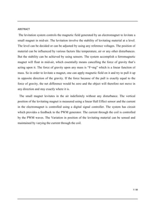
  • 1. 1/ 98 ABSTRACT The levitation system controls the magnetic field generated by an electromagnet to levitate a small magnet in mid-air. The levitation involve the stability of levitating material at a level. The level can be decided or can be adjusted by using any reference voltages. The position of material can be influenced by various factors like temperature, air or any other disturbances. But the stability can be achieved by using sensors. The system accomplish a ferromagnetic magnet will float in mid-air, which essentially means cancelling the force of gravity that’s acting upon it. The force of gravity upon any mass is “F=mg” which is a linear function of mass. So in order to levitate a magnet, one can apply magnetic field on it and try to pull it up in opposite direction of the gravity. If the force because of the pull is exactly equal to the force of gravity, the net difference would be zero and the object will therefore not move in any direction and stay exactly where it is. The small magnet levitates in the air indefinitely without any disturbance. The vertical position of the levitating magnet is measured using a linear Hall Effect sensor and the current in the electromagnet is controlled using a digital signal controller. The system has circuit which provides a feedback to the PWM generator. The current through the coil is controlled by the PWM waves. The Variation in position of the levitating material can be sensed and maintained by varying the current through the coil.
  • 2. P a g e | 2 CONTENTS Pag CHAPTER 1 INTRODUCTION 1.1 BASICS OF MAGNETIC LEVITATION 1.2 TYPES OF MAGNETS 1.3 DEFINITION OF MAGNETIC LEVITATION 1.3.1 Magnetic Levitation 1.3.2 Magnetic Suspension 1.3.3 Area of Attraction 1.3.4 Uses 1.3.5 Issues CHAPTER 2 BLOCK DIAGRAM OF PROJECT 2.1 CONTROLLER 2.2 COIL DRIVER 2.3 SOLENOID 2.4 HALL EFFECT SENSORS 2.5 FEEDBACK SYSTEMS 2.6 IR SENSOR CHAPTER 3 CIRCUIT DIAGRAM AND COMPONENTS USED 3.1 CIRCUIT DIAGRAM 3.2 WORKING 3.3 POWER SUPPLY 3.4 COMPONENTS DISCRIPTION 3.4.1 DIP (KA7500C): 3.4.2 DIFFERENTIAL AMPLIFIER Op -AMP 3.4.3 HALL EFFECT SENSORS
  • 3. P a g e | 3 3.4.4 MOSFET 3.4.4.1 Composition 3.4.4.2 Operation of Mosfet 3.4.5 VOLTAGE REGULATOR: 3.4.6 ELECROMAGNET 3.4.7 POTENTIOMETER 3.4.8 CAPACITORS 3.4.9 RESISTORS 3.4.10 DIODES 3.5 DATASHEETS CHAPTER 4 ADVANTAGES AND IMROVEMENTS CHAPTER 5 CONCLUSION AND FUTURE SCOPE REFFERENCES
  • 4. P a g e | 4 LIST OF FIGURES Fig. No Figures Name Page no Fig 1.1 Michael Faraday 3 Fig 1.2 Induced Current from Change in Magnetic Field 4 Fig 1.3 Heinrich Lenz 5 Fig 1.4 Perpendicular Force from Induce Current 6 Fig 1.5 Permanent Magnet Fields 7 Fig 1.6 Electromagnet 9 Fig 1.7 Magnetic levitation 10 Fig 1.8 Magnetic Suspension 11 Fig 1.9 Maglev Train 11 Fig 1.10 Contactless Melting 12 Fig 1.11 Magnetic Bearing 12 Fig 1.12 Product Display 13 Fig 2.1 Block Diagram 14 Fig 3.1 Circuit Diagram 18 Fig 3.2 DIP KA7500C 25 Fig 3.3 Pin diagram of KA7500C 26 Fig 3.4 Op-amp LM741 30 Fig 3.5 Pin out of LM741 30 Fig 3.6 Difference Amplifier. 31 Fig 3.7 Working of Op-amp on bread board 32 Fig 3.8 Hall sensor 33
  • 5. P a g e | 5 Fig 3.9 Working of hall effect sensors 34 Fig 3.10 Effect of magnets on the hall effect sensors. 36 Fig 3.11 MOSFET IRF540 40 Fig 3.12 Voltage Regulator 41 Fig 3.13 Industrial electromagnet lifting scrap iron 44 Fig 3.14 Electromagnets 46 Fig 3.15 Material levitating 46 Fig 3.16 Potentiometer 47 Fig 3.17 Diagramatic form of potentiometer 47 Fig 3.18 Single-turn potentiometer with metal casing removed to expose wiper contacts and resistive track 48 Fig 3.19 Paper capacitors 53 Fig 3.20 Ceramic Capacitors 54 Fig 3.21 Electrolytic capacitor 54 Fig 3.22 Symbol of resistors 55 Fig 3.23 Resistors 55 Fig 3.24 P-N junction diode 58 Fig 3.25 Schottky Diodes 59 Fig 3.26 Test Circuit 64 Fig 3.27 Operational Waveforms 65 CHAPTER 1 INTRODUCTION
  • 6. P a g e | 6 Some forces in this world are almost invisible to the naked eye and most people throughout the world do not even know they exist. On one side it can be said that some of these forces are abstract feelings inside of a human being that have been given names from man. These forces could be things like emotion, guilt, and even ecstasy. On the other side it have solid concrete principles determine how the world works. These too have been given names by man, but these principles are not abstract and have solid ground in science. These different principles are things like gravity, electricity, and magnetism. Magnetism has been a part of the earth since the beginning whether people realize it or not. It is due to the magnetism of the earth that the world spins and thus creates things like gravity. The magnetism is created by the processes within the core of the earth. The earth’s iron-ore core has a natural spinning motion to it inside which creates a natural magnetic force that is held constant over the earth. This creates magnetic forces that turn the earth into a large bar magnet. The creation of North and South poles on the earth are due to this field. From this magnetic field, things such as the aurora borealis can be seen that is a small electromagnetic storm in the atmosphere which creates a display for all to see. Not only does magnetism provide the world with amazing natural displays, but it also provides the world with amazing applications to society. One of these applications is magnetic levitation. Magnetic levitation uses the concept of a magnets natural repulsion to poles of the same kind. This repulsion has been harnessed and controlled in an environment to help create a system of transportation that is both economically sound and faster then most methods of transportation at this point. In 1965 the Department of Commerce established the High Speed Ground Transportation Act. Most early work on developing Maglev technology was developed during this time. The earliest work was carried out by the Brookhaven National Laboratory, Massachusetts Institute of Technology, Ford, Stanford Research Institute, Rohr Industries, Boeing Aerospace Co., and the Garrett Corporation. In the United States, though, the work ended in 1975 with the termination of Federal Funding for high-speed ground transportation and research. It was at that time when the Japanese and German developers continued their research and therefore came out with the first test tracks.
  • 7. P a g e | 7 1.1 BASICS OF MAGNETIC LEVITATION Magnetic Fields The creation of magnetic forces is the basis of all magnetic levitation. The creation of a magnetic field can be caused by a number of things. The first thing that it can be caused by is a permanent magnet. These magnets are a solid material in which there is an induced North and South pole. These will be described further a little later. The second way that a magnetic field can be created is through an electric field changing linearly with time. The third and final way to create a magnetic field is through the use of direct current. There are two basic principles in dealing with the concept of magnetic levitation. The first law that is applied was created by Michael Faraday. This is commonly known as Faraday’s Law. Fig 1.1 Michael Faraday
  • 8. P a g e | 8 This law states that if there is a change in the magnetic field on a coil of wire, there is seen a change in voltage. Taking that a bit further, it could be said that if there was a change in voltage, then there would be a change in magnetic field. This occurs in the coil when there is a current induced as a result of that change in voltage. From Figure 1.2 below it is illustrated that the change in the magnetic field produces a current. Fig 1.2 Induced Current from Change in Magnetic Field For the purposes of magnetic levitation the ability to change the strength of a magnetic field by just changing the current is powerful. If there is a need for more of a force, then sending more current through a coil of wires will produce more of a greater magnetic force. The direction of the forces created by Faraday’s Law was discovered by a man named Heinrich Lenz. His theory states that “the emf induced in an electric circuit always acts in such a direction that the current it drives around the circuit opposes the change in the magnetic flux which produces the emf.” In other words, this is stating that if there was a current that was created in a coil of wires, then the magnetic field that is being produced will be perpendicular the current direction.
  • 9. P a g e | 9 Fig 1.3 Heinrich Lenz The application that this has on magnetic levitation is that this will allow the direction of the magnetic field to be predictable and thus a set up can be created for a specific purpose to maximize the force that is created. This has direct application to the rail gun which will be described later.
  • 10. P a g e | 10 Fig 1.4 Perpendicular Force from Induce Current From Figure 1.4 above, it is illustrated that there is a coiled wire around the cylinder. Inside that coiled wire is a current that is traveling from left to right. The resulting magnetic force from that current is shown to be perpendicular to the current and is travelling from bottom to top. 1.2 TYPES OF MAGNETS Although the concepts of magnetic levitation are all the same, the way that those concepts are brought about can vary. These options are controlled and changed depending on the type of application that is necessary. Permanent Magnets The first type of levitation is the implementation through permanent magnets. These magnets are made of a material that creates a north and a south pole on them. This can be seen in Figure 1.5.
  • 11. P a g e | 11 Fig 1.5 Permanent Magnet Fields The formal definition of a permanent magnet is “a material that retains its magnetic properties after and external magnetic field is removed.” The whole idea behind permanent magnets is that like ends will repel and opposite ends will attract. Permanent magnets require very little if any maintenance. These magnets do not require cryogens or a large power supply for operation. The magnetic field is measured vertically within the bore of the magnet. The main disadvantages of a permanent magnet are the cost of the magnet itself when put into large scale systems. Another disadvantage is the varying changes in the magnetic field. The ability to control a constant magnetic force from a permanent magnet is an on-going problem in the application of these types of magnets. Different applications that use these types of magnets can be found in a number of different areas. Examples of these applications are compasses, DC motor drives, clocks, hearing aids, microphones, speedometers, and many more. Electromagnetic Magnets The basic idea behind an electromagnet is extremely simple. By running electric current through a wire, one can create a magnetic field. When this wire is coiled around a magnetic material (i.e. metal), a current is passed through this wire. In doing this, the electric current will magnetize the metallic core. This can be seen in Figure 1.6.
  • 12. P a g e | 12
  • 13. P a g e | 13 Fig 1.6 Electromagnet By using this simple principle, one can create all sorts of things including motors, solenoids, heads for hard disks, speakers, and so on. An electromagnet is one that uses the same type of principles as the permanent magnet but only on a temporary scale. This means that only when the current is flowing is there going to be an induced magnet. This type of magnet is an improvement to the permanent magnet because it allows somebody to select when and for how long the magnetic field lasts. It also gives a person control over how strong the magnet will be depending on the amount of current that is passed through the wire. Superconductive Magnets The ideas presented behind superconductive magnets are the same principles that are at work in an MRI. Superconductive magnets are the most common of all the magnets, and are sometimes called cryomagnets. The idea behind the superconducting magnets is that there is a material which presents no electrical resistivity to electrical current. Once a current has been fed into the coils of this material, it will indefinitely flow without requiring the input of any additional current. The way that a material is able to have such a low resistivity to current is that it is brought to very low temperatures. The temperatures that are commonly found in
  • 14. P a g e | 14 superconducting magnets are around -258*C. This is done by immersing the coils that are holding the current into liquid Helium; this also helps in maintaining a homogenous In 1990, legislative action directed the U.S. Army Corps of Engineers to implement and prepare a plan for a National Maglev program. The Department of Transportation (DOT), Department of Energy (DOE), and the Army Corp developed what is know as the National Maglev Initiative which was a two year 25 million dollar program to assess the engineering, economic, environmental and safety aspects of Maglev. 1.3 DEFINITION OF MAGNETIC LEVITATION Magnetic levitation, maglev or magnetic suspension is a method by which an object is suspended with no support other than magnetic fields. Magnetic force is used to counteract the effect of gravitational force. The Difference between levitation and suspension 1.3.1 Magnetic Levitation: If an object is kept in air using the force of repulsion given from the bottom of the object then it is known as magnetic levitation. Fig 1.7 Magnetic levitation 1.3.2 Magnetic Suspension: If a n object is suspended using the force of attraction applied from top of the object then it is known as magnetic suspension.
  • 15. P a g e | 15 Fig 1.8 Magnetic Suspension 1.3.3 Area of Attraction: The main area of attraction in the field of magnetic levitation is as a means of eliminating friction or physical contact. As a means of eliminating friction magnetic levitation gives its use in magnetic bearing. As a means of eliminating physical contact magnetic levitation gives its use in magnetic levitated trains. 1.3.4 Uses: Magnetic levitation finds its application in following applications: Maglev trains: For high speed ground transportation maglev trains are designed to take advantage of magnetic levitation. Fig 1.9 Maglev Train Contactless Melting: Metal having high resistance can be levitated and melt in magnetic field.
  • 16. P a g e | 16 Fig 1.10 Contactless Melting Magnetic Bearing: For rotating machines to stabilize shaft without friction and contact magnetic bearing are used. Fig 1.11 Magnetic Bearing Product Display Purpose: For displaying the product by levitating it in air.
  • 17. P a g e | 17 Fig 1.12 Product Display 1.3.5 Issues Primary issues involved in magnetic levitation are stability and lifting force. Lifting force should be sufficient to provide upward force to counteract gravity. Stability to ensure that the system does not slide or flip into a configuration when lift is neutralized CHAPTER 2 BLOCK DIAGRAM OF PROJECT
  • 18. P a g e | 18 Fig 2.1 Block Diagram The block diagram of levitation system have 5 blocks. Each block have its own advantage and necessary for project. Functions of various blocks can be overviewed as follows : 2.1 CONTROLLER Controller will be the heart of the project. It helps in controlling the current travelling through the coil. Controller can be any PWM generator. Here KA7500C is being used .
  • 19. P a g e | 19 2.2 COIL DRIVER Coil driver can be a MOSFET which is used as switching device. Coil driver is used for driving current through coil. 2.3 SOLENOID Coil bounded over a metal core forming a solenoid is used as electromagnet which produces magnetic field when current is passed through it. 2.4 HALL EFFECT SENSORS Sensors are used to sense the variation in the level of levitating material and provides a ray data to the feedback system which compares the raw data in the form of voltages with the reference provided by the controller and hence forms a closed loop system. 2.5 FEEDBACK SYSTEMS Feedback systems involves input from hall sensors, comparing the hall voltages with the reference voltages and providing the signal amplification, compensation etc. These signals from the feedback unit thus help in controlling the duty cycle of PWM waves generated by generator which in turns control the current driven through coil and thus control the magnetic field through coil. The levitating material can be any magnet which is suspended at a level. The circuit diagram , the components used , the working of each components, can be explained in detail in next chapters. 2.6 IR SENSOR The IR sensors are used to set a limit for the levitating object beyond which if the object moves toward the electromagnet the power supply to the electromagnet is cut for a small time and eventually when the object falls back below the limit, the supply is restored .This prevents the object from getting sucked into the electromagnet.
  • 20. P a g e | 20
  • 21. P a g e | 21 CHAPTER 3 CIRCUIT DIAGRAM AND COMPONENTS USED 3.1 CIRCUIT DIAGRAM
  • 22. P a g e | 22 Fig 3.1Circuit Diagram  DIP (KA74500C)
  • 23. P a g e | 23  O-amp (LM741)  Voltage Regulator  Hall Effect Sensor  Electromagnet  MOSFET  Potentiometer  Diode  Resistors  Capacitor Above are the components used in circuit of magnetic levitation System. KA7500C DIP, O-amp LM741, Voltage regulator, Hall effect sensors, Electromagnets, MOSFET, potentiometer, Diodes, Resistor, Capacitors are the components. Each component is fixed on PCB and the soldering is done with the help of soldering rod Whole circuit will work on 5-12V DC supply, a full wave rectifier is used to rectify the AC supply which is then filtered by the electrolytic Capacitors. Voltage regulators are used to regulate the supply to the circuit. Each component is described in the next chapters.
  • 24. P a g e | 24 3.2 WORKING The system accomplish that an ferromagnetic substance will float in mid-air, which essentially means cancelling the force of gravity that’s acting upon it. The force of gravity upon any mass is “F=mg” which is a linear function of mass. Now, if the item that one have to float or levitate is ferromagnetic, one can apply magnetic field on it and try to pull it up in opposite direction of the gravity .If the force because of the pull is exactly equal to the force of gravity, the net difference would be zero and the object will therefore not move in any direction and stay exactly where it is. It’s pretty complicated to do. As the force acting on the object is not a linear function but is a function of the square of the distance. Therefore, as the object get’s closer to the source of magnetic field, the strength of the force increases by square and it gets sucked right into it. So in order to create a magnetic field that one can control the current is pushed through a coil with ferromagnetic centre at the middle and magnetic field was generated. Now, it is needed to somehow measure the distance between the object and the magnetic field being generated and use this distance to correct the amount of current that we have to apply which essentially forms a feedback loop, as error value of the distance is used to correct magnetic field. Say, if object gets really close to magnet ,then one can sense the distance ,measure that and feed that back and reduce the strength of magnetic field so that the object can fall back down . On the other hand If the object is falling back too much and one detect that it is too far from the magnet and then strengthen the magnetic field to bring the object back up. So this negative feedback system can be used in order to keep this object in middle and not allow it to move up and down, so that it can hover at a specific location by precisely matching the two forces. In order to find out the position of object in free space and for measurement of distance Hall effect sensor are used. The Hall effect itself was discovered by Edwin Hall in 1879, when he discovered that it is possible for current to be effected by magnetic field in a conductor. The modern Hall effect sensors make use of semiconductor and give us the strength of magnetic going through it. So essentially the semiconductor inside is effected by the magnetic field. The Hall effect sensor used gives an voltage at the output. It gives an analog voltage output that is proportional to the strength of the magnetic field (as we are making an analog circuit).Here two
  • 25. P a g e | 25 magnetic fields is in action ,one is the magnetic field generated by the magnet at the top and the other is by the object trying to hover at the bottom. A Hall effect sensor is placed on the lower edge of the electromagnet. The two magnetic fields interact together where the Hall effect sensor is and they add the magnetic fields. The magnetic field from the electromagnet is same but there is a variation in the net magnetic field because of the movement of the object. Therefore the total magnetic field that passes through the Hall effect sensor becomes direct function of the location of the magnet itself. So if the object is moved close to the Hall probe, the strength of the magnetic field through the Hall effect sensor is strong and so the output of the Hall effect sensor will tell us that the magnetic field is really strong and therefore the object must be really close to the sensor and the magnetic field weakens going through the Hall effect sensor as seen by its output which drops. Here two Hall effect sensors are used , one sitting at the top of the electromagnet and the other at the bottom of the electromagnet and by subtracting the voltages between the two Hall effect sensors ,one can isolate only the effect of the magnet at the bottom . So measure of the location of the object had been made . As the magnetic field going through the Hall effect sensor at the top is only the magnetic field produced by the electromagnet and the magnetic field through the lower sensor is the combined effect of the magnetic field of the electromagnet and the hovering magnet. So, by subtracting the two output voltages one can get the voltage that is proportional to the distance of the magnet that one is trying to hover. Now the voltage that is needed to control the amount of current that goes through the magnet that creates the magnetic field . The IC will take the output voltage from Hall effect’s and control the current through the inductor itself. There were many ways of taking the output of the Hall effect sensor. One could directly digitized the output that comes from the Hall effect sensor and used a microcontroller and by programming the microcontroller with the feedback parameters that have controlled the current through the inductor. That would be totally a digital way of doing it, that would require a software and use of microcontroller, but one need to do it with the actual component’s itself . The entirely opposite that would be using an entirely analog means i.e building an analog difference amplifier and taking the error voltage and amplifying it and passing it through proper control circuitary and
  • 26. P a g e | 26 the controlling the current through the inductor. That would be another extreme which takes all analog means. But somewhere in middle, it is wanted to use Pulse Width Modulation to control the current that goes through the inductor . It is wanted to turn the current source (I) ON and OFF really quickly as opposed to have an analog voltage that controls it. So KA7500C IC from Fairchild semiconductors is being used. It is an IC intended to use in dc-dc converters and is essentially a PWM Controller. It has a PWM Controller and Error Amplifiers build into it, which was perfect as an error amplifier that controls the PWM which will control the current through the inductor that would adjust the magnetic field. The IC has an oscillator, which can give it a resistor and capacitor in order to set the RC time constant of the oscillator and get the oscillation frequency that one is looking for. That would be the PWM frequency that would come out of the IC. Frequency of 2KHzis used and it can be used upto 300KHz. The capacitor will create a ramp oscillations and this ramp is then feed directly into the PWM comparator. Now one side of the PWM comparator is the ramp voltage and the other side of the PWM comparator is the output of the error amplifier’s. So if the error is all the way positive means that the error amplifiers sense the error too large that V(+) is very higher than V(-). The output will become high and the PWM Comparator will give us a ‘1’ and that will be 100% duty cycle . If the output of the error amplifiers is low then the comparator will always give ‘0’ meaning 0% duty cycle. These are the two extremes of the duty cycle and anything in middle will give duty cycle at the output that is proportional to the error function feed inside it. The output at the emitter of the PWM Controller is feedback to control the error voltage to the error amplifier and can adjust the duty cycle to give the exact voltage that one want at the output. The difference between voltage from Hall effect sensors is taken through the operational amplifier. The op-amp is used in differential mode as all the resistances acting upon it are equal. The output from the op-amp will give the difference between the two voltages from the Hall effect sensors and this will be the feedback voltage which will be proportional to the position of magnet with respect to the edge of the electromagnet. The voltage is directly proportional to the distance between the object and the electromagnet. If distance between them is less voltage at output will be low and if the distance between them is large then the voltage at the corresponding output will be high. In order to adjust the distance one want to achieve, reference is set. For
  • 27. P a g e | 27 setting up a reference voltage a potentiometer is used. So once the two voltages to the error amplifiers are same the error will be zero and the magnetic levitation has been said to be achieved. The output from the PWM is taken from emitters and directly connected to a high voltage MOSFET, which then turns the electromagnet ON and OFF really quickly. A resistor is added to the electromagnet to limit the current in the electromagnet. If all the current was to pass through the electromagnet it will overwarm and will saturate the Hall effect sensors thus destroying them as very sensitive Hall effect sensors is being used. A diode in reverse polarity is also connected directly across the electromagnet. As the current was turning ON and OFF in the electromagnet when a PWM is applied to it. Every time the current is turned OFF a voltage is generated across the inductor because of its property to induce a negative voltage when a varying current is applied to it. As the back emf through the inductor depends on the rate of change of current through it and as this rate is high so a large back emf will be induced and this emf can damage the transistor which is being used as a switch in this circuit. So to counter the back emf induced because of varying current a free-wheeling diode is used across the inductor. This diode will absorb the reverse voltage across the inductor thus preventing damage to the transistor. 3.3 POWER SUPPLY A regulated ac power is input from the 220V mains and is converted into a 12-15V ac and a 5V dc supply. The 12V ac is required by the electromagnet and the 5V dc is required for the internal circuit to work . For converting the high input ac to a regulated ac or dc step down transformer along with rectifier is used . The main is connected to the input of the transformer at primary and the secondary is used for regulated output power. The electromagnet requires 1.2Amp current for functioning .Voltage regulator provides the regulated output to the circuit.
  • 28. P a g e | 28 3.4 COMPONENTS DISCRIPTION The description of various components used in the circuit is given below. 3.4.1 DIP (KA7500C) The KA7500C is used for the control circuit of the pulse width modulation switching regulator. The KA7500C consists of 5V reference voltage circuit, two error amplifiers, flip flop, an output control circuit, a PWM comparator, a dead time comparator and an oscillator. This device can be operated in the switching frequency of 1kHz to 300kHz. The precision of voltage reference (Vref) is improved up to ±1% with trimming. This provides a better output voltage regulation. The operating temperature range is -25°C ~ +85°C.
  • 29. P a g e | 29 Fig 3.2 DIP KA7500C FEATURES:- • Complete PWM Power Control Circuitry • Uncommitted Outputs for 200mA Sink or Source Current • Output Control Selects Single-Ended or Push-Pull Operation • Internal Circuitry Prohibits Double Pulse at Either Output • Variable Dead-Time Provides Control over Total Range • Internal Regulator Provides a Stable 5-V Reference Supply • Circuit Architecture Allows Easy Synchronization
  • 30. P a g e | 30 PIN DIAGRAM:- Fig 3.3 Pin diagram of KA7500C It is an IC intended for use in DC-DC conversions .It has an PWM controller and it has error amplifier built into it which is required in the project. The error amplifier controls the PWM which in turns control the current through the inductor that adjusts the magnetic field. In the oscillator part it is needed to connect a capacitor and a resistor which will decide the RC time constant of the oscillator and get the oscillating frequency so that it would be the PWM frequency that would comeout of the IC. Here it is using 2KHz but it can be used all the way up to 300KHz. Because of the presence of capacitor Ramp voltage is generated and this ramp is feed to the one side of the comparator and the other side of the comparator is the output of the error amplifiers .Looking into the open loop If the error is high that is error is more positive ,then the output of the error amplifiers is high then the comparator will always give a 1 that is 100% duty cycle .On the other hand if the output is more low that is negative ,then the output will be low and the comparator will always give out a 0 that is 0% duty cycle .So these are the two extremes of the duty cycle and anything in the middle will be proportional to the error function feed to the error amplifiers. At the output of pin 8 if one apply source voltage at pin 8 and connect a resistor at the pin 9 it is seen that a PWM wave is generated at the output with pulse width directly
  • 31. P a g e | 31 proportional to the error voltage feed. So its this PWM which is used to counter the error and hence try to levitate the magnet using a Reference voltage. 3.4.2 DIFFERENTIAL AMPLIFIER Op-AMP A differential amplifier is a type of electronic amplifier that amplifies the difference between two input voltages but suppresses any voltage common to the two inputs. It is an analog circuit with two inputs and and one output in which the output is ideally proportional to the difference between the two voltages Where A is the gain of amplifier. Many electronic devices use differential amplifiers internally. The output of an ideal differential amplifier is given by: Where and are the input voltages and is the differential gain. In practice, however, the gain is not quite equal for the two inputs. This means, for instance, that if and are equal, the output will not be zero, as it would be in the ideal case. A more realistic expression for the output of a differential amplifier thus includes a second term. Is called the common-mode gain of the amplifier.
  • 32. P a g e | 32 As differential amplifiers are often used to null out noise or bias-voltages that appear at both inputs, a low common-mode gain is usually desired. The common-mode rejection ratio (CMRR), usually defined as the ratio between differential- mode gain and common-mode gain, indicates the ability of the amplifier to accurately cancel voltages that are common to both inputs. The common-mode rejection ratio is defined as: In a perfectly symmetrical differential amplifier, is zero and the CMRR is infinite. Note that a differential amplifier is a more general form of amplifier than one with a single input; by grounding one input of a differential amplifier, a single-ended amplifier results. Operational Modes To explain the circuit operation, four particular modes are isolated below although, in practice, some of them act simultaneously and their effects are superimposed. Biasing In contrast with classic amplifying stages that are biased from the side of the base (and so they are highly β-dependent), the differential pair is directly biased from the side of the emitters by sinking/injecting the total quiescent current. The series negative feedback (the emitter degeneration) makes the transistors act as voltage stabilizers; it forces them to adjust their VBE voltages (base currents) to pass the quiescent current through their collector-emitter junctions. So, due to the negative feedback, the quiescent current depends only slightly on the transistor's β. The biasing base currents needed to evoke the quiescent collector currents usually come from the ground, pass through the input sources and enter the bases. So, the sources have to be galvanic (DC) to ensure paths for the biasing current and low resistive enough to not create significant voltage drops across them. Otherwise, additional DC elements should be connected between the bases and the ground (or the positive power supply).
  • 33. P a g e | 33 Common mode At common mode (the two input voltages change in the same directions), the two voltage (emitter) followers cooperate with each other working together on the common high-resistive emitter load (the "long tail"). They all together increase or decrease the voltage of the common emitter point (figuratively speaking, they together "pull up" or "pull down" it so that it moves). In addition, the dynamic load "helps" them by changing its instant ohmic resistance in the same direction as the input voltages (it increases when the voltage increases and vice versa.) thus keeping up constant total resistance between the two supply rails. There is a full (100%) negative feedback; the two input base voltages and the emitter voltage change simultaneously while the collector currents and the total current do not change. As a result, the output collector voltages do not change as well. Differential mode Normal. At differential mode (the two input voltages change in opposite directions), the two voltage (emitter) followers oppose each other - while one of them tries to increase the voltage of the common emitter point, the other tries to decrease it (figuratively speaking, one of them "pulls up" the common point while the other "pulls down" it so that it stays immovable) and v.v. So, the common point does not change its voltage; it behaves like a virtual ground with a magnitude determined by the common-mode input voltages. The high-resistive emitter element does not play any role since it is shunted by the other low-resistive emitter follower. There is no negative feedback since the emitter voltage does not change at all when the input base voltages change. Тhe common quiescent current vigorously steers between the two transistors and the output collector voltages vigorously change. The two transistors mutually ground their emitters; so, although they are common-collector stages, they actually act as common-emitter stages with maximum gain. Bias stability and independence from variations in device parameters can be improved by negative feedback introduced via cathode/emitter resistors with relatively small resistances. Overdriven. If the input differential voltage changes significantly (more than about a hundred millivolts), the transistor driven by the lower input voltage turns off and its collector voltage reaches the positive supply rail. At high overdrive the base-emitter junction gets reversed. The
  • 34. P a g e | 34 other transistor (driven by the higher input voltage) drives all the current. If the resistor at the collector is relatively large, the transistor will saturate. With relatively small collector resistor and moderate overdrive, the emitter can still follow the input signal without saturation. This mode is used in differential switches and ECL gates. Breakdown. If the input voltage continues increasing and exceeds the base-emitter breakdown voltage, the base-emitter junction of the transistor driven by the lower input voltage breaks down. If the input sources are low resistive, an unlimited current will flow directly through the "diode bridge" between the two input sources and will damage them. At common mode, the emitter voltage follows the input voltage variations; there is a full negative feedback and the gain is minimum. At differential mode, the emitter voltage is fixed (equal to the instant common input voltage); there is no negative feedback and the gain is maximum. Operational amplifier LM741 as differential amplifier An operational amplifier, or op-amp, is a differential amplifier with very high differential-mode gain, very high input impedance, and low output impedance. By applying negative feedback, an op-amp differential amplifier with predictable and stable gain can be built. Some kinds of differential amplifier usually include several simpler differential amplifiers. For example, a fully differential amplifier, an instrumentation amplifier, or an isolation amplifier are often built from several op-amps Fig 3.4 Op-amp LM741 Fig 3.5 Pin out of LM741 By connecting one voltage signal from one hall effect sensor onto one input terminal and another voltage signal from the other hall effect sensor onto the other input terminal the resultant output
  • 35. P a g e | 35 voltage will be proportional to the “Difference” between the two input voltage signals of V1 and V2. Then differential amplifier amplify the difference between two voltages making this type of operational amplifier circuit a subtractor. The output of the difference amplifier is the error voltage which is feed to the controller for controlling the width of the Pulse width wave generated. Fig 3.6 Difference Amplifier. Here, When R1=R2=R3=R4 the circuit becomes a Unity Gain Differential Amplifier and its output can be calculated from the expression So as R3=R1=10KOhm Hence the output of the differential amplifier is given as Vout = V2 - V1 This helps in calculating the error. If the suspended magnet is completely levitating then the output of the differentiator will be ZERO .Otherwise there will be a positive error is the magnet is too close to the electromagnet or the error will be negative if it is falling apart the electromagnet.
  • 36. P a g e | 36 Fig 3.7 Working of Op-amp on bread board 3.4.3 HALL EFFECT SENSORS A Hall effect sensor is a transducer that varies its output voltage in response to a magnetic field. Hall effect sensors are used for proximity switching, positioning, speed detection, and current sensing applications. In its simplest form, the sensor operates as an analog transducer, directly returning a voltage. With a known magnetic field, its distance from the Hall plate can be determined. Using groups of sensors, the relative position of the magnet can be deduced. Frequently, a Hall sensor is combined with circuitry that allows the device to act in a digital (on/off) mode, and may be called a switch in this configuration. Commonly seen in industrial applications such as the pictured pneumatic cylinder, they are also used in consumer equipment; for example some computer printers use them to detect missing paper and open covers. When high reliability is required, they are used in keyboards. Hall sensors are commonly used to time the speed of wheels and shafts, such as for internal combustion engine ignition timing, tachometers and anti-lock braking systems. They are used in brushless DC electric motors to detect the position of the permanent magnet. In the pictured
  • 37. P a g e | 37 wheel with two equally spaced magnets, the voltage from the sensor will peak twice for each revolution. This arrangement is commonly used to regulate the speed of disk drives Fig 3.8 Hall sensor Hall probe A Hall probe contains an indium compound semiconductor crystal such as indium antimonide, mounted on an aluminum backing plate, and encapsulated in the probe head. The plane of the crystal is perpendicular to the probe handle. Connecting leads from the crystal are brought down through the handle to the circuit box. When the Hall probe is held so that the magnetic field lines are passing at right angles through the sensor of the probe, the meter gives a reading of the value of magnetic flux density (B). A current is passed through the crystal which, when placed in a magnetic field has a "Hall effect" voltage developed across it. The Hall effect is seen when a conductor is passed through a uniform magnetic field. The natural electron drift of the charge carriers causes the magnetic field to apply a Lorentz force (the force exerted on a charged particle in an electromagnetic field) to these charge carriers. The result is what is seen as a charge separation, with a buildup of either positive or negative charges on the bottom or on the top of the plate. The crystal measures 5 mm square. The probe handle, being made of a non-ferrous material, has no disturbing effect on the field. A Hall probe should be calibrated against a known value of magnetic field strength. For a solenoid the Hall probe is placed in the center.
  • 38. P a g e | 38 Working principle When a beam of charged particles passes through a magnetic field, forces act on the particles and the beam is deflected from a straight path. The flow of electrons through a conductor is known as a beam of charged carriers. When a conductor is placed in a magnetic field perpendicular to the direction of the electrons, they will be deflected from a straight path. As a consequence, one plane of the conductor will become negatively charged and the opposite side will become positively charged. The voltage between these planes is called Hall voltage. When the force on the charged particles from the electric field balances the force produced by magnetic field, the separation of them will stop. If the current is not changing, then the Hall voltage is a measure of the magnetic flux density. Basically, there are two kinds of Hall effect sensors. One is linear which means the output of voltage linearly depends on magnetic flux density; the other is called threshold which means there will be a sharp decrease of output voltage at each magnetic flux density. Fig 3.9 Working of hall effect sensors Materials for Hall effect sensors The key factor determining sensitivity of Hall effect sensors is high electron mobility. As a result, following materials are especially suitable for Hall effect sensors:  Gallium arsenide (GaAs)  Indium arsenide (InAs)  Indium phosphide (InP)
  • 39. P a g e | 39  Indium antimonide (InSb)  Graphene Signal processing and interface Hall effect sensors are linear transducers. As a result, such sensors require a linear circuit for processing of the sensor's output signal. Such a linear circuit:  Provides a constant driving current to the sensors  Amplifies the output signal In some cases the linear circuit may cancel the offset voltage of Hall effect sensors. Moreover, AC modulation of the driving current may also reduce the influence of this offset voltage. Hall effect sensors with linear transducers are commonly integrated with digital electronics. This enables advanced corrections of the sensor's characteristics (e.g. temperature coefficient corrections) and digital interfacing to microprocessor systems. In some solutions of IC Hall effect sensors a DSP is used, which provides for more choices among processing techniques. The Hall effect sensor interfaces may include input diagnostics, fault protection for transient conditions, and short/open circuit detection. It may also provide and monitor the current to the Hall effect sensor itself. There are precision IC products available to handle these features. Advantages A Hall effect sensor may operate as an electronic switch.  Such a switch costs less than a mechanical switch and is much more reliable.  It can be operated up to 100 kHz.  It does not suffer from contact bounce because a solid state switch with hysteresis is used rather than a mechanical contact.  It will not be affected by environmental contaminants since the sensor is in a sealed package. Therefore, it can be used under severe conditions.  In the case of linear sensor (for the magnetic field strength measurements), a Hall effect sensor:  can measure a wide range of magnetic fields  is available that can measure either North or South pole magnetic Fields.
  • 40. P a g e | 40 Fig 3.10 Effect of magnets on the hall effect sensors. Disadvantages Hall effect sensors provide much lower measuring accuracy than fluxgate magnetometers or magneto resistance-based sensors. Moreover, Hall effect sensors drift significantly, requiring compensation. Applications 1. Position sensing Sensing the presence of magnetic objects (connected with the position sensing) is the most common industrial application of Hall effect sensors, especially those operating in the switch mode (on/off mode). The Hall effect sensors are also used in the brushless DC motor to sense the position of the rotor and to switch the transistors in the right sequence. Smartphones use hall sensors to determine if the Flip Cover accessory is closed. 2. Direct Current (DC) transformers Hall effect sensors may be utilized for contactless measurements of DC current in current transformers. In such a case the Hall effect sensor is mounted in the gap in magnetic core around the current conductor. As a result, the DC magnetic flux can be measured, and the DC current in the conductor can be calculated. 3. Automotive fuel level indicator
  • 41. P a g e | 41 The Hall sensor is used in some automotive fuel level indicators. The main principle of operation of such indicator is position sensing of a floating element. This can either be done by using a vertical float magnet or a rotating lever sensor.  In a vertical float system a permanent magnet is mounted on the surface of a floating object. The current carrying conductor is fixed on the top of the tank lining up with the magnet. When the level of fuel rises, an increasing magnetic field is applied on the current resulting in higher Hall voltage. As the fuel level decreases, the Hall voltage will also decrease. The fuel level is indicated and displayed by proper signal condition of Hall voltage.  In a rotating lever sensor a diametrically magnetized ring magnet rotates about a linear hall sensor. The sensor only measures the perpendicular (vertical) component of the field. The strength of the field measured correlates directly to the angle of the lever and thus the level of the fuel tank. 4. Keyboard Switch Developed by Everett A. Vorthmann and Joseph T. Maupin for Micro Switch (a division of Honeywell) in 1969, the switch was known to still be in production until as late as 1990. The switch is one of the highest quality keyboard switches ever produced, with reliability being the main aim of the design. The key-switches have been tested to have a lifetime of over 30 billion key presses, the switch also has dual open-collector outputs for reliability. The Honeywell Hall Effect switch is most famous used in the Space-cadet keyboard, a keyboard used on LISP machines. 3.4.4 MOSFET The metal–oxide–semiconductor field-effect transistor (MOSFET, MOS-FET, or MOS FET) is a type of transistor used for amplifying or switching electronic signals. Although the MOSFET is a four-terminal device with source (S), gate (G), drain (D), and body (B) terminals, the body (or substrate) of the MOSFET is often connected to the source terminal, making it a three-terminal device like other field-effect transistors. Because these two terminals are normally connected to each other (short-circuited) internally, only three terminals appear in
  • 42. P a g e | 42 electrical diagrams. The MOSFET is by far the most common transistor in both digital and analog circuits, though the bipolar junction transistor was at one time much more common. The main advantage of a MOSFET over a regular transistor is that it requires very little current to turn on (less than 1mA), while delivering a much higher current to a load (10 to 50A or more). In enhancement mode MOSFETs, a voltage drop across the oxide induces a conducting channel between the source and drain contacts via the field effect. The term "enhancement mode" refers to the increase of conductivity with increase in oxide field that adds carriers to the channel, also referred to as the inversion layer. The channel can contain electrons (called an nMOSFET or nMOS), or holes (called a pMOSFET or pMOS), opposite in type to the substrate, so nMOS is made with a p-type substrate, and pMOS with an n-type substrate (see article on semiconductor devices). In the less common depletion mode MOSFET, detailed later on, the channel consists of carriers in a surface impurity layer of opposite type to the substrate, and conductivity is decreased by application of a field that depletes carriers from this surface layer. 3.4.4.1 Composition Usually the semiconductor of choice is silicon, but some chip manufacturers, most notably IBM and Intel, recently started using a chemical compound of silicon and germanium (SiGe) in MOSFET channels. Unfortunately, many semiconductors with better electrical properties than silicon, such as gallium arsenide, do not form good semiconductor-to-insulator interfaces, and thus are not suitable for MOSFETs. Research continues on creating insulators with acceptable electrical characteristics on other semiconductor material. In order to overcome the increase in power consumption due to gate current leakage, a high-κ dielectric is used instead of silicon dioxide for the gate insulator, while polysilicon is replaced by metal gates (see Intel announcement). The gate is separated from the channel by a thin insulating layer, traditionally of silicon dioxide and later of silicon oxynitride. Some companies have started to introduce a high-κ dielectric + metal gate combination in the 45 nanometer node. When a voltage is applied between the gate and body terminals, the electric field generated penetrates through the oxide and creates an "inversion layer" or "channel" at the semiconductor-
  • 43. P a g e | 43 insulator interface. The inversion channel is of the same type, p-type or n-type, as the source and drain, and thus it provides a channel through which current can pass. Varying the voltage between the gate and body modulates the conductivity of this layer and thereby controls the current flow between drain and source. This is known as enhancement mode. 3.4.4.2 Operation of Mosfet The traditional metal–oxide–semiconductor (MOS) structure is obtained by growing a layer of silicon dioxide (SiO2) on top of a silicon substrate and depositing a layer of metal or polycrystalline silicon (the latter is commonly used). As the silicon dioxide is a dielectric material, its structure is equivalent to a planar capacitor, with one of the electrodes replaced by a semiconductor. When a voltage is applied across a MOS structure, it modifies the distribution of charges in the semiconductor. If we consider a p-type semiconductor a positive voltage, from gate to body (see figure) creates a depletion layer by forcing the positively charged holes away from the gate- insulator/semiconductor interface, leaving exposed a carrier-free region of immobile, negatively charged acceptor ions . IF is high enough, a high concentration of negative charge carriers forms in an inversion layer located in a thin layer next to the interface between the semiconductor and the insulator. Unlike the MOSFET, where the inversion layer electrons are supplied rapidly from the source/drain electrodes, in the MOS capacitor they are produced much more slowly by thermal generation through carrier generation and recombination centres in the depletion region. Conventionally, the gate voltage at which the volume density of electrons in the inversion layer is the same as the volume density of holes in the body is called the threshold voltage. When the voltage between transistor gate and source (VGS) exceeds the threshold voltage (Vth), it is known as overdrive voltage. This structure with p-type body is the basis of the n-type MOSFET, which requires the addition of an n-type source and drain regions. Here, MOSFET IRF540 is used
  • 44. P a g e | 44 Fig 3.11 MOSFET IRF540 MOSFET IRF540 This MOSFET series realized with STMicroelectronics unique Strip FET process has specifically been designed to minimize input capacitance and gate charge. It is therefore suitable as primary switch in advanced high efficiency, high-frequency isolated DC-DC converters for Telecom and Computer applications. It is also intended for any applications with low gate drive requirements. It has   EXCEPTIONAL dv/dt CAPABILITY  100% AVALANCHE TESTED  LOW GATE CHARGE  APPLICATION ORIENTED  CHARACTERIZATION APPLICATIONS  HIGH-EFFICIENCY DC-DC CONVERTERS  UPS AND MOTOR CONTROL
  • 45. P a g e | 45 3.4.5 VOLTAGE REGULATOR: A voltage regulator generates a fixed output voltage of a preset magnitude that remains constant regardless of changes to its input voltage or load conditions. There are two types of voltage regulators: linear and switching. A linear regulator employs an active (BJT or MOSFET) pass device (series or shunt) controlled by a high gain differential amplifier. It compares the output voltage with a precise reference voltage and adjusts the pass device to maintain a constant output voltage. A switching regulator converts the dc input voltage to a switched voltage applied to a power MOSFET or BJT switch. The filtered power switch output voltage is fed back to a circuit that controls the power switch on and off times so that the output voltage remains constant regardless of input voltage or load current changes. Switching regulators require a means to vary their output voltage in response to input and output voltage changes. One approach is to use PWM that controls the input to the associated power switch, which controls its on and off time (duty cycle). In operation, the regulator's filtered output voltage is fed back to the PWM controller to control the duty cycle. If the filtered output tends to change, the feedback applied to the PWM controller varies the duty cycle to maintain a constant output voltage. Fig 3.12 Voltage Regulator A voltage regulator is designed to automatically maintain a constant voltage level. A voltage regulator may be a simple "feed-forward" design or may include negative feedback control loops.
  • 46. P a g e | 46 It may use an electromechanical mechanism, or electronic components. Depending on the design, it may be used to regulate one or more AC or DC voltages. Electronic voltage regulators are found in devices such as computer power supplies where they stabilize the DC voltages used by the processor and other elements. In automobile alternators and central power station generator plants, voltage regulators control the output of the plant. In an electric power distribution system, voltage regulators may be installed at a substation or along distribution lines so that all customers receive steady voltage independent of how much power is drawn from the line. Voltage regulators or stabilizers are used to compensate for voltage fluctuations in mains power. Large regulators may be permanently installed on distribution lines. Small portable regulators may be plugged in between sensitive equipment and a wall outlet. Automatic voltage regulators are used on generator sets on ships, in emergency power supplies, on oil rigs, etc. to stabilize fluctuations in power demand. For example, when a large machine is turned on, the demand for power is suddenly a lot higher. The voltage regulator compensates for the change in load. Commercial voltage regulators normally operate on a range of voltages, for example 150–240 V or 90–280 V. Servo stabilizers are also manufactured and used widely in spite of the fact that they are obsolete and use out-dated technology. Voltage regulators are used in devices like air conditioners, refrigerators, televisions etc. in order to protect them from fluctuating input voltage. The major problem faced is the use of relays in voltage regulators. Relays create sparks which result in faults in the product. Many simple DC power supplies regulate the voltage using either series or shunt regulators, but most apply a voltage reference using a shunt regulator such as a Zener diode, avalanche breakdown diode, or voltage regulator tube. Each of these devices begins conducting at a specified voltage and will conduct as much current as required to hold its terminal voltage to that specified voltage by diverting excess current from a non-ideal power source to ground, often through a relatively low-value resistor to dissipate the excess energy. The power supply is designed to only supply a maximum amount of current that is within the safe operating capability of the shunt regulating device.
  • 47. P a g e | 47 If the stabilizer must provide more power, the shunt regulator output is only used to provide the standard voltage reference for the electronic device, known as the voltage stabilizer. The voltage stabilizer is the electronic device, able to deliver much larger currents on demand. Here the voltage regulators are used to provide a regulated supply to the circuit. A constant voltage is provided and hence it work as a voltage stabilizer. Voltage stabilizer is used to stabilize the input voltage to a required level. 3.4.6 ELECROMAGNET An electromagnet is a type of magnet in which the magnetic field is produced by an electric current. The magnetic field disappears when the current is turned off. Electromagnets usually consist of a large number of closely spaced turns of wire that create the magnetic field. The wire turns are often wound around a magnetic core made from a ferromagnetic or ferrimagnetic material such as iron; the magnetic core concentrates the magnetic flux and makes a more powerful magnet. The main advantage of an electromagnet over a permanent magnet is that the magnetic field can be quickly changed by controlling the amount of electric current in the winding. However, unlike a permanent magnet that needs no power, an electromagnet requires a continuous supply of current to maintain the magnetic field. Electromagnets are widely used as components of other electrical devices, such as motors, generators, relays, loudspeakers, hard discs, MRI machines, scientific instruments, and magnetic separation equipment. Electromagnets are also employed in industry for picking up and moving heavy iron objects such as scrap iron and steel. Uses of electromagnets
  • 48. P a g e | 48 Fig 3.13 Industrial electromagnet lifting scrap iron A portative electromagnet is one designed to just hold material in place; an example is a lifting magnet. A tractive electromagnet applies a force and moves something. Electromagnets are very widely used in electric and electromechanical devices, including:  Motors and generators  Transformers  Relays, including reed relays originally used in telephone exchanges  Electric bells and buzzers  Loudspeakers and earphones  Actuators  Magnetic recording and data storage equipment: tape recorders, VCRs, hard disks  MRI machines  Scientific equipment such as mass spectrometers  Particle accelerators  Magnetic locks
  • 49. P a g e | 49  Magnetic separation equipment, used for separating magnetic from nonmagnetic material, for example separating ferrous metal from other material in scrap.  Industrial lifting magnets  magnetic levitation  Induction heating for cooking, manufacturing, and hyperthermia therapy Electromagnets for Magnetic Levitation  A conductor can be levitated above an electromagnet (or vice versa) with an alternating current flowing through it. This causes any regular conductor to behave like a diamagnet, due to the eddy currents generated in the conductor. Since the eddy currents create their own fields which oppose the magnetic field, the conductive object is repelled from the electromagnet, and most of the field lines of the magnetic field will no longer penetrate the conductive object.  This effect requires non-ferromagnetic but highly conductive materials like aluminium or copper, as the ferromagnetic ones are also strongly attracted to the electromagnet (although at high frequencies the field can still be expelled) and tend to have a higher resistivity giving lower eddy currents. Again, lifts wire gives the best results.  The effect can be used for stunts such as levitating a telephone book by concealing an aluminium plate within it.  At high frequencies (a few tens of kilohertz or so) and kilowatt powers small quantities of metals can be levitated and melted using levitation melting without the risk of the metal being contaminated by the crucible.  One source of oscillating magnetic field that is used is the linear induction motor. This can be used to levitate as well as provide propulsion  To levitate an object electromagnetically (from a control perspective) is via magnetic suspension. The object that is to be levitated is placed below an electromagnet (only one is required), and the strength of the magnetic field produced by the electromagnet is controlled to exactly cancel out the downward force on the object caused by its weight.
  • 50. P a g e | 50 Fig 3.14 Electromagnets Fig 3.15 Material levitating  Thus the system only has to contend with one force, the levitating object’s weight. This system works via the force of attraction between the electromagnet and the object. Because of this, the levitating object does not need to be a magnet; it can be any ferrous material. This further simplifies the design considerations. To prevent the object from immediately attaching itself to the electromagnet, the object’s position has to be sensed and this information fed back into the control circuit regulating the current in the electromagnet.  If the object gets too close to the electromagnet, the current in the electromagnet must be reduced. If the object gets too far, the current to the electromagnet must be increased. 3.4.7 POTENTIOMETER A potentiometer, informally a pot, is a three-terminal resistor with a sliding or rotating contact that forms an adjustable voltage divider.[1] If only two terminals are used, one end and the wiper, it acts as a variable resistor or rheostat. The measuring instrument called a potentiometer is essentially a voltage divider used for measuring electric potential (voltage); the component is an implementation of the same principle, hence its name. Potentiometers are commonly used to control electrical devices such as volume controls on audio equipment. Potentiometers operated by a mechanism can be used as position transducers, for example, in a joystick. Potentiometers are rarely used to directly control significant power (more
  • 51. P a g e | 51 than a watt), since the power dissipated in the potentiometer would be comparable to the power in the controlled load. Fig 3.16 Potentiometer Potentiometer construction Fig 3.17 Diagramatic form of potentiometer Drawing of potentiometer with case cut away, showing parts: (A) shaft, (B) stationary carbon composition resistance element, (C) phosphor bronze wiper, (D) shaft attached to wiper, (E, G) terminals connected to ends of resistance element, (F) terminal connected to wiper.
  • 52. P a g e | 52 Fig 3.18 Single-turn potentiometer with metal casing removed to expose wiper contacts and resistive track Potentiometers consist of a resistive element, a sliding contact (wiper) that moves along the element, making good electrical contact with one part of it, electrical terminals at each end of the element, a mechanism that moves the wiper from one end to the other, and a housing containing the element and wiper. In drawing. Many inexpensive potentiometers are constructed with a resistive element (B) formed into an arc of a circle usually a little less than a full turn and a wiper (C) sliding on this element when rotated, making electrical contact. The resistive element can be flat or angled. Each end of the resistive element is connected to a terminal (E, G) on the case. The wiper is connected to a third terminal (F), usually between the other two. On panel potentiometers, the wiper is usually the centre terminal of three. For single-turn potentiometers, this wiper typically travels just under one revolution around the contact. The only point of ingress for contamination is the narrow space between the shaft and the housing it rotates in. Another type is the linear slider potentiometer, which has a wiper which slides along a linear element instead of rotating. Contamination can potentially enter anywhere along the slot the slider moves in, making effective sealing more difficult and compromising long-term reliability. An advantage of the slider potentiometer is that the slider position gives a visual indication of its setting. While the setting of a rotary potentiometer can be seen by the position of a marking on the knob, an array of sliders can give a visual impression of, for example, the effect of a multi- band equalizer (hence the term "graphic equalizer").
  • 53. P a g e | 53 The resistive element of inexpensive potentiometers is often made of graphite. Other materials used include resistance wire, carbon particles in plastic, and a ceramic/metal mixture called cermet. Conductive track potentiometers use conductive polymer resistor pastes that contain hard-wearing resins and polymers, solvents, and lubricant, in addition to the carbon that provides the conductive properties. Others are enclosed within the equipment and are intended to be adjusted to calibrate equipment during manufacture or repair, and not otherwise touched. They are usually physically much smaller than user-accessible potentiometers, and may need to be operated by a screwdriver rather than having a knob. They are usually called "preset potentiometers" or "trimming pots". Some presets are accessible by a small screwdriver poked through a hole in the case to allow servicing without dismantling. Multi-turn potentiometers are also operated by rotating a shaft, but by several turns rather than less than a full turn. Some multi-turn potentiometers have a linear resistive element with a sliding contact moved by a lead screw; others have a helical resistive element and a wiper that turns through 10, 20, or more complete revolutions, moving along the helix as it rotates. Multi-turn potentiometers, both user-accessible and preset, allow finer adjustments; rotation through the same angle changes the setting by typically a tenth as much as for a simple rotary potentiometer. A string potentiometer is a multi-turn potentiometer operated by an attached reel of wire turning against a spring, enabling it to convert linear position to a variable resistance. User-accessible rotary potentiometers can be fitted with a switch which operates usually at the anti-clockwise extreme of rotation. Before digital electronics became the norm such a component was used to allow radio and television receivers and other equipment to be switched on at minimum volume with an audible click, then the volume increased, by turning a knob. Multiple resistance elements can be ganged together with their sliding contacts on the same shaft, for example, in stereo audio amplifiers for volume control. In other applications, such as domestic light dimmers, the normal usage pattern is best satisfied if the potentiometer remains set at its current position, so the switch is operated by a push action, alternately on and off, by axial presses of the knob.
  • 54. P a g e | 54 Here the potentiometers are used to provide reference voltage to for feedback system. The feedback hall voltages are compared with the reference voltage which decide the level of levitating material. The level of the levitating material can also be changed by changing the potentials at the potentiometer. The feedback voltage is compared and if the resulting voltage is positive then positive feedback is given to the coil which increases the current flowing through the coil and if the feedback is negative then then the current through the coil is reduced. 3.4.8 CAPACITORS A capacitor (originally known as a condenser) is a passive two-terminal electrical component used to store electrical energy temporarily in an electric field. The forms of practical capacitors vary widely, but all contain at least two electrical conductors (plates) separated by a dielectric (i.e. an insulator that can store energy by becoming polarized). The conductors can be thin films, foils or sintered beads of metal or conductive electrolyte, etc. The non-conducting dielectric acts to increase the capacitor's charge capacity. Materials commonly used as dielectrics include glass, ceramic, plastic film, air, vacuum, paper, mica, and oxide layers. Capacitors are widely used as parts of electrical circuits in many common electrical devices. Unlike a resistor, an ideal capacitor does not dissipate energy. Instead, a capacitor stores energy in the form of an electrostatic field between its plates. When there is a potential difference across the conductors (e.g., when a capacitor is attached across a battery), an electric field develops across the dielectric, causing positive charge +Q to collect on one plate and negative charge −Q to collect on the other plate. If a battery has been attached to a capacitor for a sufficient amount of time, no current can flow through the capacitor. However, if a time-varying voltage is applied across the leads of the capacitor, a displacement current can flow. An ideal capacitor is characterized by a single constant value, its capacitance. Capacitance is defined as the ratio of the electric charge Q on each conductor to the potential difference V between them. The SI unit of capacitance is the farad (F), which is equal to one coulomb per volt (1 C/V). Typical capacitance values range from about 1 pF (10−12 F) to about 1 mF (10−3 F). The larger the surface area of the "plates" (conductors) and the narrower the gap between them, the greater the capacitance is. In practice, the dielectric between the plates passes a small amount
  • 55. P a g e | 55 of leakage current and also has an electric field strength limit, known as the breakdown voltage. The conductors and leads introduce an undesired inductance and resistance. Capacitors are widely used in electronic circuits for blocking direct current while allowing alternating current to pass. In analog filter networks, they smooth the output of power supplies. In resonant circuits they tune radios to particular frequencies. In electric power transmission systems, they stabilize voltage and power flow. Capacitor is a passive element that stores electric charge statistically and temporarily as a static electric field. It is composed of two parallel conducting plates separated by non-conducting region that is called dielectric, such as vacuum, ceramic, air, aluminium, etc. The capacitance formula of the capacitor is represented by C and is proportional to the area of the two conducting plates (A) and proportional with the permittivity ε of the dielectric medium. The capacitance decreases with the distance between plates (d). We get the greatest capacitance with a large area of plates separated by a small distance and located in a high permittivity material. The standard unit of capacitance is Farad, most commonly it can be found in micro-farads, pico-farads and nano-farads. General uses of Capacitors 1. Smoothing, especially in power supply applications which required converting the signal from AC to DC. 2. Storing Energy. 3. Signal decoupling and coupling as a capacitor coupling that blocks DC current and allow AC current to pass in circuits. 4. Tuning, as in radio systems by connecting them to LC oscillator and for tuning to the desired frequency. 5. Timing, due to the fixed charging and discharging time of capacitors. 6. For electrical power factor correction and many more applications. Charging a Capacitor Capacitors are mainly categorized on the basis of dielectric used in them. During choosing a specific type of capacitors for a specific application, there are numbers of factors that get considered. The value of capacitance is one of the vital factors to be considered. Not only this,
  • 56. P a g e | 56 many other factors like, operating voltage, allowable tolerance stability, leakage resistance, size and prices are also very important factors to be considered during choosing specific type of capacitors. We know that capacitance of a capacitor is given by, Hence, it is cleared that, by varying ε, A or d we can easily change the value of C. If we require higher value of capacitance (C) we have to increase the cross-sectional area of dielectric or we have to reduce the distance of separation or we have to use dielectric material with stronger permittivity. If we go only for the increasing area of cross-section, the rise of the capacitor may become quite large; which may not be practically acceptable. Again if we reduce only the distance of separation, the thickness of dielectric becomes very thin. But the dielectric cannot be made too thin in case its dielectric strength in exceeded. Types of Capacitors The various types of capacitors have been developed to overcome these problems in a number of ways. Paper Capacitor It is one of the simple forms of capacitors. Here, a waxed paper is sandwiched between two aluminium foils. Process of making this capacitor is quite simple. Take place of aluminium foil. Cover this foil with a waxed paper. Now, cover this waxed paper with another aluminium foil. Then roll up this whole thing as a cylinder. Put two metal caps at both ends of roll. This whole assembly is then encapsulated in a case. By rolling up, we make quite a large cross-sectional area of capacitor assembled in a reasonably smaller space.
  • 57. P a g e | 57 Fig 3.19 Paper capacitors Ceramic Capacitor Construction of ceramic capacitor is quite simple. Here, one thin ceramic disc is placed between two metal discs and terminals are soldered to the metal discs. Whole assembly is coated with insulated protection coating as shown in the figure below. Fig 3.20 Ceramic Capacitors Electrolyte Capacitor Very large value of capacitance can be achieved by this type of capacitor. But working voltage level of this electrolyte capacitor is low and it also suffers from high leakage current. The main
  • 58. P a g e | 58 disadvantage of this capacitor is that, due to the use of electrolyte, the capacitor is polarized. The polarities are marked against the terminals with + and – sign and the capacitor must be connected to the circuit in proper polarity. A few micro meter thick aluminium oxide or tantalum oxide film is used as dielectric of electrolyte capacitor. As this dielectric is so thin, the capacitance of this type of capacitor is very high. This is because; the capacitance is inversely proportional to thickness of the dielectric. Thin dielectric obviously increases the capacitance value but at the same time, it reduces working voltage of the device. Tantalum type capacitors are usually much smaller in size than the aluminium type capacitors of same capacitance value. That is why, for very high value of capacitance, aluminium type electrolyte capacitors do not get used generally. In that case, tantalum type electrolyte capacitors get used. Aluminium electrolyte capacitor is formed by a paper impregnated with an electrolyte and two sheets of aluminium. These two sheets of aluminium are separated by the paper impregnated with electrolyte. The whole assembly is then rolled up in a cylindrical form, just like a simple paper capacitor. This roll is then placed inside a hermetically sealed aluminium canister. The oxide layer is formed by passing a charging current through the device, and it is the polarity of this charging process that determines the resulting terminal polarity that must be subsequently observed. If the opposite polarity is applied to the capacitor, the oxide layer is destroyed. Fig 3.21 Electrolytic capacitor 3.4.9 RESISTORS A resistor is a passive two-terminal electrical component that implements electrical resistance as a circuit element. Resistors may be used to reduce current flow, and, at the same time, may act to lower voltage levels within circuits. In electronic circuits, resistors are used to limit current
  • 59. P a g e | 59 flow, to adjust signal levels, bias active elements, and terminate transmission lines among other uses. High-power resistors, that can dissipate many watts of electrical power as heat, may be used as part of motor controls, in power distribution systems, or as test loads for generators. Fixed resistors have resistances that only change slightly with temperature, time or operating voltage. Variable resistors can be used to adjust circuit elements (such as a volume control or a lamp dimmer), or as sensing devices for heat, light, humidity, force, or chemical activity. Fig 3.22 Symbol of resistors Resistors are common elements of electrical networks and electronic circuits and are ubiquitous in electronic equipment. Practical resistors as discrete components can be composed of various compounds and forms. Resistors are also implemented within integrated circuits. The electrical function of a resistor is specified by its resistance: common commercial resistors are manufactured over a range of more than nine orders of magnitude. The nominal value of the resistance will fall within a manufacturing tolerance. Fig 3.23 Resistors Most axial resistors use a pattern of coloured stripes to indicate resistance, which also indicate tolerance, and may also be extended to show temperature coefficient and reliability class. Cases
  • 60. P a g e | 60 are usually tan, brown, blue, or green, though other colours are occasionally found such as dark red or dark grey. The power rating is not usually marked and is deduced from the size. The colour bands of the carbon resistors can be three, four, five or, six bands. The first two bands represent first two digits to measure their value in ohms. The third band of a three- or four-banded resistor represents multiplier; a fourth band denotes tolerance (which if absent, denotes ±20%). For five and six colour-banded resistors, the third band is a third digit, fourth band multiplier and fifth is tolerance. The sixth band represents temperature co-efficient in a six-banded resistor. Surface-mount resistors are marked numerically, if they are big enough to permit marking; more- recent small sizes are impractical to mark. Early 20th century resistors, essentially uninsulated, were dipped in paint to cover their entire body for color-coding. A second colour of paint was applied to one end of the element, and a colour dot (or band) in the middle provided the third digit. The rule was "body, tip, dot", providing two significant digits for value and the decimal multiplier, in that sequence. Default tolerance was ±20%. Closer-tolerance resistors had silver (±10%) or gold-coloured (±5%) paint on the other end. 3.4.10 DIODES In electronics, a diode is a two-terminal electronic component that conducts primarily in one direction (asymmetric conductance); it has low (ideally zero) resistance to the flow of current in one direction, and high (ideally infinite) resistance in the other. A semiconductor diode, the most common type today, is a crystalline piece of semiconductor material with a p–n junction connected to two electrical terminals. A vacuum tube diode has two electrodes, a plate (anode) and a heated cathode. Semiconductor diodes were the first semiconductor electronic devices. The discovery of crystals' rectifying abilities was made by German physicist Ferdinand Braun in 1874. The first semiconductor diodes, called cat's whisker diodes, developed around 1906, were made of mineral crystals such as galena. Today, most diodes are made of silicon, but other semiconductors such as selenium or germanium are sometimes used. The most common function of a diode is to allow an electric current to pass in one direction (called the diode's forward direction), while blocking current in the opposite direction (the
  • 61. P a g e | 61 reverse direction). Thus, the diode can be viewed as an electronic version of a check valve. This unidirectional behaviour is called rectification, and is used to convert alternating current to direct current, including extraction of modulation from radio signals in radio receivers—these diodes are forms of rectifiers. However, diodes can have more complicated behaviour than this simple on–off action, because of their nonlinear current-voltage characteristics. Semiconductor diodes begin conducting electricity only if a certain threshold voltage or cut-in voltage is present in the forward direction (a state in which the diode is said to be forward-biased). The voltage drop across a forward-biased diode varies only a little with the current, and is a function of temperature; this effect can be used as a temperature sensor or as a voltage reference. A semiconductor diode's current–voltage characteristic can be tailored by selecting the semiconductor materials and the doping impurities introduced into the materials during manufacture. These techniques are used to create special-purpose diodes that perform many different functions. For example, diodes are used to regulate voltage (Zener diodes), to protect circuits from high voltage surges (avalanche diodes), to electronically tune radio and TV receivers (varactor diodes), to generate radio-frequency oscillations (tunnel diodes, Gunn diodes, IMPATT diodes), and to produce light (light-emitting diodes). Tunnel, Gunn and IMPATT diodes exhibit negative resistance, which is useful in microwave and switching circuits. Diodes, both vacuum and semiconductor, can be used as shot-noise generators. A p–n junction diode is made of a crystal of semiconductor, usually silicon, but germanium and gallium arsenide are also used. Impurities are added to it to create a region on one side that contains negative charge carriers (electrons), called an n-type semiconductor, and a region on the other side that contains positive charge carriers (holes), called a p-type semiconductor. When the n-type and p-type materials are attached together, a momentary flow of electrons occur from the n to the p side resulting in a third region between the two where no charge carriers are present. This region is called the depletion region because there are no charge carriers (neither electrons nor holes) in it. The diode's terminals are attached to the n-type and p-regions. The boundary between these two regions, called a p–n junction, is where the action of the diode takes place. When a sufficiently higher electrical potential is applied to the P side (the anode) than to the N
  • 62. P a g e | 62 side (the cathode), it allows electrons to flow through the depletion region from the N-type side to the P-type side. The junction does not allow the flow of electrons in the opposite direction when the potential is applied in reverse, creating, in a sense, an electrical check valve. Fig 3.24 P-N junction diode The Schottky diode (named after German physicist Walter H. Schottky), also known as hot carrier diode, is a semiconductor diode formed by the junction of a semiconductor with a metal. It has a low forward voltage drop and a very fast switching action. The cat's-whisker detectors used in the early days of wireless and metal rectifiers used in early power applications can be considered primitive Schottky diodes. When sufficient forward voltage is applied, a current flows in the forward direction. A silicon diode has a typical forward voltage of 600–700 mV, while the Schottky's forward voltage is 150 – 450 mV. This lower forward voltage requirement allows higher switching speeds and better system efficiency. Fig 3.25 Schottky Diodes
  • 63. P a g e | 63
  • 64. P a g e | 64 3.5 DATASHEETS CONTROLLER(KA7500C)
  • 65. P a g e | 65
  • 66. P a g e | 66
  • 67. P a g e | 67
  • 68. P a g e | 68 Fig 3.26 TEST CIRCUIT
  • 69. P a g e | 69 Fig 3.27 OPERATIONAL WAVEFORMS Op-Amp (LM 741)
  • 70. P a g e | 70 LM741 AmplifierOperational DescriptionGeneral general purpose operational amplifi-The LM741 series are performance over stanindustryers w hich feature improved plug-indirect, replacementsaredards like the LM709. They applications.in748andMC1439LM201,C,709thefor most theirw hichmany features applicaThe amplifiers offer make andoverload protection on the inputnearly foolproof:tion output, no latch-up w hen the common mode range is ex ceeded, as w ell as freedom from oscillations. The thatexceptLM741/LM741AthetoidenticalisLM741C the to0aoverguaranteedperformancetheirhas ˚CLM741C of −55˚C to +125˚C.˚C+70 temperature range, instead Connection Diagrams ApplicationTypical PackageMetal Can DS009341-2 Note1: LM741H is av ailableper JM38510/10101 LM741H,NumberOrder LM741H/883 1)Note( , LM741CHorLM741AH/883 See NS Package Number H08C Dual-In-Line or S.O. Package DS009341-3 Order Number LM741J, LM741CNLM741J/883, N08ENumberPackageSee M08AJ08A, orNS FlatpakCeramic DS009341-6 Number LM741W/883Order See NS Package Number W10A Offset Nulling Circuit DS009341-7
  • 71. P a g e | 71 Absolute Maximum Ratings (Note 2) If Military/Aerospace specified devices are required, please contact the National Semiconductor Sales Office/ Distributors for availability and specifications. (Note 7) LM741A LM741 LM741C Supply Voltage ±22V ±22V ±18 V Pow er Dissipation (Note 3) 500 mW 500 mW 500 mW Differential Input Voltage ±30V ±30V ±30 V Input Voltage (Note 4) ±15V ±15V ±15 V Output Short Circuit Duration Continuous Continuous Continuous Operating Temperature Range −55˚C to +125˚C −55˚C to +125˚C 0˚C to +70 ˚C Storage Temperature Range −65˚C to +150˚C −65˚C to +150˚C −65˚C to +150 ˚C Junction Temperature Soldering Information 150˚C 150˚C 100 ˚C N-Package (10 seconds) 260˚C 260˚C 260 ˚C J- or H-Package (10 seconds) M-Package 300˚C 300˚C 300 ˚C Vapor Phase (60 seconds) 215˚C 215˚C 215 ˚C Infrared (15 seconds) 215˚C 215˚C 215 ˚C See AN-450 “Surface Mounting Methods and Their Effect on Product Reliability” for other methods of soldering surface mount devices. ESD Tolerance (Note 8) 400V 400V 400 V Parameter Conditions LM741A LM741 LM741C Units Min Typ Max Min Typ Max Min Typ Max Input Offset Voltage TA = 25 ˚C RS ≤ 10 kΩ 1.0 5.0 2.0 6.0 mV RS ≤ 50Ω 0.8 3.0 mV TAMIN ≤ TA ≤ TAMAX RS ≤ 50Ω 4.0 mV RS ≤ 10 kΩ 6.0 7.5 mV Average Input Offset Voltage Drift 15 µV/˚C Input Offset Voltage Adjustment Range TA = 25˚C, VS = ±20V ±10 ±15 ±15 mV Input Offset Current TA = 25˚C 3.0 30 20 200 20 200 nA TAMIN ≤ TA ≤ TAMAX 70 85 500 300 nA Average Input Offset Current Drift 0.5 nA/˚C Input Bias Current TA = 25˚C 30 80 80 500 80 500 nA TAMIN ≤ TA ≤ TAMAX 0.210 1.5 0.8 µA Input Resistance TA = 25˚C, VS = ±20V 1.0 6.0 0.3 2.0 0.3 2.0 MΩ TAMIN ≤ TA ≤ TAMAX, VS = ±20 V 0.5 MΩ
  • 72. P a g e | 72 Input Voltage Range TA = 25˚C ±12 ±13 V TAMIN ≤ TA ≤ TAMAX ±12 ±13 V Electrical Characteristics (Note 5)
  • 73. P a g e | 73 Electrical Characteristics (Note 5) (Continued) Parameter Conditions LM741A LM741 LM741C Units Min Typ Max Min Typ Max Min Typ Max Large Signal Voltage Gain TA = 25˚C, RL ≥ 2 kΩ VS = ±20V, VO = ±15V 50 V/mV VS = ±15V, VO = ±10V 50 200 20 200 V/mV TAMIN ≤ TA ≤ TAMAX, RL ≥ 2 kΩ, VS = ±20V, VO = ±15V 32 V/mV VS = ±15V, VO = ±10V 25 15 V/mV VS = ±5V, VO = ±2V 10 V/mV Output Voltage Sw ing VS = ±20 V RL ≥ 10 kΩ ±16 V RL ≥ 2 kΩ ±15 V VS = ±15 V RL ≥ 10 kΩ ±12 ±14 ±12 ±14 V RL ≥ 2 kΩ ±10 ±13 ±10 ±13 V Output Short Circuit TA = 25˚C 10 25 35 25 25 mA Current T AMIN ≤ TA ≤ T AMAX 10 40 mA Common-Mode TAMIN ≤ TA ≤ TAMAX Rejection Ratio RS ≤ 10 kΩ, VCM = ±12V 70 90 70 90 dB RS ≤ 50Ω, VCM = ±12V 80 95 dB Supply Voltage Rejection TAMIN ≤ TA ≤ TAMAX, Ratio VS = ±20V to VS = ±5 V RS ≤ 50Ω 86 96 dB RS ≤ 10 kΩ 77 96 77 96 dB Transient Response TA = 25˚C, Unity Gain Rise Time 0.25 0.8 0.3 0.3 µs Overshoot 6.0 20 5 5 % Bandw idth (Note 6) TA = 25˚C 0.437 1.5 MHz Slew Rate TA = 25˚C, Unity Gain 0.3 0.7 0.5 0.5 V/µs Supply Current TA = 25˚C 1.7 2.8 1.7 2.8 mA Pow er Consumption TA = 25 ˚C VS = ±20V 80 150 mW LM741A VS = ±15V 50 85 50 85 mW VS = ±20 V TA = TAMIN 165 mW LM741 TA = TAMAX 135 mW VS = ±15 V TA = TAMIN 60 100 mW
  • 74. P a g e | 74 TA = TAMAX 45 75 mW Note 2: “AbsoluteMaximum Ratings” indicatelimits beyondwhich damage tothe device may occur. Operating Ratings indicate conditions for which the dev ice is functional, but do not guarantee specific performance limits. 3 www.national.com Electrical Characteristics (Note 5) ( Continued ) Note 3: For operationat elevated temperatures, these devices must be derated based on thermal resistance, and Tj max. (listed under “Absolute Maximum Ratings”). Tj = TA + (θjA PD). Thermal Resistance Cerdip (J) DIP (N) HO8 (H) SO-8 ( M ) θjA (Junction to Ambient) 100˚C/W 100˚C/W 170˚C/W 195 ˚C/W θjC (Junction to Case) N/A N/A 25˚C/W N/A Note 4: For supply voltages less than ±15V, the absolute maximum input voltage is equal to the supply voltage. Note 5: Unless otherwise specified, thesespecifications apply for VS = ±15V, −55˚C ≤ TA ≤ +125˚C (LM741/LM741A). For the LM741C/LM741E, these specif ications are limitedto 0˚C ≤ TA ≤ +70 ˚C. Note 6: Calculated value from: BW (MHz) = 0.35/Rise Time(µs). Note 7: For military specifications see RETS741Xfor LM741 and RETS741AXf or LM741A. Note 8: Human body model, 1.5 kΩin series with 100 pF.
  • 75. P a g e | 75 Schematic Diagram DS009341-1 Physical Dimensions inches (millimeters) unless otherw ise noted Metal Can Package ( H )
  • 76. P a g e | 76 Ceramic Dual-In-Line Package ( J ) Order Number LM741J/883 NS Package Number J08A 5 www.national.com Physical Dimensions inches (millimeters) unless otherw ise noted ( Continued ) Dual-In-Line Package ( N )
  • 77. P a g e | 77 Order Number LM741CN HALL EFFECTSENSOR (SS494B) FEATURES  Temperature compensated magnetics  Operate/release points can be customized  High output current capability  Operate/release points symmetrical around zero gauss (bipolar/latch)  Package material: Plaskon 3300H  Surface mount version available: SS400-S (with cut and formed leads) Description SS400 Series position sensors have a thermally balanced integrated circuit over full temperature range. The negative compensation slope is optimized to match the negative temperature coefficient of lower cost magnets. Bipolar,latching and unipolar magnetics are available. Band gap regulation provides extremely stable operation over 3.8 Vdc to 30 Vdc supply voltage range. BLOCK DIAGRAM
  • 78. P a g e | 78 INTERNALBLOCK DIAGRAMOFKA7500C
  • 79. P a g e | 79
  • 80. P a g e | 80 SS494B SS494 Series Miniature Ratiometric Linear Hall-Effect Sensor; radial lead IC
  • 81. P a g e | 81 MOSFET N-CHANNEL 100V - 0.055 Ω - 22A TO -220 SALES TYPE MARKING PACKAGE PACKAGING IRF540 IRF540& TO-220 TUBE ABSOLUTE MAXIMUM RATINGS Symbol Parameter Value Unit VDS Drain-source Voltage (VGS = 0) 100 V VDGR Drain-gate Voltage (RGS = 20 kΩ) 100 V VGS Gate- source Voltage ± 20 V ID Drain Current (continuous) at TC = 25°C 22 A ID Drain Current (continuous) at TC = 100°C 15 A IDM(•) Drain Current (pulsed) 88 A IRF540
  • 82. P a g e | 82 Ptot Total Dissipation at TC = 25°C 85 W Derating Factor 0.57 W/°C dv/dt (1) Peak Diode Recovery voltage slope 9 V/ns EAS (2) Single Pulse Avalanche Energy 220 mJ Tstg Storage Temperature -55 to 175 °C Tj Max. Operating Junction Temperature (•) Pulse width limited by safe operating area. 1) ISD ≤22A, di/dt ≤300A/µs, VDD ≤ V(BR)DSS, Tj ≤ TJMAX (2) Starting Tj = 25 oC, ID = 12A, VDD = 30V February 2003 NEW DATASHEET ACCORDING TO PCN DSG/CT/1C16 MARKING: IRF540 & THERMAL DATA Rthj-case Rthj-amb Tl Thermal Resistance Junction-case Thermal Resistance Junction-ambient Maximum Lead Temperature For Soldering Purpose Max Max Typ 1.76 62.5 300 °C/W °C/W °C ELECTRICAL CHARACTERISTICS (Tcase = 25 °C unless otherwise specified) OFF Symbol Parameter Test Conditions Min. Typ. Max. Unit V(BR)DSS Drain-source Breakdow n Voltage I D = 250 µA, VGS = 0 100 V IDSS Zero Gate Voltage Drain Current (VGS = 0) VDS = Max Rating VDS = Max Rating TC = 125°C 1 10 µA µA IGSS Gate-body Leakage Current (VDS = 0) V GS = ± 20V ±100 nA ON (1) Symbol Parameter Test Conditions Min. Typ. Max. Unit VGS(th) Gate Threshold Voltage VDS = VGS ID = 250 µA 2 3 4 V RDS(on) Static Drain-source On Resistance V GS = 10 V ID = 11 A 0.055 0.077 Ω DYNAMIC Symbol Parameter Test Conditions Min. Typ. Max. Unit gf s (*) Forw ard Transconductance VDS =25 V ID = 11 A 20 S Ciss Coss Crss Input Capacitance Output Capacitance Reverse Transfer Capacitance VDS = 25V, f = 1 MHz, VGS = 0 870 125 52 pF pF pF ELECTRICAL CHARACTERISTICS ( continued ) SWITCHING ON
  • 83. P a g e | 83 Symbol Parameter Test Conditions Min. Typ. Max. Unit td(on) tr Turn-on Delay Time Rise Time VDD = 50 V ID = 12 A RG = 4.7 Ω VGS = 10 V ( Resistive Load, Figure 3) 60 45 ns ns Qg Qgs Qgd Total Gate Charge Gate-Source Charge Gate-Drain Charge VDD= 80 V ID= 22 A VGS= 10V 30 6 10 41 nC nC nC SWITCHING OFF Symbol Parameter Test Conditions Min. Typ. Max. Unit td(of f ) tf Turn-off Delay Time Fall Time VDD = 50 V ID = 12 A RG = 4.7Ω VGS = 10 V ( Resistive Load, Figure 3) 50 20 ns ns SOURCE DRAIN DIODE Symbol Parameter Test Co nditions Min. Typ. Max. Unit ISD ISDM (•) Source-drain Current Source-drain Current (pulsed) 22 88 A A VSD (*) Forw ard On Voltage ISD = 22 A VGS = 0 1.3 V trr Qrr IRRM Reverse Recovery Time Reverse Recovery Charge Reverse Recovery Current ISD = 22 A VDD = 30 V ( see test circuit, di/dt = 100A/µs Tj = 150°C Figure 5) 100 375 7.5 ns nC A (*)Pulsed: Pulse duration = 300 µs, duty cycle 1.5 %. (•)Pulse width limited by safe operating area. Safe Operating Area Thermal Impedance
  • 84. P a g e | 84
  • 85. Output Characteristics Transfer Characteristics Normalized Gate Threshold Voltage vs Temperature
  • 86. P a g e | 86 Normalized on Resistance vs Temperature
  • 87. P a g e | 87 Fig. 5: Test Circuit For Inductive Load Switching
  • 88. P a g e | 88 TO-220 MECHANICAL DATA DIM. mm. inch. MIN. TYP. MAX. MIN. TYP. TYP. A 4.4 4.6 0.173 0.181 C 1.23 1.32 0.048 0.051 D 2.40 2.72 0.094 0.107 E 0.49 0.70 0.019 0.027 F 0.61 0.88 0.024 0.034 F1 1.14 1.70 0.044 0.067 F2 1.14 1.70 0.044 0.067 G 4.95 5.15 0.194 0.203 G1 2.40 2.70 0.094 0.106 H2 10 10.40 0.393 0.409 L2 16.40 0.645 L3 28.90 1.137 L4 13 14 0.511 0.551 L5 2.65 2.95 0.104 0.116 L6 15.25 15.75 0.600 0.620 L7 6.20 6.60 0.244 0.260 L9 3.50 3.93 0.137 0.154 DIA 3.75 3.85 0.147 0.151
  • 89. P a g e | 89 CAPACITOR Specifications Items Performance CategoryTemperature Range -40℃ ~ +85℃ Capacitance Tolerance ±20% (at 120Hz, 20℃) Ratedvoltage ≦100V >100V Leakage Current(at 20℃) Time after 2 minutes after 5 minutes Leakage Current I = 0.01CV or 3 (μA) whichever is greater CV ≦ 1,000 I = 0.03CV + 15(μA) CV > 1,000 I = 0.02CV + 25(μA) Where, C = rated capacitance in μF V = rated DC working voltage in V DissipationFactor RatedVoltage 6.3 10 16 25 35 50 63 100 160 200 250 350 400 450 (Tanδat 120 Hz, 20℃) Tanδ (max) 0.23 0.20 0.16 0.14 0.12 0.10 0.09 0.08 0.12 0.14 0.17 0.20 0.2 5 0.25 When the capacitance exceeds 1,000μF, 0.02 shall be added every 1,000μF i ncrease. Impedance ratioshall notexceedthe valuesgiveninthe table below. Rated Voltage 6.3 10 16 25 35 50 63 10 0 160 200 250 350 40 0 450 ℃ φ < Low Temperature Characteristics(at 120Hz) Impedance Z(-25 ) /Z(+20℃) D 16 φD≧16 6 8 4 6 3 4 3 4 2 3 2 3 2 3 2 3 3 6 8 12 14 16 Ratio Z(-40℃) φD<16 10 8 6 6 4 3 3 3 /Z(+20℃) φD≧16 18 16 12 10 8 8 6 6 4 8 10 16 18 20 Test Time 2,000 Hrs (3,000 Hrs for φD≧10mm) Capacitance Change With in ±20% of initial value Electrolytic Capacitors REA Series Features ‧85℃, 2,000 ~ 3,000 hours assured ‧Standard series for general purpose ‧RoHS Compliance
  • 90. P a g e | 90 Diagramof Dimensions The case size of 12.5×16, 16×16, 16×20, 18×16, 18×20 and 18×25 are suitable forbelow diagram: Endurance Dissipation Factor Less than 200% of specified value Leakage Current Withinspecifiedvalue * The above Specificationsshall be satisfiedwhenthe capacitorsare restoredto20℃ after the rated voltage appliedwithratedripplecurrentfor2,000 / 3,000 hoursat 85℃. Test Time 1,000 Hrs Capacitance Change With in ±20% of initial value Shelf Life Test Dissipation Factor Less than 200% of specified value Leakage Current Withinspecifiedvalue * The above Specificationsshall be satisfiedwhenthe capacitorsare restoredto20℃ after exposingthemfor1,000 hours at 85℃ withoutvoltage applied.The ratedvoltage shall be appliedtothe capacitorsbefore the measurementsfor160 ~ 450V (RefertoJISC 5101-4 4.1). Ripple Current& 60 (50) 120 500 1k 10k up Frequency Multipliers Under 100 0.70 1.00 1.30 1.40 1.50 100<C≦1,000 0.75 1.00 1.20 1.30 1.35 φD 5 6.3 8 10 12.5 16 18 22 25 P 2.0 2.5 3.5 5.0 5.0 7.5 7.5 10 12.5 φd 0.5 0.6 0.8 1.0 α 1.0 L<20: 1.5, L≧20: 2.0 2.0 β 0.5 Freq. Cap.μF)