Finetech Japan 2017
•
1 like•194 views

Presentation file for FINETECH Japan 2017 (Tokyo, April, 2017)

Recommended
Recommended
More Related Content
What's hot
What's hot (20)
Similar to Finetech Japan 2017
Similar to Finetech Japan 2017 (20)
Recently uploaded
Recently uploaded (20)
Finetech Japan 2017
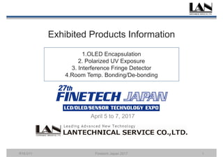
- 1. 1.OLED Encapsulation 2. Polarized UV Exposure 3. Interference Fringe Detector 4.Room Temp. Bonding/De-bonding April 5 to 7, 2017 1Finetech Japan 2017R16-011 Exhibited Products Information
- 2. 1-1.封止・貼り合わせ/Encapsulation R16-011 2 ランテクニカルサービスは様々な種類の貼り合わせ装置・封止装置を製造、販売しています。 搬送や環境管理、周辺機器とのインテグレーションも含め、封止工程をトータルでご提供します。 Lantechnical is providing the various kinds of Encapsulation, Lamination and Vacuum Assembly tools. We provide the encapsulation process totally including the environment control and the integration with other tools. Basic Spec. Substrate size G2.5 to G6.0H Vacuum 1Pa Alignment +/-1μm Finetech Japan 2017
- 3. 1-2.実験用貼り合わせ/R&D Encapsulation R16-011 3 Basic Spec. Substrate size ~ 200x200mm Vacuum 1Pa H2O, O2 Below 1 ppm ランテクニカルサービスは様々な種類の実験用・開発用貼り合わせ装置を製造、販売しています。 窒素環境管理、ディスペンサー機器とのインテグレーションも含め、貼り合わせ程をトータルでご提供します。 Lantechnical is providing the various kinds of Encapsulation tools. We provide the encapsulation process totally including the N2 Gas environment control, Dispenser and the integration with other tools. Finetech Japan 2017
- 4. 2.偏光露光装置/Polarized UV Exposure Tool R16-011 4 偏光角(Brewster’s angle)による紫外 線露光を使用し、大画面でも一括露光 が可能です。 One-shot exposure is possible to use Brewster’s angle UV exposure. 主波長 (Wave Length) 313 nm 平行度 (Parallelism) +/- 1.5 °[ 2.0 kW ] +/- 0.5 °[ 5.0 kW ] 消光比 (Extinction Ratio) 100:1 [ Center ] 照度分布 (Intensity Uniformity) +/- 3 % 照度 (Intensity) 8 mW/cm2 [ 200x200 mm ] 6 mW/cm2 [ 400x400 mm ] リニア型偏光露光装置開発中 Linear type polarized UV exposure tool is under development. Finetech Japan 2017
- 5. R16-011 5 3.干渉縞検査光源/Interference Fringe Detector セルギャップの目視検査に/Cell Gap Inspection 薄膜の目視検査に/Thin Film Inspection 干渉縞検査用の光源として/Light Source for Interference Fringe detector Basic Specification モデル(Model.) LANAX-2 主波長(Main Wage length) 589nm 発光エリア(Light Emitting area) 500x600mm ユーティリティー(Utility) 200~240V, 50 or 60Hz LANAX-2 各種サイズ対応いたします。ご相談ください。 Various sizes are ok, please contact us! Finetech Japan 2017
- 6. R16-011 Finetech Japan 2017 6 4.Room Temperature Bonding /De-bonding
- 7. What is Room Temp. Bonding?4-1. Finetech Japan 2017 Surface activation Contact Bonding Under Vacuum Condition Ar Surface oxide Contamination Room Temp. Bonding Fundamentals of Room Temp. Bonding Surface Activation – physical treatment & dry process Surface activation Ar Ion (atom) beam irradiation R16-011 7
- 8. Rapid Bonding – complete to bond within few seconds theoretically High alignment accuracy – no shift after bonding No heat effect – under room temperature process Metal, Glass, Film --- any kinds of material can be bonded Possible to control the peel strength --- Not only Bonding process but also De-Bonding process can be available. Finetech Japan 2017 4-2. Features of Room Temp. Bonding R16-011 8
- 9. In 2012, Lantechnical Service has developed "Room temperature bonding with using Si Interlayer" which is improved from the conventional Room Temperature bonding technology, with Suga Laboratory from the University of Tokyo. This technology makes possible to bond Glass and Glass, Glass and Polymer, Polymer and Polymer. Room Temp. Bonding with Si Interlayer Finetech Japan 2017 4-3. R16-011 9
- 10. What is the difference? Conventional vs. Si Interlayer Finetech Japan 2017 4-4. R16-011 10 Material A Material A Material B Feature of Lantechʼs Room Temp. Bonding is to use Si Interlayer. We use Si Interlayer for the bonded interface. This is our original method, and this is very unique technology. ConventionalConventional Si InterlayerSi Interlayer Si Interlayer Material A Bonded Interface
- 11. Metallic bond Covalent bond Ionic Bond Polymer Film Soft Metals Al, Cu Au, Su Hard Metals Ti, Ta, Fe Semiconductors Si, Ge, C, GaAs, GaP, GaN, InP NitrideSiN, TiN Carbide, Oxide SiC Al2O3, SiO2, LiNbO, LiTaO, Superconductors YBaCUo PI, PET, PEN, etc. Conventional VS Si Interlayer Conve ntional Si Inter layer Conve ntional Si Inter layer Conve ntional Si Inter layer Conve ntional Si Inter layer Conve ntional Si Inter layer Conve ntional Si Inter layer Soft Metals Al, Cu Au, Su ○ ○ ○ ○ ○ ○ ○ ○ ○ ○ N/A ○ Hard Metals Ti, Ta, Fe △ ○ △ ○ △ ○ △ ○ N/A ○ Semico nductor s, etc ○ ○ ○ ○ △ ○ N/A ○ Nitride SiN, TiN △ ○ △ ○ N/A ○ Carbide, Oxide SiC Al2O3, etc × ○ N/A ○ PI, PET, PEN, etc. N/A ○ MetallicbondCovalentbondIonic bond Polymer Film Bendability (Conventional Room Temperature Bonding vs. Si Interlayer bonding) 4-5. Finetech Japan 2017 11R16-011
- 12. What Room Temp. Bond can do? Finetech Japan 2017 4-6. Adhesives are not allowed. Applying Heat is not allowed Bond dissimilar materials Bond for De-Bond We can bond the materials with Room Temperature Bonding technology with Si Interlayer which is improved from the conventional Room Temp. bonding technology. Example, 常温接合が解決できます [Bondable] --- Glass and Glass, Glass and Film, Film and Film, Film and Metals --- Possible to bond Dissimilar materials. [Features of bonding] No Heat, No Adhesives. Intermolecular bonding. [Control of Peel strength] Not only strong bonding but also de-bonding if necessary. The peel strength can be controlled with Room Temp. Bonding Features; Solved by Room Temp. Bonding R16-011 12
- 13. Conditions of Room Temp. Bonding Finetech Japan 2017 4-7. Surface Roughness R-Max 10 nm below Room Temp. Bonding is Direct Contact Bonding technology by Intermolecular bonding. They can be bonded by low pressure contact if the surface roughness is below R-Max 10nm. The rough surface material such as Metal, we can provide the solution of bonding based on the roughness of the materials. Pressing (few ton N/cm2) < Roughness vs. Bonding Method > Possible to Bond* Surface Roughness R-Max 10 nm over Surface Roughness R-Max 10 nm over Surface Polish (CMP) ★We propose the best bonding solution according to the surface state of the customer's material. Low Pressure Contact *depends on the material properties R16-011 13
- 14. De-BOND R16-011 Finetech Japan 2017 14 Applications of Room Temperature Bonding are very diverse. There are two major fields, one is for Bonding and another is for De-bonding. Each field has several applications. OLED Lighting MEMS Packaging Battery Packaging LCD Panel Alternative to HF etching Flexible Device Transfer Si Wafer Back Grind process 4-8. Applications of Room Temp. Bonding OLED Display BOND GOG process (Glass on Glass)
- 15. Encapsulation of OLED display Finetech Japan 2017 Application of the Encapsulation process of OLED Display 4-9. • OLED display is attracting attention as the next generation display, especially expected as a flexible display. • The encapsulation technology is an important process technology for OLED display because OLED should be protected from the penetration of the moisture and oxygen. • It is possible to respond to the flexible display, and also to have the sufficient sealing performance with Room Temp. Bonding technology. OLED panel Encapsulated with Room Temp. Bonding R16-011 15 *PDL = Pixel Divided Layer Barrier film or UTG TFT GR B PI Film SiN Si PI [1~2μm] [4~8nm] [10~30nm] Passivation [Organic / Inorganic layers] Barrier film or UTG PI Film WVTR: 2×10^-2[g/m^2・day] PDL*
- 16. 剥離:常温接合 /De-Bonding:Room Temp. Bonding R16-010 16 高温プロセスに対応した after High Temperature Process 貼って剥がす De-bonding 仮止め Temporary Fix 薄物・フィルム搬送 Thin Film Transfer お困りではありませんか? 高温プロセス後でも、剥がせます! Possible to de-bond 常温接合剥離 De-bonding by Room Temp. Bonding Finetech Japan 2017 4-10.
- 17. Finetech Japan 2017 Thin glass/UTG Glass Bonding Customer’s Process De-Bonding Bonding De-Bonding Film Glass 4-11.Bond/De-bond of Thin Glass/Film with Carrier glass 1) Possible to bond Glass/Film to Glass 2) Possible to De-bond even if heated during the process. (Heating is not necessary for de-bond) Features of RTB R16-011 17 TFT process Heat process Coating process Wet process etc…
- 18. Alternative technology instead of the process of Chemical etching of LCD panels for slimming Finetech Japan 2017 ODF C F HF Chem. Etching RTB BONDING Bonding Thin Glass + Carrier Glass De-bonding Debond LCD panel from carrier glass. Carrier Glass can be reused De-bond Glass Maker Glass Maker LCD Panel Maker T F T Polarizing Plate Module ODF C F T F T Polarizing Plate Module Current Process Proposed Process LCD Panel Maker (e.g.)High temperature process/450℃@90min 4-12. We propose the new process technology, alternative to the chemical HF polishing. It is the solution of using the carrier glass to transfer the thin glass which is bonded by RTB. Cost of HF Environmental issues Limit in possible thickness Current Issues Alternative No need HF Much thinner glass Merit of Proposal Use of existing tools Low cost operation R16-011 18
- 19. Ion Beam Finetech Japan 2017 Evaluation Test4-13. Evaluation Test of Room Temp. Bonding We have an experimental tool in our factory and ready to test with Customerʼs material. Please contact the windows in the next page if you have any questions and requests. Experimental Tool in Gunma Factory R16-011 19
- 20. お問い合わせ/Contact R16-011 Finetech Japan 2017 20 Area Window E-mail Language East of Japan Hideaki Otomo otomo@lantechnical.co.jp Japanese/English West of Japan Tsutomu Ueda t-ueda@lantechnical.co.jp Japanese China/Taiwan Jack Wang jackwang@lantechnical.co.jp Chinese/Japanese Korea Choi Chulho chulho-choi@lantechkr.com Korean/Japanese Other area Hideaki Otomo otomo@lantechnical.co.jp English