ACCELEROMETER BASED GESTURE ROBO CAR
•
3 likes•4,077 views

This was my final year project based on embedded system this is the code http://downloads..com/download/24001476/code.rar.html and the pcb are http://downloads..com/download/24001498/pcb.rar.html

Recommended
More Related Content
What's hot
What's hot (20)
Similar to ACCELEROMETER BASED GESTURE ROBO CAR
Similar to ACCELEROMETER BASED GESTURE ROBO CAR (20)
Recently uploaded
Recently uploaded (20)
ACCELEROMETER BASED GESTURE ROBO CAR
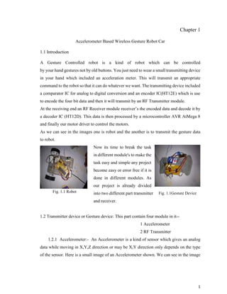
- 1. 1 Chapter 1 Accelerometer Based Wireless Gesture Robot Car 1.1 Introduction A Gesture Controlled robot is a kind of robot which can be controlled by your hand gestures not by old buttons. You just need to wear a small transmitting device in your hand which included an acceleration meter. This will transmit an appropriate command to the robot so that it can do whatever we want. The transmitting device included a comparator IC for analog to digital conversion and an encoder IC(HT12E) which is use to encode the four bit data and then it will transmit by an RF Transmitter module. At the receiving end an RF Receiver module receiver’s the encoded data and decode it by a decoder IC (HT12D). This data is then processed by a microcontroller AVR AtMega 8 and finally our motor driver to control the motors. As we can see in the images one is robot and the another is to transmit the gesture data to robot. Now its time to break the task in different module's to make the task easy and simple any project become easy or error free if it is done in different modules. As our project is already divided into two different part transmitter and receiver. 1.2 Transmitter device or Gesture device: This part contain four module in it-- 1 Accelerometer 2 RF Transmitter 1.2.1 Accelerometer:- An Accelerometer is a kind of sensor which gives an analog data while moving in X,Y,Z direction or may be X,Y direction only depends on the type of the sensor. Here is a small image of an Accelerometer shown. We can see in the image Fig. 1.1 Robot Fig. 1.1Gesture Device
- 2. 2 that there are some arrow showing if we tilt these sensor's in that direction then the data at that corresponding pin will change in the analog form. The Accelerometer having 5 pin- 1- VDD- We will give the +5volt to this pin 2- GND- We simply connect this pin to the ground for biasing. 3- X- On this pin we will receive the analog data for x direction movement. 4- Y- On this pin we will receive the analog data for y direction movement. 5- Z- On this pin we will receive the analog data for z direction movement. 6- ST- this pin is use to set the sensitivity of the accelerometer 1.5g/2g/3g/4g. 1.2.2 RF Transmitter Module (TX):- The transmitter module is working on the frequency of 433MHz and is easily available in the market at the cost of 450rs. 1- The vcc pin is connected to the +terminal in the circuit. 2- The data pin is connected to the HT12E (pin no-17) that is transmitted or we can say that encoded data. 3- The next pin is shown in figure is GND that is connected to the ground terminal. 4- Now the last pin ANT this is connected to a small wire as an antenna. 1.2.3 Processor (microcontroller): The processing is the most important part of the robot. Till now we get the data from the decoder now based on that data we have to make some decision so here the role of microcontroller is coming up. We use an Atmel atmega 8 microcontroller for our circuit to give them a decision capability. The basic circuit to initialize the microcontroller is shown below. We just need a reset circuit and oscillator to run the program. 1.3 Receiver or Robot: This part contain four module-- 1. Receiver 2. Process(microcontroller Atmel Atmega8) 3. Actuator (Motor driver L293) Fig. 1.3 Accelerometer
- 3. 3 1.3.1 RF Receiver Module (RX):- The RF receiver module will receive the data which is transferred by the gesture device. It is also working as similar to the transmitter module. 1- Connect the +vcc pin to the 5volt terminal 2- Connect the ground pin to the ground terminal 3- The data pin is then connected to the microcontroller 1.3.2 Process (Microcontroller At mega 8) :The processing is the most important part of the robot. Till now we get the data from the decoder now based on that data we have to make some decision so here the role of microcontroller is coming up. We use an 8051 microcontroller for our circuit to give them a decision capability. 1.3.3 Actuator's: The Actuator's are those devices which actually gives the movement or to do a task like motor's. In the real world there are various types of motors available which works on different voltages. So we need motor driver for running them through the controller. To get interface between motor and microcontroller. We use L293D motor driver IC in our circuit. Fig. 1.4 RF Transmitter
- 4. 4 Chapter 2 Atmega 8 2.1 History: AVR was developed in the year 1996 by Atmel Corporation. The architecture of AVR was developed by Alf-Egil Bogen and Vegard Wollan. AVR derives its name from its developers and stands for Alf-Egil Bogen Vegard Wollan RISC microcontroller, also known as Advanced Virtual RISC. The AT90S8515 was the first microcontroller which was based on AVR architecture however the first microcontroller to hit the commercial market was AT90S 1200 in the year 1997. AVR microcontrollers are available in three categories: 1. Tiny AVR 2. Mega AVR 3. Xmega AVR 2.2 Features of Atmega8 1. High-performance, Low-power Atmel AVR 8-bit Microcontroller 2. Advanced RISC Architecture 3. High Endurance Non-volatile Memory segments 4. Peripheral Features 5. Special Microcontroller Features 6. I/O and Packages 7. Operating Voltages 8. Speed Grades 9. Power Consumption at 4Mhz, 3V, 25 °C The ATmega8 provides the following features: 8 Kbytes of In-System Programmable Flash with Read-While-Write capabilities, 512 bytes of EEPROM, 1 Kbyte of SRAM, 23 general purpose I/O lines, 32 general purpose working registers, three flexible Timer/Counters Fig 2.1 AVR Microcontroller
- 5. 5 with compare modes, internal and external interrupts, a serial programmable USART, a byte oriented Two-wire Serial Interface, a 6-channel ADC (eight channels in TQFP and QFN/MLF packages) with 10-bit accuracy, a programmable Watchdog Timer with Internal Oscillator, an SPI serial port, and five software selectable power saving modes. The Idle mode stops the CPU while allowing the SRAM, Timer/Counters, SPI port, and interrupt system to continue functioning. The Power-down mode saves the register contents but freezes the Oscillator, disabling all other chip functions until the next Interrupt or Hardware Reset. In Power-save mode, the asynchronous timer continues to run, allowing the user to maintain a timer base while the rest of the device is sleeping. The ADC Noise Reduction mode stops the CPU and all I/O modules except asynchronous timer and ADC, to minimize switching noise during ADC conversions. In Standby mode, the crystal/resonator Oscillator is running while the rest of the device is sleeping. This allows very fast start-up combined with low-power consumption. The device is manufactured using Atmel’s high density non-volatile memory technology. The Flash Program memory can be reprogrammed In-System through an SPI serial interface, by a conventional non-volatile memory programmer, or by an On-chip boot program running on the AVR core. The boot program can use any interface to download the application program in the Application Flash memory.
- 6. 6 2.2 Pin Configuration Fig 2.2 At mega 8 Pin Configuration
- 7. 7 Chapter 3 Interfacing to ATmega8 I/O Ports 3.1 Introduction: ATmega8 has 32 I/O pins to communicate with external devices. Before interfacing with external devices, these pins must be configured as input or output pin .All the four ports can be configured to read an input from some external device or to give output to any external device as per the application .A single port can be configured such that some of the pins of the same port are input and some are output. 3.2 Configuring I/O Ports: Every port (PORTx, x = A or B or C or D) of AVR microcontrollers have three registers associated with it: 1. DDRx: Data direction Register, to set the direction of each pin of PORTx and configuring it to be as input or output. 2. PORTx: The values which are to be supplied at the output of the port are written in this register. These values acts as input to the device connected at output port of the microcontroller (through PORTx output configured pins). 3. PINx: This register stores the input value from the external connected hardware, when the port is configured as input port. The input data is read from PINx register. 3.3 Switch on I/O Ports: It is always best connecting the switch to ground with a pull-up resistor. When the switch is open, the 10k resistor supplies very small current needed for logic 1. When it is closed, the port pin is short to ground. The voltage is 0V and the entire sinking current requirement is met, so it is logic 0. The 10k resistor will pass 0.5 mA (5 volt/10k ohm). Thus the circuits waste very little current in either state. Fig 3.1 Switch Connection
- 8. 8 3.4 LED on I/O Ports: The resistor limits the current. The resistance can be calculated by assuming its voltage is above 2.5V and the C output is 0.9V. For 2.2V LED, 1 .9V is across the resistor so the 220 ohm would limit the current to 8.6mA (1.9/220). For 1.7V LED, 2.4V is across the resistor so it would limit the current to 10.9mA (2.4/220). The resistor should not less than 100 ohm or the LED would fail. Fig3.2 LED Connection
- 9. 9 Chapter 4 AVR Timer 4.1 Introduction The timer systems on the AVR series of Microcontroller are complex beasts. They have a myriad of uses ranging from simple delay intervals right up to complex PWM generation. We use timers every day – the simplest can be found on wrist. A simple clock will time the seconds, minutes and hours elapsed in a given day. AVR timer do a similar job, measuring a given time interval. So basically, a timer is a register, but not a normal one. The value of this register increases/decreases automatically. In AVR, timers are of two types: 8-bit and 16-bit timers. In an 8-bit timer, the register used is 8-bit wide whereas in 16-bit timer, the register width is of 16 bits. This means that the 8-bit timer is capable of counting 2^8=256 steps from 0 to 255 as demonstrated below. The AVR timers are very useful as they can run asynchronous to the main AVR core. This is fancy way of saying that the timers are separate circuits on the AVR chip which can run independent of the main program, interacting via the control and count registers, and the timer interrupts. Timers can be configured to produce output directly to pre-determined pins, reducing the processing load on the AVR core. Fig. 4.1 Timer
- 10. 10 4.2 Basic Concept The AVR has three timers: 1. Timer 0 – 8 bit. 2. Timer 1 – 16 bit. 3. Timer 2 – 8 bit. 4.3 TCNT0 Register: The Timer/Counter Register – TCNT0 is as follows: This is where the 8-bit counter of the timer resides. The value of the counter is stored here and increases/decreases automatically. Data can be both read/written from this register. Now we know where the counter value lies. But this register won’t be activated unless we activate the timer! Thus we need to set the timer up. The Timer/Counter Control Register – TCCR0 is as follows: Fig. 4.2 Timer Concept Fig. 4.3 Timer Register Fig. 4.4 Timer Register TCCR0
- 11. 11 We will concentrate on the highlighted bits. The other bits will be discussed as and when necessary. By selecting these three Clock Select Bits, CS02:00, we set the timer up by choosing proper prescaler. The possible combinations are shown below. 4.4 Timers Running at F_cpu Let’s say, we need to flash an LED every 6ms and we are have a CPU clock frequency of 32 kHz. We initialize the counter as: TCCR0 |= (1 << CS00); 4.5 Code Code: #include <avr/io.h> void timer0_init() { TCCR0 |= (1 << CS00); // set up timer with no prescaling TCNT0 = 0; // initialize counter } int main(void) { Fig. 4.5 Clock Bit Set
- 12. 12 DDRC |= (1 << 0); // connect led to pin PC0 timer0_init(); // initialize timer while(1) { if (TCNT0 >= 191) // check if the timer count reaches 191 { PORTC ^= (1 << 0); // toggles the led TCNT0 = 0; // reset counter } } }
- 13. 13 Chapter 5 AVR USART 5.1 Introduction The Universal Synchronous and Asynchronous serial Receiver and Transmitter (USART) is a highly flexible serial communication device. The USART hardware allows the AVR to transmit and receive data serially to and from other devices such as a computer or another AVR. 5.2 Main features are: 1. Full Duplex Operation (Independent Serial Receive and Transmit Registers) 2. Asynchronous or Synchronous Operation 3. Master or Slave Clocked Synchronous Operation 4. High Resolution Baud Rate Generator 5. Supports Serial Frames with 5, 6, 7, 8, or 9 Data Bits and 1 or 2 Stop Bits 6. Odd or Even Parity Generation and Parity Check Supported by Hardware 7. Data Over Run Detection 8. Framing Error Detection 9. Noise Filtering Includes False Start Bit Detection and Digital Low Pass Filter 10. Three Separate Interrupts on TX Complete, TX Data Register Empty, and RX Complete 11. Multi-processor Communication Mode 12. Double Speed Asynchronous Communication Mode Atmega8 USART provides asynchronous mode of communication and do not have a dedicated clock line between the transmitting and receiving end. The synchronization is achieved by properly setting the baud rate, start and stop bits in a transmission sequence. Start bit and stop bit:
- 14. 14 These bits are used to synchronize the data frame. Start bit is one single low bit and is always given at the starting of the frame, indicating the next bits are data bits. Stop bit can be one or two high bits at the end of frame, indicating the completion of frame. 5.3 Baud Rate: In simple words baud rate is the rate at which serial data is being transferred. Baud rate of two devices must match or else they will not be able to synchronize with each other. To set Baud rate: #define USART_BAUDRATE 9600 5.4 USART Registers To use the USART of Atmega16, certain registers need to be configured. USART control and status register. It’s is basically divided into three parts UCSRA, UCSRB and UCSRC. These registers are basically used to configure the USART. USART Baud Rate Registers. Basically use to set the baud rate of USART. UDR: USART data register Initializing the USART: To initialize the USART: 1. Turn on transmission and reception circuitry. 2. Select the number of stop bits. 3. Set the size of data. 4. Load the value of UBRR to set the baud rate. Code: void usart_init() { UCSRB|=(1<<RXEN)|(1<<TXEN); // Turn on transmission and reception circuitry UCSRC|=(1<<URSEL)|(1<<UCSZ0)|(1<<UCSZ1); // use 8-bit character sizes
- 15. 15 UBRRH = (BAUD_PRESCALE>>8); UBRRL = BAUD_PRESCALE; // baud rate value into the high byte of the UBBR register } 5.5 Sending Data We can do this by checking the USART Data Register Empty flag (UDRE), also located in the UCSRA control register of ATmega8. Code: while((UCSRA & (1 << UDRE))==0) { }; // Do nothing until UDR is ready UDR = ByteToSend; // Send out the byte value in the variable” ByteToSend” 5.6 Receiving Data To do this, we can check the USART Receive Complete (RXC) flag to see if it is set. RXC is located in the UCSRA control register of ATmega8. Code: while((UCSRA & (1 << RXC))==0) { }; // Do nothing until data have been received and is ready to be read from UDR ReceivedByte = UDR; // Fetch the received byte value in the variable” ReceivedByte”
- 16. 16 Chapter 6 Accelerometer 6.1 Introduction The ADXL330 is a small, thin, low power, complete 3-axis accelerometer with signal conditioned voltage outputs, all on a single monolithic IC. The product measures acceleration with a minimum full-scale range of ±3 g. It can measure the static acceleration of gravity in tilt-sensing applications, as well as dynamic acceleration resulting from motion, shock, or vibration. The user selects the bandwidth of the accelerometer using the CX, CY, and C Z capacitors at the X OUT, YOUT, and Z OUT pins. Bandwidths can be selected to suit the application, with a range of 0.5 Hz to 1600 Hz for X and Y axes, and a range of 0.5 Hz to 550 Hz for the Z axis. The ADXL330 is available in a small, low profile, 4 mm × 4 mm × 1.45 mm, 16-lead, plastic lead frame chip scale package (LFCSP_LQ). 6.2 Theory Of Operation The ADXL330 is a complete 3-axis acceleration measurement system on a single monolithic IC. The ADXL330 has a measure-ment range of ±3 g minimum. It contains a polysilicon surface micromachined sensor and signal conditioning circuitry to implement an open-loop acceleration measurement architecture.The output signals are analog voltages that are proportional to acceleration. The accelerometer can measure the static accelera- tion of gravity in tilt sensing applications as well as dynamic acceleration resulting from motion, shock, or vibration. The sensor is a polysilicon surface micromachined structure built on top of a silicon wafer. Polysilicon springs suspend the structure over the surface of the wafer and provide a resistance against acceleration forces. Deflection of the structure is meas-ured using a differential capacitor that consists of independent fixed plates and plates attached to the moving mass. The fixed plates are driven by 180° out-of-phase square waves. Acceleration deflects the moving mass and unbalances the differential capacitor
- 17. 17 resulting in a sensor output whose amplitude is proportional to acceleration. Phase- sensitive demodulation techniques are then used to determine the magnitude and direction of the acceleration. The demodulator output is amplified and brought off-chip through a 32 kΩ resistor. The user then sets the signal band-width of the device by adding a capacitor. This filtering improves measurement resolution and helps prevent aliasing. 6.2.1 Mechanical Sensor The ADXL330 uses a single structure for sensing the X, Y, and Z axes.As a result, the three axes sense directions are highly orthogonal with little cross axis sensitivity. Mechanical mis-alignment of the sensor die to the package is the chief source of cross axis sensitivity. Mechanical misalignment can, of course, be calibrated out at the system level. 6.2.2 Performance Rather than using additional temperature compensation circuitry, innovative design techniques ensure high performance is built-in to the ADXL330. As a result, there is neither quantization error nor nonmonotonic behavior, and temperature hysteresis is very low (typically less than 3 m g over the −25°C to +70°C temperature range). This is typically better than ±1% over the −25°C to +70°C temperature range. 6.3 Functional Block Diagram Fig. 6.1 Functional Block Diagram
- 18. 18 6.4 Features 1. 3-axis sensing 2. Small, low-profile package 3. 4 mm × 4 mm × 1.45 mm LFCSP 4. Low power 5. 180 μA at V S = 1.8 V (typical) 6. Single-supply operation 7. 1.8 V to 3.6 V 8. 10,000 g shock survival 9. Excellent temperature stability 10. BW adjustment with a single capacitor per axis 11. RoHS/WEEE lead-free compliant 6.5 Applications 1. Cost-sensitive, low power, motion- and tilt-sensing applications 2. Mobile devices 3. Gaming systems 4. Disk drive protection 5. Image stabilization 6. Sports and health devices
- 19. 19 Chapter 7 Radio Transmitter & Receiver Modules 7.1 Introduction 1. The MO-SAWR is an ASK transmitter module . 2. The result is excellent performance in a simple-to-use . 3. The MO-SAWR is designed specifically for remote-control , wireless mouse and car alarm system operating at 433.92 in the USA under FCC Part 15 regulation. 7.2 Features 1. Miniature sil package 2. 3. Fully shielded 4. Data rates up to 128kbits/s 5. Range up to 300 meters 6. Single supply voltage 7. Industry pin compatible 7.3 Application 1. Car security system 2. Remote key less entry 3. Garage door controller 4. Home security 5. Wireless mouse 6. Automation system 7.4 Operation Warning 1. Do not expose the boards to direct outdoor environment. If they will be used outdoors, keep them away from water, moisture and direct sunlight. 2. The serial input and output pins operate at +5V and 0V logic levels. Do not attempt to connect directly to a computer RS232 port as this will damage the module. Typical levels at a computer RS232 port are +10V and -10V; these voltages would Fig. 7.1 RF Transmitter Fig.7.2. RF Receiver
- 20. 20 immediately damage the module. The module is intended to interface directly with the Basic Stamp 2, the BASIC Stamp 2sx and other +5V logic devices. 3. Keep the top part of the board (PCB Trace Antenna, opposite end of the 17 pin header) at least 4 inches away from any object, especially metal, wires and batteries as this will de-tune the antenna, drastically reducing performance. Laying the module flat on a work desk made of wood, plastic or glass can sometimes cause problems as well, since some paints contain conductive materials. 4. Do not touch the adjustable capacitor located at the top of the board. This part is factory tuned and must not be adjusted. It is set at an optimal operating position and if moved will drastically reduce performance. 5. If mounting the board, use the mounting holes located in the center and corner of the boards. Only use plastic stand-offs and plastic screws. Using any electrically conductive materials near the board will reduce performance of the board. Table 7. 1Operating Parameters
- 21. 21 Chapter 8 Software Tool 8.1 Eclipse Juno Eclipse is a community for individuals and organizations who wish to collaborate on commercially- friendly open source software. Its projects are focused on building an open development platform comprised of extensible frameworks, tools and runtimes for building, deploying and managing software across the lifecycle. The ECLIPES Foundation is a not-for-profit, member supported corporation that hosts the ECLIPES PROJECT and helps cultivate both an open source community and an ecosystem of complementary products and services. 8.1.1 History of Eclipse Industry leaders Borland, IBM, MERANT, QNX Software Systems, Rational Software, Red Hat, SuSE, TogetherSoft and Webgain formed the initial eclipse.org Board of Stewards in November 2001. By the end of 2003, this initial consortium had grown to over 80 members. On Feb 2, 2004 the Eclipse Board of Stewards announced Eclipse’s reorganization into a not-for-profit corporation. Originally a consortium that formed when IBM released the Eclipse Platform into Open Source, Eclipse became an independent body that will drive the platform’s evolution to benefit the providers of software development offerings and end-users. All technology and source code provided to and developed by this fast-growing community is made available royalty-free via the Eclipse Public License. The founding Strategic Developers and Strategic Consumers were Ericsson, HP, IBM, Intel, MontaVista Software, QNX, SAP and Serena Software. 8.1.2 Application Development Fig. 8.1 Eclipse Divergence
- 22. 22 8.2 Dip Trace : DipTrace is EDA software for creating schematic diagrams and printed circuit boards. The first version of DipTrace was released in August, 2004. The latest version as of March 2013 is DipTrace version 2.3.1. The interface and tutorials are multi-lingual (currently English, Czech, Russian and Turkish) In January of 2011Parallax switched from Eagle to DipTrace for developing its printed circuit boards. 8.2.1 Modules: 1. Schematic Design Editor 2. PCB Layout Editor 3. Component Editor 4. Pattern Editor 5. Shape-Based AutoRoute 6. 3D PCB Preview Fig. 8.2 AVR Installation
- 23. 23 8.2.2 Smart Project Structure Dip Trace is single environment with direct circuit-to-board conversion, updating from schematic and back annotation. Nets are divided to net classes with custom settings and class-to-class rules. Through and blind/buried visa are organized to Via Styles. 8.2.3 Placement Features Components can be placed manually by simple drag and drop and special "Place by list" feature or automatically according to custom settings and with optimized length of traces. For excellent results use combination of all available placement methods. Fig. 8.3 Dip Trace Product Fig. 8.4 Placement Feature
- 24. 24 8.2.4 High-Speed AutoRoute Dip Trace high-class shape-based auto router with advanced settings is capable of routing complex multi-layer boards, as well as simple single-layer boards with jumper wires. DSN/SES interface provides support for external routers (Spectra, Electra, Toper etc.) 8.2.5 Manual Routing Traces can be created with 15, 30, 45, 90-degree and free angle lines or with arcs and curves. Hot keys allow to change route mode, current segment's geometry, width, layer, via style and other parameters on the go. Existing traces can be easily moved or changed without losing geometry, while different highlight options ensure friendly working process. Smart shape-based copper pour system with pour priority and automated settings expand engineering opportunities even more. 8.2.6 Advanced Verification Features Fig. 8.5 Routing Variation Fig. 8.6 More DipTrace Option
- 25. 25 Dip Trace provides error-free design environment, from component creation to board manufacturing. DRC verifies clearances between design objects and size limits, while rules are defined by object types, layers, net classes and class-to-class settings. Real-time DRC checks every action and shows errors before actually making them. Net Connectivity guarantees, that all nets had been properly routed and reports broken and merged nets. Comparing to schematic allow to find differences between PCB and source schematic.
- 26. 26 Chapter 9 PCB Layouts 9.1 Receiver Bot Fig.9.1 Receiver Bot Top View Fig.9.2 Receiver Bot Bottom View
- 27. 27 9.2 Transmitter Bot Fig.9.3 Transmitter Bot Top View Fig.9.4 Transmitter Bot Bottom View
- 28. 28 9.3 Motor Driver Fig.9.5 Motor Drive Top View Fig.9.6 Motor Drive Bottom View
- 29. 29 9.4 Supply Filter Fig.97 Supply Filter Top View Fig.9.8 Supply Filter Bottom View
- 30. 30 Chapter 10 Conclusion As we all know, these days India is sick off massive terror attacks and bomb explosions. To avoid such disasters technological power must exceed human power. Human life and time are priceless. So in this project, we propose a model of a robot based on “Human Machine Interfacing Device” utilizing hand gestures to communicate with embedded systems for tracking of enemies. The 3-axis accelerometer is selected to be the input device of this system, capturing the human arms behaviors. When compared with other common input devices, especially the teach pendant, this approach using, accelerometer is more intuitive and easy to work, besides offering the possibility to control a robot by wireless means. Using this system, a non-expert robot programmer can also control a robot quickly and in a natural way. In further advancement this project can be taken to the next level by using the wireless camera that can capture images. With the installation on camera with this system can make this project a military useful project. For commercial purpose this project may be helpful to the paralyses patients who cant walk but can move hand. The mechanism used in project i.e. controlling as gesture be used in the wheel chairs for them.
- 31. 31 References [1] S. Waldherr, R. Romero, and S. Thrun, “A gesture based interface for human- robot interaction,” in Autonomous Robots, vol. 9, o.2, pp. 151-173, Springer, 2000. [2] I. Mihara, Y. Yamauchi, and M. Doi, “A real-time vision-based interface using motion processor and applications to robotics,” in Systems and Computers in Japan, vol. 34, pp. 10-19, 2003. [3] S. Perrin, A. Cassinelli, and M. Ishikawa, “Gesture recognition using laser-based tracking system,” in Sixth IEEE International Conference on Automatic Face and Gesture Recognition, pp. 541-546, 2004. [4] Martin Urban, Peter Bajcsy, Rob Kooper and Jean-Chistophe “Recognition of Arm Gestures Using Multiple orientation sensors,” Lementec2004 IEEE Intelligent Transportation Systems conference Washington, D.C., USA, October34,2004. [5] Tan Tian Swee, A.K. Ariff, Sh-Hussain.Salleh, Siew Kean Seng and Leong Seng Huat “Data Gloves Malay Sign Language Recognition System” 1-4244-0983- 7/07/$25.00 ©2007 IEEE. [6] Robert Lemoyne, Christian Coroian, and Timothy Mastroianni “Wireless accelerometer system for quantifying gait,” 978-1-4244-3316-2/09/$25.00©2009IEEE. [7] Pedro Neto, J. Norberto Pires, and A. Paulo Moreira, “Accelerometer-Based Control of an Industrial Robotic Arm”, IEEE International Symposium on Robot and Human Interactive Communication, Toyama, Japan, 2009.