
Recomendados
Recomendados
Mais conteúdo relacionado
Mais procurados
Mais procurados (20)
Semelhante a MIP6S10MTSCF Product Standards
Semelhante a MIP6S10MTSCF Product Standards (20)
Mais de AUTHELECTRONIC
Mais de AUTHELECTRONIC (20)
Último
Último (20)
MIP6S10MTSCF Product Standards
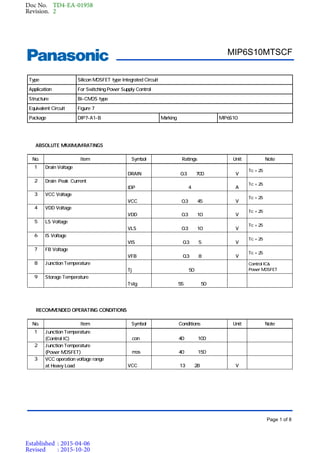
- 1. Page 1 of 8 Product Standards MIP6S10MTSCF Type Silicon MOSFET type Integrated Circuit Application For Switching Power Supply Control Structure Bi-CMOS type Equivalent Circuit Figure 7 Package DIP7-A1-B Marking MIP6S10 A.ABSOLUTE MAXIMUM RATINGS No. Item Symbol Ratings Unit Note 1 Drain Voltage Tc = 25℃ DRAIN −0.3 ∼ 700 V 2 Drain Peak Current Tc = 25℃ IDP 4 A 3 VCC Voltage Tc = 25℃ VCC −0.3 ∼ 45 V 4 VDD Voltage Tc = 25℃ VDD −0.3 ∼ 10 V 5 LS Voltage Tc = 25℃ VLS −0.3 ∼ 10 V 6 IS Voltage Tc = 25℃ VIS −0.3 ∼ 5 V 7 FB Voltage Tc = 25℃ VFB −0.3 ∼ 8 V 8 Junction Temperature Control IC& Power MOSFETTj 150 ℃ 9 Storage Temperature Tstg −55 ∼ +150 ℃ B.RECOMMENDED OPERATING CONDITIONS No. Item Symbol Conditions Unit Note 1 Junction Temperature (Control IC) Tjcon −40 ∼ +100 ℃ 2 Junction Temperature (Power MOSFET) Tjmos −40 ∼ +150 ℃ 3 VCC operation voltage range at Heavy Load VCC 13 ∼ 28 V Doc No. TD4-EA-01958 Revision. 2 Established : 2015-04-06 Revised : 2015-10-20
- 2. Page 2 of 8 Product Standards MIP6S10MTSCF C.ELECTRICAL CHARACTERISTICS Measurement conditions (Ta=25℃±3℃) NO. Item Symbol Measurement Conditions Typ. Min. Max. Unit 【CONTROL FUNCTIONS】 *Design Guarantee Item, **Reference Item 1 VCC Start Voltage VCC(ON) 18.5 17.0 20.0 V 2 VCC Stop Voltage VCC(OFF) 10.8 9.8 11.8 V 3 VCC Start/Stop Hysteresis VCC(ON) - VCC(OFF) D_VCC 7.7 6.9 8.8 V 4 VDD Reference Voltage VCC = 21 V VDD 5.9 5.6 6.2 V 5 Circuit Current before start VCC = VCC(ON) - 0.8 V, FB : openICC(SB) 0.58 0.48 0.68 mA 6 Operating Circuit Current at light load VCC = 15 V, IFB = IFB1 ‒ 10 μAICC(STB) 0.51 0.45 0.56 mA **7 Operating Circuit Current VCC = 21 V, IFB = -20 μA, DRAIN = 5 V mAICC(OP) 1.50 - - 8 Operating Circuit Current VCC = 15 V VFB = VFB(OL) → openat Over Load Protection ICC(OL) 0.85 0.70 1.00 mA 9 Output Frequency VCC = 21 V, VFB = 3 V, DRAIN = 5 Vfosc 66 61 71 kHz 10 Jitter Frequency Deviation VCC = 21 V, VFB = 3 V, DRAIN = 5 Vd_fosc 3.0 1.8 4.2 kHz **11 Jitter Frequency Modulation Rate VCC = 21 V, VFB = 3 V, DRAIN = 5 VfM 350 - - Hz 12 Maximum Duty Cycle VCC = 21 V, VFB = 3 V, DRAIN = 5 VMAXDC 66 60 72 % 13 Feedback Threshold Current ON → OFF, VCC = 21 VIFB1 -80 -104 -56 μA **14 Feedback Current Hysteresis OFF → ON, VCC = 21 VIFBHYS 1 - - μA 15 FB Pin Voltage VCC = 21 V, IFB = IFB1 VFB1 1.6 1.4 1.8 V 16 FB Pin Grounded Current VCC = 21 V, VFB = 0 V IFB0 -330 -410 -250 μA 17 FB Pin Pull-down resistance VCC = 40 V, VFB = VFB1 at Output Stop RFB(OFF) 400 250 550 Ω Doc No. TD4-EA-01958 Revision. 2 Established : 2015-04-06 Revised : 2015-10-20
- 3. Page 3 of 8 Product Standards MIP6S10MTSCF No. Item Symbol Measure Conditions Typ. Min. Max. Unit 18 VCC Pin Charging Current VCC = 0 V, FB : open, DRAIN = 50 VICCH1 -11.0 -15.4 -6.6 mA VCC = VCC(ON) - 0.5 V, FB : open, DRAIN = 50 VICCH2 -3.0 -5.0 -2.0 mA *19 Soft Start Time DRAIN = 50 V Tsoft 6.0 3.5 8.5 ms 【CIRCUIT PROTECTIONS】 *Design Guarantee Item, **Reference Item 20 Current Limit Detection Maximum VCC = 21 V, VFB = 3 V, DRAIN = 5 VVoltage VLIMIT(MAX) 800 744 856 mV 21 Current Limit Detection Maximum VCC = 21 V, VFB = 3 V, VLS = 0.75 V, DRAIN = 5 VVoltage at Input Compensation Mode VLIMIT_L 710 660 760 mV 22 Slope Compensation Rate VCC = 21 V, VFB = 3 V VLIM_SLP -19.5 -24.0 -14.5 mV/μs *23 Start Duty Cycle of VCC = 21 V, VFB = 3 V Slope Compensation D_SLP 35.0 31.5 38.5 % *24 Current Detection Minimum Voltage VCC = 21 V, IFB = IFB1, DRAIN = 5 Vat light load VIS(OFF)min 160 110 210 mV **25 Jitter Deviation of Current Detection VCC = 21 V, IFB = IFB1, DRAIN = 5 V mVVoltage at light load D_VIS(OFF) 40 - - 26 LS Pin Voltage of VCC = 21 V, VFB = 3 V, DRAIN = 5 VInput Compensation Detect VLS(CL) 520 468 572 mV 27 LS Pin Voltage of VCC = 21 V, VFB = 3 V, DRAIN = 5 VInput Compensation Release VLS(CL)L 470 423 517 mV 28 LS Pin Hysteresis Voltage of VCC = 21 V, VFB = 3 V, DRAIN = 5 VInput Compensation VLS(CL)HYS 60 45 75 mV 29 LS Pin Voltage of VCC = 21 V, VFB = 3 V, DRAIN = 5 VOver Input Protection Detect VLS(OV) 1.050 0.945 1.155 V 30 LS Pin Voltage of VCC = 21 V, VFB = 3 V, DRAIN = 5 VOver Input Protection Return VLS(OV)L 1.000 0.900 1.100 V 31 LS Pin Hysteresis Voltage of VCC = 21 V, VFB = 3 V, DRAIN = 5 VOver Input Protection VLS(OV)HYS 0.060 0.045 0.075 V 32 VCC timer Count VCC = VCC(ON) ⇔VCC(OFF) at Over Load Protection OLP_CNT 4 - **33 Leading Edge Blanking Delay Ton(BLK) 440 - - ns **34 Current Limit Delay Td(OCL) 150 - - ns 35 FB Over Load Protection detect VCC = 22 V, DRAIN = 5 VVoltage VFB(OL) 4.4 4.1 4.7 V 36 FB Current at heavy load VCC = 22 V, VFB = 3 V, DRAIN = 5 VIFB(OL) -10 -13 -7 μA Doc No. TD4-EA-01958 Revision. 2 Established : 2015-04-06 Revised : 2015-10-20
- 4. Page 4 of 8 Product Standards MIP6S10MTSCF No. Item Symbol Measure Conditions Typ. Min. Max. Unit 37 VCC Over Voltage Protection VFB = 3 V, DRAIN = 5 VVCC(OV) 31.5 28.5 34.5 V 38 VDD Over Voltage Protection VCC = 21 V, VFB = 3 V, DRAIN = 5 VVDD(OV) 7.5 7.0 8.1 V 39 VDD current at VDD Over Voltage VCC = 21 V, VFB = 3 V, DRAIN = 5 VProtection IDD(OV) 1.2 0.7 1.7 mA 40 VDD Clamp Current VDD = 10 V IDD(CLP) 16.5 13.2 19.8 mA **41 Over Load Protection Filter Time VCC = 21 V Td(OL) 20 - - μs **42 Over Voltage Protection VCC = 21 V Latch Stop Filter Time Td(LAT) 150 - - μs 43 Latch Reset VDD Threshold Voltage VDDreset 2.7 1.7 3.7 V *44 Thermal Shutdown Temperature (Control IC) TOTP 140 130. 150 ℃ **45 Thermal Shutdown Temperature Hysteresis (Control IC) TOTPHYS 70 - - ℃ 【Power MOSFET】 *Design Guarantee Item, **Reference Item 46 Minimum Drain Supply Voltage VD(MIN) 25.0 20.0 29.0 V 47 Breakdown Voltage VCC = 40 V, IDRAIN = 250 μA,VDSS - 700 - V 48 OFF-State leakage Current VCC = 40 V DRAIN = 650 VIDSS 2 - 7 μA 49 ON-State Resistance VCC = 21 V, VFB = 3 V, IDRAIN = 1 A, ΩRDS(ON) 2.5 - 2.7 **50 Rise Time VCC = 21 V, VFB = 3 V, DRAIN = 5 V nstr 150 - - **51 Fall Time VCC = 21 V, VFB = 3 V, DRAIN = 5 V nstf 80 - - Doc No. TD4-EA-01958 Revision. 2 Established : 2015-04-06 Revised : 2015-10-20
- 5. Page 5 of 8 Product Standards MIP6S10MTSCF 【Figure 1: Measurement circuit/Pin Layout】 【Figure 2: fosc, d_fosc, fM measurement】 Pin No. Pin Name Function 1 FB Feedback control 2 GND Ground 3 LS Input Compensation / Over Input Voltage Protection 4 IS MOSFET Source / Current Detection 5 DRAIN MOSFET Drain / Power supply for start-up 6 7 VCC Power supply from bias winding / Over Voltage Protection 8 VDD Reference Voltage for circuits / External latch Protection 1 2 3 4 8 7 5 1 2 3 4 8 7 5 1 2 3 4 8 7 5 1 2 3 4 8 7 5 d_fosc time frequency fosc (average) 1/fM VFB /IFB VIS /IIS 1 2 4 6.8 kΩ 3μF VLS /ILS 1μF 3 VDD /IIDD VCC /ICC VDRAIN /IDRAIN 0.1μF L Rd 1μF 8 7 5 Rs 0.1μF Doc No. TD4-EA-01958 Revision. 2 Established : 2015-04-06 Revised : 2015-10-20
- 6. Page 6 of 8 Product Standards MIP6S10MTSCF 【Figure 3: VLS−VLIMIT Characteristics】 【Figure 4: IFB−VLIMIT Characteristics】 VLS VLIMIT VLIMIT(MAX) VLIMIT_L 0 VLS(CL) VLS(CL)HYS VLS(OV) VLS(OV)HYS (発振停止)(Oscillation stop) | IFB(OL) | VLIMIT(MAX) VIS(OFF)min Current Limit Detection threshold Voltage of IS | IFB | IFBHYS Oscillation restart Oscillation stop | IFB1 | Doc No. TD4-EA-01958 Revision. 2 Established : 2015-04-06 Revised : 2015-10-20
- 7. Page 7 of 8 Product Standards MIP6S10MTSCF 【Figure 5: Over Load Protection Characteristics】 【Figure 6: tr, tf measurement】 time 10% 90% tf tr DRAIN voltage VCC(OFF) ILIMIT VCC(ON) VFB(OL) ILIMIT Tsoft Tsoft Tsoft Tsoft t(OLP) Td(OL) VDD VCC terminal Voltage Output Power FB terminal Voltage Drain Current of Power MOSFET Oscillation Stop and Timer Intermittent Oscillation Start Max Output Power Over Load Detection Oscillation stop Oscillation restart Max Output Power Doc No. TD4-EA-01958 Revision. 2 Established : 2015-04-06 Revised : 2015-10-20
- 8. Page 8 of 8 Product Standards MIP6S10MTSCF 【Figure 7: Block Diagram】 【Precautions for Use 1】 Connect a ceramic capacitor with value ≧ 0.1 μF between VDD pin and GND 【Precautions for Use 2】 The product has risks for break-down or burst or giving off smoke in following conditions. Avoid the following use. Fuse should be added at the input side or connect Zener diode between control pin and GND, etc. as a countermeasure to pass regulatory Safety Standard. Concrete countermeasure could be provided individually. However, customer should make the final judgment. (1) Reverse the Drain pin and FB pin connection to the power supply board. (2) Connect to pins in which different Maximum ratings. VDD FB VCC(ON)/ VCC(OFF) + - VDD External Latch + - VFB(OL) Clamping Circuit I-V Converter Oscillator with Jitter + -VIS(OFF) Light load Detection Over Temp. Detection MAXDUTY CLOCK Under Voltage Lock Out Restart Trigger Regulator + - Vdrv = 12.5V VCC + - + - VCC(OV) DRAIN GND Power MOSFET S QR Q Timer Intermittent IS LS VLIMIT(MAX) VLIMIT_L Lower Limit with Jitter + - Slope Compensation Over Input voltage Detection VLIMIT Change Lower Limit with Jitter + - + - Slope Compensation Over Input voltage Detection VLIMIT Change RC filter S QR Q Leading Edge Blanking Doc No. TD4-EA-01958 Revision. 2 Established : 2015-04-06 Revised : 2015-10-20
- 9. Request for your special attention and precautions in using the technical information and semiconductors described in this book (1) If any of the products or technical information described in this book is to be exported or provided to non-residents, the laws and regulations of the exporting country, especially, those with regard to security export control, must be observed. (2) The technical information described in this book is intended only to show the main characteristics and application circuit examples of the products. No license is granted in and to any intellectual property right or other right owned by Panasonic Corporation or any other company. Therefore, no responsibility is assumed by our company as to the infringement upon any such right owned by any other company which may arise as a result of the use of technical information de-scribed in this book. (3) The products described in this book are intended to be used for general applications (such as office equipment, communications equipment, measuring instruments and household appliances), or for specific applications as expressly stated in this book. Please consult with our sales staff in advance for information on the following applications, moreover please exchange documents separately on terms of use etc.: Special applications (such as for in-vehicle equipment, airplanes, aerospace, automotive equipment, traffic signaling equipment, combustion equipment, medical equipment and safety devices) in which exceptional quality and reliability are required, or if the failure or malfunction of the products may directly jeopardize life or harm the human body. Unless exchanging documents on terms of use etc. in advance, it is to be understood that our company shall not be held responsible for any damage incurred as a result of or in connection with your using the products described in this book for any special application. (4) The products and product specifications described in this book are subject to change without notice for modification and/or improvement. At the final stage of your design, purchasing, or use of the products, therefore, ask for the most up- to-date Product Standards in advance to make sure that the latest specifications satisfy your requirements. (5) When designing your equipment, comply with the range of absolute maximum rating and the guaranteed operating conditions (operating power supply voltage and operating environment etc.). Especially, please be careful not to exceed the range of absolute maximum rating on the transient state, such as power-on, power-off and mode-switching. Other- wise, we will not be liable for any defect which may arise later in your equipment. Even when the products are used within the guaranteed values, take into the consideration of incidence of break down and failure mode, possible to occur to semiconductor products. Measures on the systems such as redundant design, arresting the spread of fire or preventing glitch are recommended in order to prevent physical injury, fire, social damages, for example, by using the products. (6) Comply with the instructions for use in order to prevent breakdown and characteristics change due to external factors (ESD, EOS, thermal stress and mechanical stress) at the time of handling, mounting or at customer's process. We do not guarantee quality for disassembled products or the product re-mounted after removing from the mounting board. When using products for which damp-proof packing is required, satisfy the conditions, such as shelf life and the elapsed time since first opening the packages. (7) When reselling products described in this book to other companies without our permission and receiving any claim of request from the resale destination, please understand that customers will bear the burden. (8) This book may be not reprinted or reproduced whether wholly or partially, without the prior written permission of our company. No.010618